
Why Via Aspect Ratio Is Critical for Reliable PCB Manufacturing
14 min
- Understanding Via Aspect Ratio and Its Role in PCB Production
- Standard Guidelines and Limits for Via Aspect Ratio
- Design Strategies to Optimize Via Aspect Ratio
- Manufacturing Challenges and Professional Solutions
- JLCPCB's Expertise in Managing Via Aspect Ratio
- Frequently Asked Questions (FAQ)
Have you ever received a PCB lot back with intermittent open circuits that do not present themselves until after reflow or thermal cycling? The underlying cause, in most instances, is the one parameter that was not given much attention: the aspect ratio of the via. It is among those figures that silently dictate the life or death of your plated through-holes in the real world, or that they will grow into time bombs lurking within your board. The via aspect ratio is a ratio between two basic physical dimensions, board thickness and drilled hole diameter, that reduces to a single figure that informs your fabricator of how hard your vias will be to plate with good reliability.
Take that ratio too high, and the electroplating chemistry is unable to deposit enough copper deep in the barrel. The consequence is thin spots, voids, and later cracks that transform a successful prototype into a failure in the field. In this paper, we are going to deconstruct the definition of exactly what aspect ratio means, how it is determined, what the industry standards would be regarding standard and HDI boards, and how you can make smarter decisions when designing at the first instance of your stackup. We shall also examine how JLCPCB is controlling this parameter in its manufacturing line so as to provide the same quality plating whether in prototypes or in volume production.
Understanding Via Aspect Ratio and Its Role in PCB Production
What the Via Aspect Ratio Means and How It Is Calculated
The via aspect ratio is defined as the ratio of the board thickness (or the depth of the via) to the diameter of the drilled hole before plating. The formula is straightforward:
Aspect Ratio = Board Thickness / Drilled Hole Diameter
The two values should be of equal units, usually millimeters. Note that the calculation is done with the mechanical drill diameter, and not the finished plated hole diameter. Once copper has been electroplated on the walls of the barrel, the final hole size reduces by approximately twice the plating thickness.
Let us work through a few examples to make this concrete:
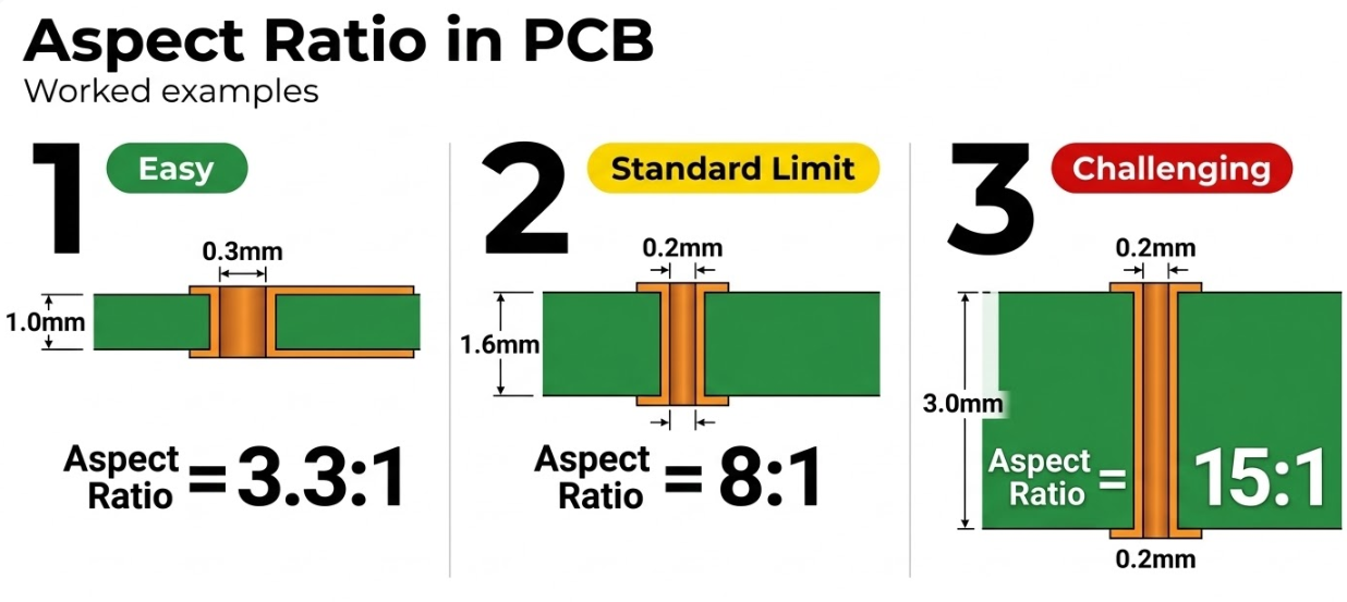
- Standard 2-layer board: A 1.6 mm thick board with a 0.3 mm drill gives an aspect ratio of 1.6 / 0.3 = 5.3:1. This is comfortable for virtually any fabricator.
- 4-layer board with smaller vias: A 1.6 mm board with a 0.2 mm drill gives 1.6 / 0.2 = 8:1. This is approaching the upper end of standard process capability and qualifies the holes as "small holes" at most fabs.
- Thick multilayer board: A 2.4 mm board (common for 8-10 layer designs) with a 0.2 mm drill gives 2.4 / 0.2 = 12:1. This exceeds the reliable plating window for most standard process lines and will require either a larger drill or advanced plating controls.
Why It Directly Affects Plating Quality and Reliability
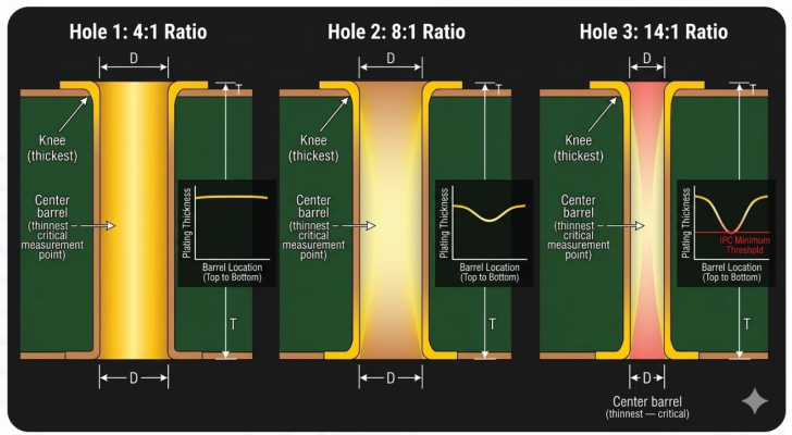
As the aspect ratio increases, two problems compound each other. First, the current density distribution becomes uneven. The electric field concentrates at the hole entrance (the "dog-bone" ends of the barrel), causing copper to deposit faster at the top and bottom than in the middle. Second, chemical transport slows down. Fresh plating solution struggles to reach the center of a deep, narrow hole, while reaction byproducts accumulate there. The deeper and narrower the hole, the worse this mass transport limitation becomes.
The practical consequences are well-documented:
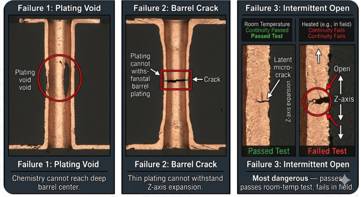
- Thin plating in the center of the barrel: The center of the barrel copper can reduce to a much lower level than the IPC-6012 minimum of 20 micrometers (Class 2) or 25 micrometers (Class 3), providing a weak point in the electrical path.
- Voids and inclusions: Voids are formed by captured air bubbles or spent solution, and inclusions are formed by bubbles filled with copper. These cracks decrease the conductivity, and they serve as stress concentrators during thermal cycling.
- Barrel cracks: As soldering occurs, or during thermal excursions in service, the Z-axis expansion of the laminate pulls the via barrel. With excessively thin copper in the center, the barrel cracks. It is the quintessential high-aspect-ratio failure mode and is especially dangerous, as it may be intermittent, passing initial tests but failing in the field.
Standard Guidelines and Limits for Via Aspect Ratio
Recommended Ratios for Standard, HDI, and High-Reliability Boards
The practice in the industry has converged on a group of broad principles, although the actual limits of each fabricator are determined by the equipment and process controls of a particular fabricator. The table below is a summary of the ranges that are frequently mentioned:
| Via Type | Typical Aspect Ratio Range | Board Context | Notes |
| Standard through-hole via | 6:1 to 8:1 | 2-66-layer FR4, 1.6 mm | Comfortable for most fabs |
| Extended through-hole via | 8:1 to 10:1 | 4-8 layer, 1.6-2.0 mm | Requires process validation |
| High-aspect-ratio via | 10:1 to 15:1 | 8+ layer, >2.0 mm | Advanced plating controls needed |
| Blind via (mechanical drill) | 1:1 to 2:1 | HDI builds, partial depth | Shorter depth eases plating |
| Laser-drilled microvia | 0.5:1 to 1:1 | HDI, typically single-layer span | IPC-2226 targets 0.75:1 or lower |
In normal production, through-hole vias less than 8:1 have the most favorable trade-off between yield and reliability. The maximum ratio that is workable by most fabricators is 10:1, although the cost might rise because of slower plating or extra processing phases.
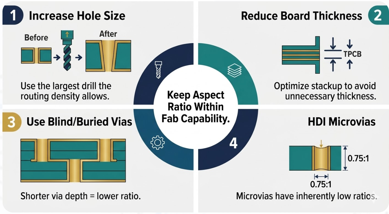
Microvias are based on another logic. Their aspect ratios are, by definition, low because they are only one or two layers (usually 0.05-0.15 mm deep and 0.1-0.15 mm drill diameter). IPC-2226 suggests a ratio of 0.75:1 or less in order to achieve stable fill and stacking of copper microvias with laser drilling.
Factors That Influence Acceptable Aspect Ratio
The maximum aspect ratio your design can safely use is not a fixed number. It shifts based on several interacting factors:
- Material system: Standard FR4 laminates have well-understood drill and plating behavior. High-Tg FR4, polyimide, and Rogers materials each introduce different drill wear rates and desmear requirements that affect final hole quality.
- Board thickness: This is the numerator in the ratio. Thicker boards (driven by layer count, copper weight, or impedance requirements) push the ratio higher for any given drill size. A 10-layer board at 2.0 mm demands larger vias than a 4-layer board at 1.0 mm.
- Drill method: Mechanical drilling handles holes down to about 0.15 mm, but with increasing difficulty below 0.3 mm. Laser drilling produces cleaner microvias at 0.075-0.15 mm but only penetrates one or two dielectric layers.
Design Strategies to Optimize Via Aspect Ratio
Balancing Hole Size, Board Thickness, and Routing Density
The best time to manage via aspect ratio is during stackup definition, not after routing is complete. Once your traces are placed and your vias are locked in, changing drill sizes or board thickness becomes a painful redesign exercise. Here is a practical design playbook:
- Start with your fabricator's recommended via sizes. At JLCPCB, vias with drill diameters of 0.3 mm and above are standard process. Below 0.3 mm, you enter small-hole territory with tighter constraints. Build your via library around these boundaries.
- Challenge your board thickness early. If your 6-layer stackup works at 1.2 mm instead of 1.6 mm, you just dropped the aspect ratio for a 0.2 mm via from 8:1 to 6:1. That is a significant manufacturing improvement with no change to the drill.
- Use the largest drill that your routing density allows. A 0.3 mm drill with a 0.6 mm pad is easy to plate and leaves room for annular ring margin. Reserve 0.2 mm and smaller drills only for the density pinch points where BGA fanout or tight differential pair routing demands it.
Using Blind/Buried Vias to Reduce Aspect Ratio Challenges
A structural solution to routing density when small holes are required, and your board is too thick to allow a comfortable through-hole aspect ratio, is blind and buried vias. These vias do not cross the entire thickness of the board, but rather just a subset of layers, effectively just cutting the depth portion of the aspect ratio equation. Blind vias are used to connect an outside layer to a number of inside layers. The inner layers are linked to one another by buried vias without contacting any surface. Both of these reduce the effective via depth, but with significant tradeoffs:
The cost of the HDI process is high. Blind and buried vias have to be sequentially laminated, i.e., the board is assembled in layers, not drilled and plated at the same time. The cost and lead time increase with every extra lamination cycle. Design complexity rises. You need to specify which layers each via cuts through, registering between lamination cycles, and making sure that your EDA tool is properly set to allocate the vias to the appropriate pairs of layers. DFM involvement should occur at an earlier stage. You cannot afford to complete your stackup isolatedly with HDI builds. Begin working with your fabricator during the schematic phase so that you can be sure that the via structure you intend to implement can be produced at your desired volume and price.
Manufacturing Challenges and Professional Solutions
Plating Uniformity, Void Prevention, and Drilling Accuracy
Reliability via plating depends on a chain of processes, and weakness at any link can compromise the final result. Three process steps are particularly critical for aspect ratio management:
Drilling accuracy sets the foundation. A drill that wanders, creates an oversized or undersized hole, or leaves rough barrel walls creates an uneven starting surface for plating. Drill bit wear, spindle runout, and entry/exit material selection all influence hole quality. For small holes below 0.3 mm, controlled drill parameters and frequent bit changes become essential.
Desmear and etchback prepare the hole for plating. After drilling, resin smear from the laminate coats the inner copper layers, blocking electrical connection. A desmear process (typically permanganate-based) removes this residue. If desmear is incomplete, the plated copper bonds to resin instead of copper, creating a weak interconnect. For high-aspect-ratio holes, the desmear chemistry faces the same transport limitations as plating, making process time and agitation critical.
Electroplating control determines the final copper thickness distribution. Key defect modes and their root causes include:
| Defect | the Root Cause | Aspect Ratio Impact |
| Thin barrel center | Poor throwing power, insufficient agitation | Worsens above 8:1 |
| Mid-barrel void | Trapped air, depleted chemistry | Worsens above 10:1 |
| Barrel crack (post-reflow) | Thin copper + Z-axis CTE mismatch | Risk rises sharply above 10:1 |
| Rough deposit / nodules | Contaminated bath, excessive current density | Indirect, but high AR extends exposure time |
| Knee crack (at layer junction) | Desmear failure + thermal stress | Compounded by deeper holes |
Advanced Techniques for High-Aspect-Ratio Vias
When design constraints demand aspect ratios above 10:1, fabricators turn to advanced process techniques rather than standard DC plating. These approaches improve copper distribution in deep holes, though they add cost. By alternating between plating and deplating current pulses, PPR allows fresh chemistry to replenish inside the hole between deposition cycles. This significantly improves throwing power and can extend reliable plating to 12:1 or higher.
- High-throw electrolyte formulations: Specialized acid copper bath chemistries with optimized brightener, carrier, and leveler additives improve the throwing power of the plating solution without changing the equipment. These chemistries are more expensive but can be qualified for specific aspect ratio ranges.
- Controlled agitation and solution flow: Enhanced solution movement through the holes, via eductor nozzles, panel oscillation, or air sparging, helps overcome mass transport limitations. The goal is to force fresh chemistry into the barrel center and flush out depleted solution.
JLCPCB's Expertise in Managing Via Aspect Ratio
Precision Drilling and Electroplating Capabilities
JLCPCB's published manufacturing capabilities provide a clear framework for designing vias that plate reliably. Here are the key parameters to design around:
- Minimum mechanical drill diameter: 0.15 mm (inner diameter of multilayer boards).
- Minimum via pad diameter: Multilayer boards should have a minimum outer diameter of 0.25 mm, which is sufficient to provide an annular ring after drill registration tolerance.
- Increment of drill sizes: 0.05 mm in the entire interval 0.15 mm-6.3 mm.
- Small hole threshold: Holes less than 0.3 mm in diameter can be defined as small holes and must be controlled more strictly. Above 0.3 mm should be designed where possible, and will save cost and improve yield.
- Board thickness: Standard production is 0.4 mm, 0.6 mm, 0.8 mm, 1.0 mm, 1.2 mm, 1.6 mm, and 2.0 mm.
- Layers supported: 1 to 20 layers.
- Aspect ratio rule: Do not exceed 10:1 when plating through-holes.
JLCPCB also offers via-in-pad (POFV) at no extra charge on 6-20 layer boards. The resin-fill and copper-cap process allows vias to be placed directly under component pads, which is especially useful for the BGA fanout and thermal pad designs where via size and density are constrained.
Reliable Production from Prototypes to High-Volume Runs
- Stackup family standardization: The combinations of common layer counts and thickness have available proven process recipes. When you design in these standard stackups, you get the advantage of thousands of previous production runs of optimizing the process.
- Observed defect trends: These are systematic observations of the various defect rates in plating, such as the distribution of barrel thickness and incidence of voids, so that process drift is detected early enough before it impacts customer yield.
- Prototype-to-production continuity: Boards that were ordered as 5-piece prototypes and then scaled to 10,000-piece production runs have the same process flow. No secret prototype to volume process change.
Starting from $2 for standard PCBs with 1-2 day production times, JLCPCB makes it practical to validate your via design with a small prototype batch before committing to volume. This is especially valuable for designs that approach aspect ratio limits, because a cross-section coupon from the prototype run can confirm plating thickness before you scale up.
Frequently Asked Questions (FAQ)
Q: How do I calculate the via aspect ratio for my design?
Divide your total board thickness by the mechanical drill diameter of the via. For example, a 1.6 mm board with a 0.25 mm drill gives 1.6 / 0.25 = 6.4:1. Always use the pre-plating drill size, not the finished hole diameter, since copper deposition reduces the final hole by approximately twice the plating thickness.
Q: What is the recommended maximum aspect ratio for standard through-hole vias?
Most fabricators reliably plate through-hole vias up to 8:1 using standard processes. Ratios between 8:1 and 10:1 are achievable but may require process validation. Above 10:1, advanced plating techniques are typically needed, and you should confirm capability directly with your manufacturer before finalizing the design.
Q:How does the microvia aspect ratio differ from through-hole via limits?
Microvias are laser-drilled and span only one or two layers, so their depth is much shorter, typically 0.05-0.15 mm. IPC-2226 recommends a microvia aspect ratio of 0.75:1 or lower. This is fundamentally different from through-hole ratios because the plating challenge is proportional to depth, and microvias are shallow by design.
Q: What are the signs that my via aspect ratio is too aggressive?
The most common indicators include intermittent open circuits after reflow, via resistance that increases over thermal cycling, and barrel cracks visible in cross-section. During DFM review, a flag from your fabricator that your drill sizes are below their recommended minimum for your board thickness is an early warning sign.
Q: When should I switch from through-hole vias to blind or buried vias?/h3>
Consider blind or buried vias when your through-hole aspect ratio exceeds 10:1, when you need to route out of fine-pitch BGAs (0.5 mm pitch or below), or when the board thickness is driven by layer count but your via density requires small drills. The decision should be made during stackup definition, not as a late-stage fix.
Popular Articles
• Understanding Electrical Schematics: A Comprehensive Guide
• The Comprehensive Guide to Circuit Symbols: Key to Understanding Electrical and Electronic Diagrams
• PCB Board Design: A Step-by-Step Guide for Beginners
• Choosing the Best PCB Color-Enhancing Aesthetics and Functionality
• PCB Silkscreen: All You Need to Know
Keep Learning
Understanding Electrical Schematics: A Comprehensive Guide
Key Takeaways Schematics vs. Block Diagrams: Schematics detail exact components and connections; block diagrams only show high-level functions. Mark Polarity: Essential to prevent circuit failure and automated SMT placement errors at JLCPCB. Clean Layout: Use modular blocks and net labels (VIN, GND) to eliminate visual clutter. Manufacturing Ready: Follow DFM trace rules and export standard Gerber, BOM (LCSC C-IDs), and CPL files. Fast Troubleshooting: Isolate schematic blocks to test expected voltage......
A Beginner's Guide to Basic Electronic Components: Functions, Symbols & Uses
Every circuit, from a simple LED flashlight to a microcontroller board, is built from the same handful of common electronic components. This guide breaks down the ten basic electronic components you will encounter most often: What each component does How it works Key specifications Where engineers use it By the end, you will be able to recognize these electronic circuit components on a schematic, a PCB, or a parts bin, and know exactly why each one is there. These electronic components are the buildin......
Via Stubs in High-Speed PCB Design: Causes, Effects, and Solutions
Key Takeaways Via stubs are unused via sections that cause reflections, resonance, and jitter in high-speed PCBs. They become critical above 5–10 Gbps; stubs longer than 15 mils (0.381 mm) need mitigation. JLCPCB precision back-drilling reduces residual stubs to under 0.15 mm, greatly improving signal integrity. Optimized stack-up and back-drilling offer the best balance of performance and cost versus blind/buried vias. Choose experienced manufacturers like JLCPCB for reliable high-speed PCB fabricati......
The Comprehensive Guide to Circuit Symbols: Key to Understanding Electrical and Electronic Diagrams
Note Need a quick reference while reading schematics? Download our free, printable Circuit Symbols Cheat Sheet (PDF), featuring the most common IEC and ANSI symbols organized by category. Keep it on your desktop or print it for easy reference at your workbench. ⬇ Download the Free Circuit Symbols Cheat Sheet (PDF) Every electronic diagram is written in a visual language, and circuit symbols are its alphabet. From your first electrical schematic to a multi-layer board, knowing circuit symbols can make ......
Hierarchical Design : Making Complex PCB Projects More Manageable
Key Takeaway Hierarchical design transforms complex PCB projects from overwhelming single-sheet nightmares into well-organized, modular, and manageable systems. By breaking down large schematics into functional blocks with clear interfaces, engineers can significantly improve organization, reduce errors, enhance reusability, and enable smoother collaboration. This approach not only simplifies debugging and layout but also leads to better DFM outcomes and faster time-to-market, making it the preferred ......
Why a Clean PCB Netlist Is the Foundation of Successful Manufacturing
Key Takeaways A clean PCB netlist is the foundation of successful manufacturing, serving as the single source of truth that bridges schematic and physical PCB layout. By ensuring accurate component data, net connections, and version control, it prevents costly errors, improves yield, and enables reliable production. Mastering IPC-D-356 netlist best practices helps engineers reduce risks and achieve high-quality results with JLCPCB. Ever wonder what exactly the link is between your wonderfully drawn sc......