Why Integrated Electronic Manufacturing Matters
15 min
- What Is Electronic Manufacturing?
- From PCB Manufacturing to PCBA
- What to Look for in an EMS Supplier
- Common Challenges in Electronic Manufacturing
- How JLCPCB Simplifies Electronic Manufacturing
- FAQs about Electronic Manufacturing
- Conclusion
Key Takeaways
- Unified Workflow: Combining PCB fabrication, sourcing, and assembly under one supplier removes handoffs and prevents delays.
- Upfront Verification: Early DFM/DFA checks, consistent files, and multi-stage inspections (SPI, AOI, X-ray) eliminate costly rework.
- Seamless Scaling: Keeping prototypes and volume production on one process avoids factory requalification.
- All-in-One Execution: JLCPCB integrates 1–32 layer PCBs, 680K+ parts, and PCBA (2–80,000 boards) in a single order.
Electronic manufacturing involves converting a design into finished electronics: a fabricated circuit board, sourcing components, PCBA assembly and testing, and, in many products, the enclosure around the PCBA. Delays in part delivery, rework, or failed boards indicate a mismatch among the board, parts, and assembly line.
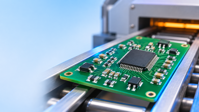
Figure 1: An assembled circuit board leaving an SMT production line
This article will introduce you to electronic manufacturing services (EMS) and explain what makes a bare PCB a PCBA. Next, it explains what to look for in an EMS supplier, what issues delay boards, and why having these stages under one supplier will speed up the journey to working boards.
What Is Electronic Manufacturing?
Electronic manufacturing includes all physical activities from design files to product shipping. The term is for the work itself, and EMS is for a company that does that work for you.
Electronic Manufacturing vs. Electronic Manufacturing Services (EMS)
The activity is electronic manufacturing: fabricating boards, placing and soldering components, testing assemblies, and building them into products. Electronic manufacturing services (EMS) is a business model in which a third-party company performs manufacturing for another company. That customer is typically the original equipment manufacturer (OEM) who owns the design and markets the product as their own. An EMS supplier with multiple customers sharing the amortization of placement machines, reflow ovens, and test equipment has many OEMs outsourcing some or all of the work.
| Aspect | Electronic Manufacturing | Electronic Manufacturing Services (EMS) |
|---|---|---|
| What it describes | The process of building electronics | An outsourced service that runs that process |
| Who owns the design | Whoever builds the product | The customer (OEM); the supplier builds to its files |
| Typical scope | Fabrication, assembly, test, final assembly | Anything from assembly only to sourcing, test, box build, and logistics |
The word "EMS" on a quote does not define the scope; the contract does. Confirm which stages a supplier actually covers before comparing prices.
Key Stages of the Electronic Manufacturing Process
Most electronic products pass through the same eight stages, whether one company runs them all or several suppliers split them:
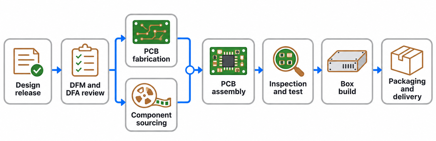
Figure 2: The electronic manufacturing process from design files to shipped product
- Design release: The schematic, PCB layout, and manufacturing files are frozen at one revision.
- DFM and DFA review: The fabricator and assembler check the files against their process limits before anything is built.
- PCB fabrication: The bare board is made from Gerber or ODB++ data, drill files, and the stackup.
- Component sourcing: Parts are purchased per the bill of materials (BOM), with approved alternates when a part is in short supply.
- PCB assembly: Components are placed and soldered by SMT and, where needed, through-hole processes.
- Inspection and test: Optical, X-ray, electrical, and functional checks confirm the assembly works.
- Box build: The PCBA is installed in its enclosure with cables, displays, and power supplies.
- Packaging and delivery: Finished units are packed, labeled, and shipped.
Fabrication and sourcing run in parallel and meet at assembly, so the slower of the two sets the day the build can start. That is the first reason integration matters. When one supplier owns both streams, a late board or a missing part is visible before the line is booked, not on the day the boards are due.
From PCB Manufacturing to PCBA
A bare PCB is the interconnect structure made of copper laminate, plated-through holes, and solder mask, without components. That board with all the parts soldered in is a PCBA, and the transition from the board to a PCBA involves three workflows: board, parts, and assembly line.
PCB Fabrication and Material Selection
PCB manufacturing uses copper-clad laminate cores and prepreg sheets to create the board. The copper on each core is patterned and etched onto an inner-layer pattern. The layers are then pressed together with prepreg, drilled, and plated, with the holes providing the connection; the outer layers are then imaged and etched. Next, the solder mask, surface finish, and silkscreen are added, and an electrical test is performed to verify each net before assembly.
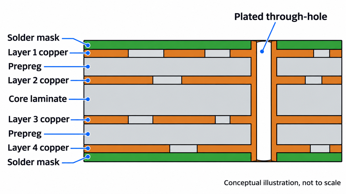
Figure 3: Cross-section of a four-layer board built from cores and prepreg
The type of material determines the board's survival during assembly. The decomposition temperature and time to delamination on the laminate datasheet are important as well because standard FR-4 has a glass transition temperature (Tg) typically around 135-140 °C; above Tg, the resin expands quickly, so boards that experience several reflow passes with lead-free solder or have high laminate counts often move to higher Tg grades rated at 155 °C or 170 °C. When FR-4's dielectric loss is the problem, RF boards move to low-loss laminates.
PCB Assembly and SMT Processes
The main technique of the PCB assembly process is surface-mount technology (SMT). Using a stencil, solder paste is applied to the pads and then inspected with solder paste inspection (SPI) to measure each deposit. Then, pick-and-place machines place each part onto its paste, and a reflow oven fuses the paste into joints. Automated optical inspection (AOI) tests for placement, polarity, and visual joints. Connectors and large capacitors, etc., are added later by wave soldering, selective soldering, or hand soldering.
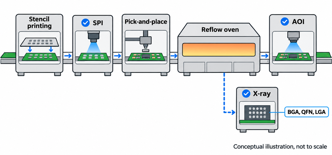
Figure 4: SMT assembly line with its inspection points
A large number of assembly defects begin at the paste print, since the amount of solder each joint receives is determined by the stencil. If too little paste is used, the joint is open or weak; if too much is used, bridges or solder balls form. This is why the line measures paste before placing it, rather than waiting for AOI to find the result. Some packages cannot be inspected with a camera, such as BGA, QFN, and LGA, and must be inspected with X-ray.
Component Sourcing and Supply Chain Coordination
Sourcing turns the BOM into parts at the placement machine. Every line needs a manufacturer part number, a quantity that accounts for reel attrition, and, ideally, an approved alternate. The parts must also arrive in a form the line can use, because placement machines feed from reels or trays. Moisture-sensitive packages are also tracked, so they can be baked if they have been exposed for too long. Who buys the parts is set by the sourcing model.
| Model | Who Buys the Parts | Suits | Main Risk |
|---|---|---|---|
| Consigned | You supply every part | Custom or already-stocked parts | A short or wrongly packed part stops the build |
| Partial turnkey | The assembler buys most; you supply a few | BOMs with a few special parts | Two delivery schedules must meet |
| Full turnkey | The assembler buys every part | Standard parts and fast builds | Less control over part lots |
What to Look for in an EMS Supplier
An EMS supplier is chosen on evidence: what its lines can build, how it proves quality, and how it handles time and change. A low unit price means little if the boards arrive late or fail incoming inspection.
Manufacturing Capabilities and Technical Support
Start by matching your design to the supplier's published limits. Check the layer count, minimum trace and space, smallest drill, surface finishes, smallest placeable package, finest BGA pitch, and whether it assembles both sides. A design that sits at the edge of one limit usually builds, but often at lower yield, so the margin below the limits is worth more than a single headline number.
Technical support is the second test. A good supplier returns a DFM and DFA report before production, listing each problem and its fix. Catching a pad too close to the board edge or a missing fiducial at that point costs a file change instead of reworked boards. Ask how engineering change orders (ECOs) are handled once production has started, because a supplier without a defined change process slows every revision.
Quality Control and Production Consistency
Quality control is proven with certificates and data, not claims. Ask for the supplier's ISO 9001 certificate and any sector-specific certificates required for your product, such as ISO 13485 for medical devices. Then ask which IPC-A-610 class it builds to, since that standard sets the acceptance criteria for electronic assemblies. Measured first-pass yield, on-time delivery, and return rates indicate whether the system works, whereas a certificate only proves that a quality system exists. Consistency comes from inspecting at each stage where a defect can hide.
| Method | Where It Runs | What It Finds | What It Misses |
|---|---|---|---|
| SPI | After stencil printing | Paste volume, height, offset, and bridging | Placement and joint defects |
| AOI | After placement or reflow | Missing, shifted, or reversed parts; visible solder defects | Joints hidden under packages |
| X-ray | After reflow, on BGA, QFN, and LGA | Voids, bridges, and opens under the body | Functional faults |
| Functional test | After assembly | Whether the board does its job | The root cause of a failure |
Lead Time, Cost, and Order Flexibility
The lead time is determined by the slowest of three clocks – board fabrication, parts procurement, assembly. Request the supplier's assembly quote individually – a quick assembly quote is worth nothing if one of the BOM parts has a long lead time. Inquire about expediting charges as well, as the build time for an expedited build is typically longer.
Look at cost per working board, NOT unit cost. Setup, stencil, and tooling costs are major items for small orders and diminish at volume, while scrap, rework, and late-delivery costs are not included in the quote. It is complemented by order flexibility. The prototype files are transferred directly into production when a supplier builds 5 boards and 5,000 boards on the same process without having to qualify a new factory.
Common Challenges in Electronic Manufacturing
The three most common causes of failed or late builds are: unavailable parts, designs that cannot be built cleanly on the line, and late detection of defects. Each is less expensive to correct in the design than on the line.
Component Availability and Sourcing Risks
A part on the BOM can become unavailable at any point in a product's life. Manufacturers usually mark a part as not recommended for new designs (NRND) before declaring end of life (EOL) and offering a last-time buy. Shortages can also stretch lead times on parts that are still active. Check the lifecycle status of every line before releasing the design, because a part change after layout means a board revision. Where the circuit allows it, choose parts with drop-in alternates from other manufacturers.
The second risk is counterfeit or mishandled parts, which enter the supply chain when parts are bought from unverified brokers to cover a shortage. Buying through the manufacturer or its authorized distributors and maintaining lot traceability is the main defense, because every part can then be traced to its original manufacturer.
PCB Design and Assembly Compatibility
A board can pass every electrical check and still be hard to build. Design for manufacturing and assembly (DFMA) closes that gap by checking the layout against the assembler's process before release. The common problems are pads that differ from the footprint specified in the part's datasheet and missing fiducials. Parts placed too close together cause trouble too, because the placement nozzle and the rework tool both need room.
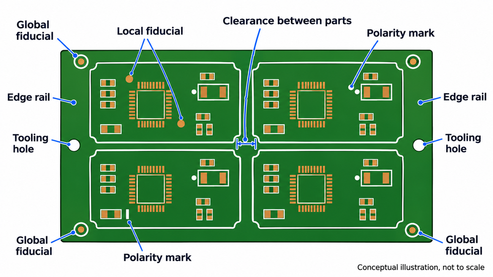
Figure 5: Assembly features an assembler needs on a PCB panel
Panelization is where the layout meets the line. The assembler needs edge rails for the conveyor, tooling holes to register the panel, global fiducials for the placement camera, and local fiducials beside fine-pitch parts. Clear polarity marks in the silkscreen let AOI and operators confirm orientation. Matching each footprint to the exact part on the BOM, rather than just its package name, prevents errors from parts that share a package but not a pinout.
Quality Issues and Production Delays
Quality problems and delays are frequently a defect twice over: a defect found late requires rework, and the rework pushes the ship date. The common SMT defects are solder bridges, opens, tombstoned passives, and voids under thermal pads. The majority of these are related to stencil design, stencil footprint, or reflow profile. The fix should be in the files or process, not rewriting boards one at a time.
The file package is also experiencing delays. An incomplete BOM prevents a build from completing the engineering review process, and a placement file that does not match the footprints or a Gerber revision that is not in sync with the BOM also halts a build. The release of a single controlled package, which is checked for consistency across files, helps keep the next build on schedule, since the assembler has nothing to query.
How JLCPCB Simplifies Electronic Manufacturing
JLCPCB handles PCB fabrication, parts sourcing, and PCBA in a single order, so the board, parts, and assembly are scheduled together. That removes the handoffs between separate suppliers, where many of the delays above begin.
Integrated PCB Fabrication and Assembly Services
JLCPCB's published PCB capabilities cover FR-4 boards from 1 to 32 layers, plus aluminum-core, copper-core, and Rogers or PTFE RF boards; the same order can include assembly. Economic PCBA places parts on one side, down to 0402, for 2 to 50 boards with a build time of 1-3 days. Standard PCBA places both sides, down to 01005, for 2 to 80,000 boards, and adds SPI to the inspection flow.
Both services take the AOI, and X-ray is applied automatically to BGA, QFN, and LGA packages and is quoted as a cost. Wave soldering for through-hole parts is done in the same order. Free DFM and DFA checks are performed before production, and power-on or functional test can be performed to your requirements. Get an instant quote by uploading your Gerber, BOM, and placement files.
Global Component Sourcing and Supply Chain Support
The parts library contains over 700,000 parts in stock, and BOM matching against it provides availability before placing the order. A part outside the library is available for purchase via global sourcing from trusted distributors with a lead time of 9-15 days, or by you. Parts can also be pre-ordered into a private library for use in a later build, rather than being purchased again for each order when they are scarce and/or have a long lead time.
From Prototyping to Scalable Production
Prototyping and production prove different things. A prototype build proves the design works, and a pilot build proves the process, the test coverage, and the yield. Volume production then adds change control, traceability, and statistical monitoring, so every unit matches the approved build. A problem found at the pilot stage costs a file change, while the same problem found in volume costs scrap.
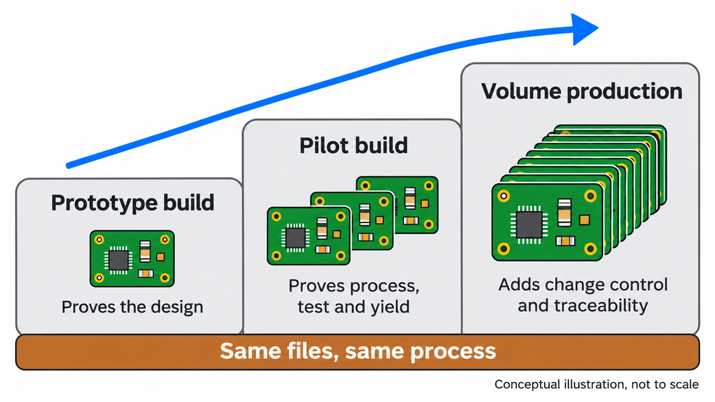
Figure 6: What each build stage proves on the way to volume production
Keeping all three stages with one supplier and one process means the prototype's DFM fixes, footprint corrections, and placement data carry over unchanged. Standard PCBA at JLCPCB covers 2 to 80,000 boards, so files approved on the prototype can be reordered at volume without qualifying another assembler.
FAQs about Electronic Manufacturing
Q: What is the difference between an EMS supplier and an OEM?
An OEM owns the product design and sells the product under its own brand. An EMS supplier builds that product, or its assemblies, to the OEM's files and specifications. The OEM stays responsible for the design, and the EMS supplier for artistry and the manufacturing process.
Q: What files does an EMS supplier need to quote a PCBA order?
Gerber or ODB++ files with drill data for the bare board, plus a BOM with manufacturer part numbers. A placement (centroid) file gives each part's position and rotation. Assembly drawings, polarity notes, and test requirements let the supplier quote accurately without follow-up questions.
Q: Which IPC-A-610 class should I specify?
Class 2 suits most commercial and industrial products, where long service life is expected but cosmetic imperfections are acceptable. Class 3 is for high-reliability equipment, such as medical or aerospace hardware, that must work every time. Class 1 covers general products where basic function is the main requirement.
Q: What is NPI in electronic manufacturing?
NPI, or new product introduction, is the process of moving a new design into production. It covers DFM review, prototype and pilot builds, test development, and process qualification, so the first production run uses a proven process instead of discovering problems at volume.
Q: What is box build assembly?
Box build is the stage after PCBA in which the assembled board is installed in its enclosure with cables, wiring harnesses, displays, power supplies, and labels. The result is a finished unit, usually tested as a complete system before it ships.
Conclusion
Treat electronic manufacturing as one connected process, not a set of separate purchases. The board, the parts, and the assembly must agree on one revision of the files, and every handoff between suppliers is a chance for them to disagree. Choose an EMS supplier based on published capabilities, inspections at each stage, and verifiable lead times, then keep the same process from prototype to volume. JLCPCB combines fabrication, sourcing, and assembly into a single order, so upload your design to get an instant quote for your PCBs and PCBA.
Popular Articles
• The Hardware Development Process: From Concept to a Finished Electronic Product
• Understanding the Basics of Electronic Devices and Circuits
• Understanding Digital Circuit Timing: Setup Time, Hold Time, Contamination Delay & Clock Skew
• PCBs Explained: A Simple Guide to Printed Circuit Boards
• Guide to the Top 10 Commonly Used Electronic Components
Keep Learning
A Beginner's Guide to Printed Circuit Board Repair: Common Issues, Methods, and Solutions
Key Takeaways Understand PCB structures, components, and common failure causes to identify repair challenges effectively. Follow a systematic PCB repair process, from fault diagnosis and component replacement to testing and verification. Know when PCB repair is practical and when remanufacturing a new PCB provides a more reliable solution. A printed circuit board (PCB) is a critical part of almost every electronic device. When a board fails, the problem may come from damaged components, broken copper ......
What is PCB Via and Which Type Should You Choose?
Printed Circuit Board (PCB) design is a critical aspect of electronic product development. PCBs provide an organized and compact layout for electronic components, enabling efficient signal transmission and minimizing the risk of electrical interference. One essential element of PCB design is the via, a small hole drilled into the board that allows electrical connections between the different layers of the board. In this article, we will provide a comprehensive overview of PCB via, including its types,......
Optimize PCB Trace Spacing for High-Performance PCBs
Key Takeaways Trace Spacing vs. Clearance: Trace spacing is the edge-to-edge distance between copper conductors on the same layer, while clearance encompasses the broader safety envelope between traces and non-trace features like board edges and mounting holes. The 3W Rule: For high-speed signals, maintain at least 3x the trace width between centerlines (2W edge-to-edge spacing) to reduce crosstalk by up to 70%. IPC-2221 Standards: Industry-standard clearance values depend on voltage levels, altitude,......
PCB Board Outline: Smart Design Tips for Seamless Manufacturing
Key Takeaways Board Outline Defined: The closed polygonal contour on Mechanical Layer 1 that defines your PCB's final physical boundary, including cutouts, slots, and mounting holes. Why It Matters: Directly impacts enclosure fit, mechanical stability, assembly efficiency, and production yield — a well-designed outline reduces costs and lead times. Critical Parameters: Maintain ≥0.2 mm edge clearance, use ≥0.5–1.0 mm corner radii, and specify tolerances appropriate to your routing method (±0.1 mm prec......
Why Integrated Electronic Manufacturing Matters
Key Takeaways Unified Workflow: Combining PCB fabrication, sourcing, and assembly under one supplier removes handoffs and prevents delays. Upfront Verification: Early DFM/DFA checks, consistent files, and multi-stage inspections (SPI, AOI, X-ray) eliminate costly rework. Seamless Scaling: Keeping prototypes and volume production on one process avoids factory requalification. All-in-One Execution: JLCPCB integrates 1–32 layer PCBs, 680K+ parts, and PCBA (2–80,000 boards) in a single order. Electronic m......
PCB Layers Explained : Building Better Boards Through Smart Stackup, Standards, and Design Practices
A PCB is a sandwich of copper and insulating sheets that are stacked together to form a circuit board. Each PCB layer has a specific purpose; for example, some carry signals (traces connecting components), while others serve as solid planes for power or ground. Think of PCB layers like the floors in a building, where each floor can have a different role. Think of it as offices (signals) on one floor and storage (ground/power) on another. The number of layers varies by design complexity, from just one ......