
Hard Gold PCB Finish: Achieving Exceptional Wear Resistance and Contact Performance
13 min
- Hard Gold vs. ENIG and Soft Gold: Key Distinctions
- Design Considerations for Optimal Hard Gold Implementation
- Precision Manufacturing of Hard Gold Finishes
- JLCPCB's Mastery in Delivering High-Quality Hard Gold PCBs
- Frequently Asked Questions (FAQ)
Surface finishes are not all the same thing, and this is obvious beyond mention when you are dealing with parts that are beaten against one another over and over. Hard gold. The most common finish used when PCBs must complete hundreds or even thousands of insert-and-remove operations before going out of service is essentially a hard alloy of gold electroplated over a nickel barrier coating. The prototypical piece of evidence that demonstrates why this is important is the edge connector, otherwise known as a gold finger. These miniature card edge contacts are inserted into similar connectors on motherboards, backplanes, and test boards, and each time they collide with something, they receive a bit of abrasion.
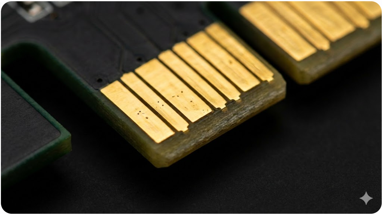
With a typical ENIG finish (that thin 0.05 - 0.1 micrometer gold plating), you would get the gold to wear away in only a couple of dozen insertion cycles, revealing the nickel metal underneath it, then copper. The result of that is increased contact resistance, oxidation, and bizarre connection failures. Hard gold fixes, which are made hard by a much thicker gold layer (typically 0.5-1.5µm, sometimes up to 2.5µm) mixed with a small amount of cobalt or nickel. This thickness and hardness combination enables hard gold contacts to pass through 500-1000+ insertion cycles and maintain the contact resistance low and constant throughout the entire life of the part. Other typical applications are membrane keypad contacts, test-point pads on bed-of-nails fixtures, slider contacts in potentiometers and switches, and anywhere there is a contact surface that rubs or abrades back and forth.
Applications Requiring Superior Durability Over Standard Finishes
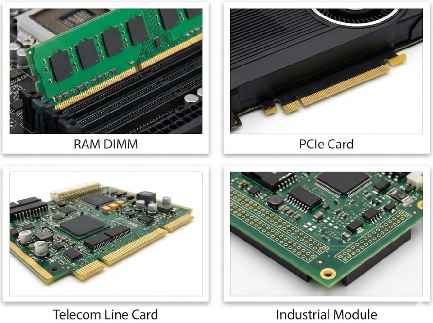
In addition to the insertion connectors, hard gold is required in cases where the reliability of contacts during mechanical stress is required over a long period. The card cage architecture of industrial control systems utilises gold finger edge connectors that are required to be serviceable over a 15-20 year period of periodic maintenance and reconfiguration. Test and measurement equipment is based on gold-plated test points and probe pads, which are required to sustain a constant level of contact resistance over millions of test cycles.
Field-replaceable modules, such as line cards, switching modules, optical transceivers, etc., are provided with edge connectors. The life of the contact surface finish in any of these applications is directly related to system reliability and the cost of maintenance. Hard gold is also being used in high-reliability connector contacts in safety-related systems in the automotive industry. The electronic control units (ECUs) of the braking, steering, and powertrain cannot withstand the contact degradation throughout the lifetime of the vehicle, and hard gold is a reasonable investment in spite of its high price.
Hard Gold vs. ENIG and Soft Gold: Key Distinctions
Thickness, Hardness, and Brittleness Trade-Offs
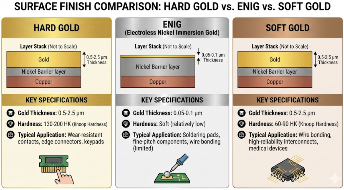
When choosing a finish on your board, you must be conversant with hard gold, ENIG, and soft gold. ENIG, which is an abbreviation of Electroless Nickel Immersion Gold, deposits a small gold layer (0.05-0.1µm) over a 3-6µm nickel layer. That gold is soft and pure, and it has the primary purpose of covering the nickel prior to you soldering. ENIG is a good choice in case you are soldering flat parts, but you cannot expect it to be the least wear-resistant; that thin layer of gold will be all but worn away after even a few blows.
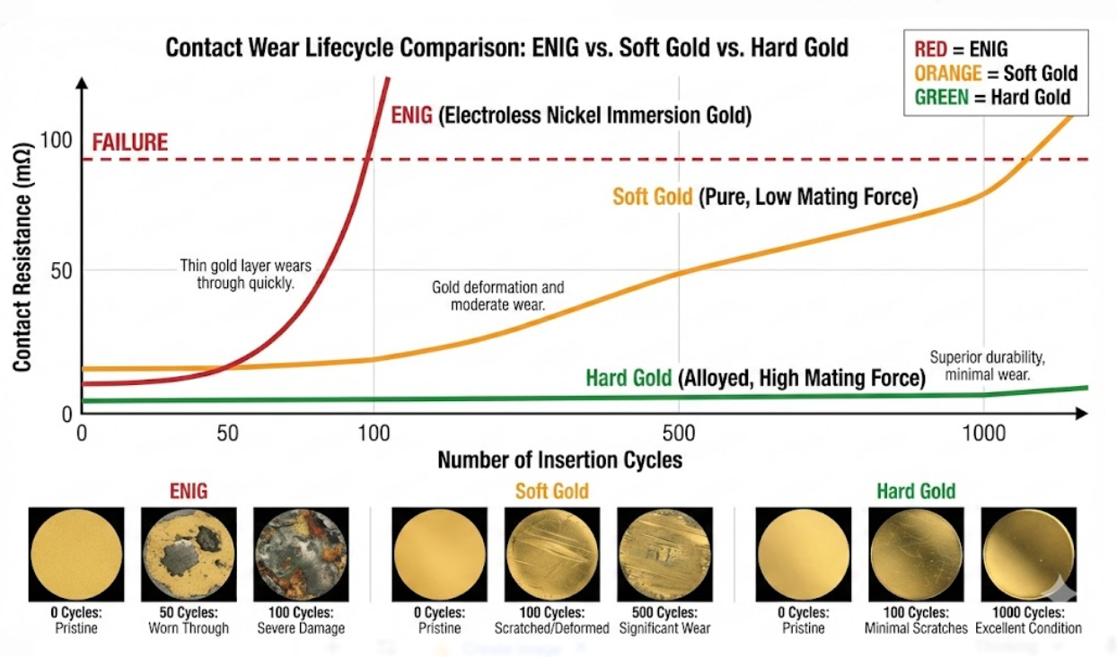
Soft gold (also known as bondable gold or Type III gold) is actually gold electroplated; it is nearly 100 percent pure (99.7 percent+). It is normally 0.5-2.5µm, and it is super ductile, which is why it is ideal to use in wire-bonding, whereby the tool is required to dent the gold to establish a connection. The flip side? It is not good in sliding contacts since it is easy to wear out due to low hardness (60-90 HK).
A different beast is hard gold - Type I or Type II. It is electroplated gold with a trace of cobalt or nickel (0.1 -0.3%), which results in a final hardness of 130-200 HK Knoop. The wear resistance is terrific with that hardness increase, and yet conductive. The thing about it is that once you exceed 2.5µm in thickness, the layers may become brittle and fracture when they are stressed.
Electroplated Process Advantages for Wear Resistance
The electroplated nickel-gold method (or electrolytic nickel-gold), which produces hard gold, is in fact superior to the chemical (electroless) one. When you need it, you can have uniform coatings down to 0.25 - 2.5 µm thick with electroplating by simply varying the plating time and current density to get the desired thickness. The nickel underlayer (typically 2.5-5.0µm) serves as a diffusion barrier to prevent copper from entering the gold, and also provides a hard substrate, such that the gold layer will not deform due to contact pressure.
It is also selective, gold only forms where there is a linkage to the plating bus (the current-carrying traces that are between the plating pads and the panel edge as you make the board). That allows hard gold on edge connectors and another finish, such as ENIG or some other finish, on the soldering pads in the same board, so each area is optimized to its purpose.
Pro-Tip: When specifying hard gold, always indicate the gold thickness, nickel thickness, and plating area clearly in your fabrication notes and drawing. Ambiguous specifications lead to incorrect plating thickness or plating on the wrong areas, both expensive mistakes to correct.
Cost and Performance Comparisons in Real Projects
The ENIG vs hard gold cost comparison is stark. ENIG typically adds 5-15% to the bare board cost, while hard gold on edge connectors can add 20-50% or more, depending on the plating area and gold thickness. The gold material cost alone is high, as gold pricing fluctuates with commodity markets, and thicker plating means proportionally more gold consumed. However, the cost comparison must account for the application’s lifetime requirements. A server backplane with 50 line card slots, each requiring 500+ insertion cycles over a 10-year service life, has no economically viable alternative to hard gold.
The cost of field failures from worn contact surfaces (technician dispatch, downtime, replacement parts) vastly exceeds the premium for hard gold plating. For designs with minimal insertion requirements (fewer than 20 cycles), ENIG or even OSP may suffice. The decision should be driven by a realistic assessment of the contact’s lifecycle mechanical demands, not by default specification.
Design Considerations for Optimal Hard Gold Implementation
Finger Spacing, Beveling, and Plating Area Definition
Gold finger design follows specific rules to ensure reliable mating and long-term performance. Finger width and spacing must match the mating connector specification precisely. Standard edge connector pitches include 1.27mm (50 mil), 1.0mm, and 0.8mm for high-density applications.
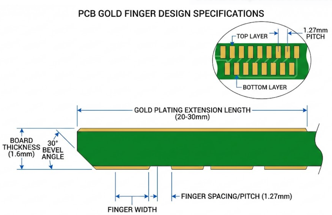
Beveling is chamfering the board edge at a 30-45 degree angle that facilitates smooth insertion into the mating connector and reduces the initial contact force that can damage the gold surface. Most gold finger designs specify a 30-degree bevel on the insertion edge.
Plating area definition requires careful attention. The gold must extend far enough from the board edge to maintain contact with the connector throughout the full insertion depth, but should not extend unnecessarily because every additional square millimeter of gold plating adds cost. A typical gold finger extends 20-30mm from the board edge, depending on the connector specification.
Avoiding Brittleness Issues Through Proper Thickness Control
The largest thing we need to look out for in hard gold projects is gold brittleness. When we make it too thick, say more than 2.5 μm thick, it may develop internal stresses and crack, especially along sharp corners or edges. The hardening cobalt or nickel that provides the hardness also decreases the ductility; therefore, we have a sweet spot of thickness that is optimal between wear resistance and mechanical integrity.
Most edge connector material takes 0.75-1.5µm of hard gold over 2.5-5.0µm of nickel to strike that sweet spot. The combination of that can be repeated thousands of times and remain soft enough to prevent cracking during flex-folding or heating of the board. Should we require the stuff to be extreme-duty, such as exceeding 1,000 cycles, we may increase the gold to 2.0 - 2.5 µm, but we certainly must not allow it to go around sharp geometry transitions, which would accumulate stress.
Integration with Overall PCB Layout and DFM Rules
Hard gold areas require special consideration in the overall PCB layout. Plating bus traces must connect all gold finger pads to a common plating rail during fabrication. These traces are typically routed on the same layer as the gold fingers and are removed (by routing or scoring) after plating is complete. The designer must plan for these temporary connections in the layout. Solder mask must be carefully defined to expose only the intended gold plating areas while protecting adjacent features.
Soldermask-to-gold registration tolerance is critical mask overlap onto gold fingers creates insertion interference, while excessive gap exposes copper that can oxidize. DFM review should verify that gold finger dimensions match the target connector specification, bevel dimensions are correctly defined, plating bus routes are feasible, and the transition zone between gold-plated and non-gold-plated areas is properly managed.
Precision Manufacturing of Hard Gold Finishes
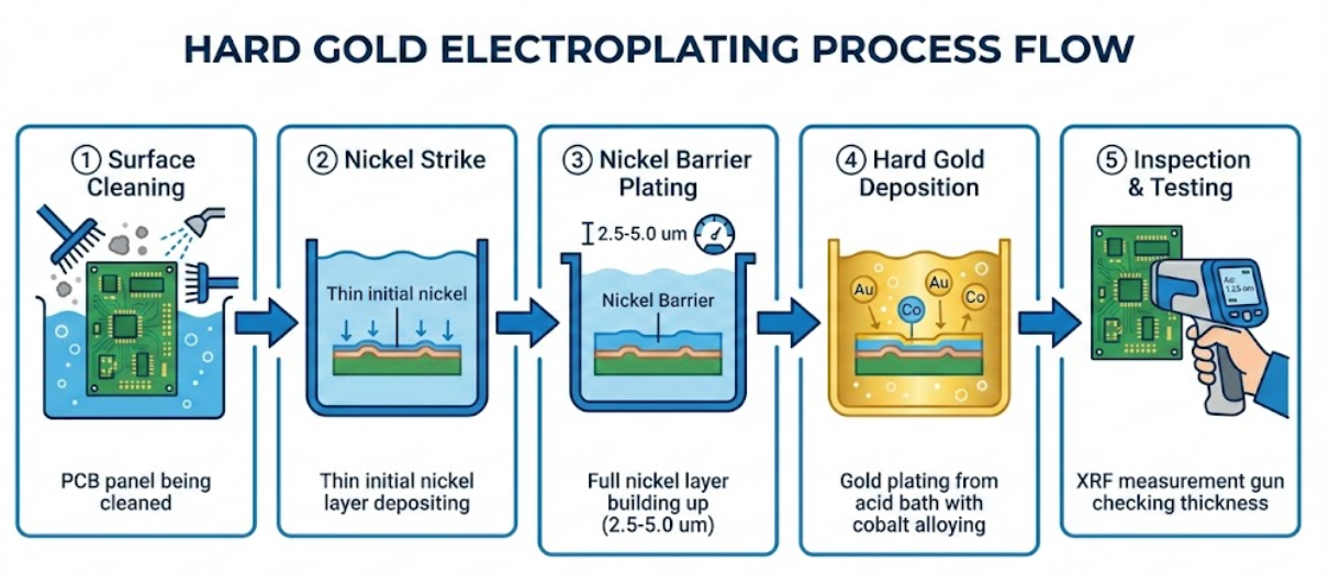
Electroplating Nickel Barrier and Gold Layer Deposition
Basically, therefore, the entire hard gold thing begins when all the rest on the board is finished. We need to clean up the copper first, and then we have to plate it. Laying down a nickel strike layer, then immediately followed by the main nickel barrier (approximately 2.5-5.0mm of sulfamate nickel). That provides the board with a hard base and prevents diffusion.
When the nickel is in, we shift out to the gold. It is produced out of an acid gold bath containing cobalt or nickel. We monitor the present density, bath temperature, and agitation extent of the stuff, so the gold is hard enough and the grains. We check it using coulometric measures of thickness to ensure that the gold finishes the correct thickness in all locations.
Uniformity Control and Post-Process Cleaning Techniques
It is hard to make the gold smooth on all the fingers of a panel. The edges and angles are more likely to be struck by the current (that is, the dog-boning thing), and in those places, the thickness is much greater than the thickness in the middle. To correct that, the plating shops are equipped with additional anodes, current thieves, and intelligent rack constructions to distribute the current and ensure that the thickness difference is minimal.
We then plate, and we clean the board to remove any remaining chemicals, flux, and contamination that may interfere with the contacts. An ultrasonic clean followed by a deionized water rinse. We then examine the gold with a magnifier, looking at it to see whether it has pitting, nodules, staining, and general dirt.
Rigorous Testing for Adhesion, Hardness, and Contact Resistance
We test hard gold in a number of tests when we check it. The X-ray fluorescence (XRF) tests the validity that the gold and nickel layers have reached the minimum and maximum thicknesses at various points. The tests of microhardness of the knoop ensure that the alloy of gold is flattened into 130-200 HK.
An adhesion test (tape test according to IPCTM650) is also done to ensure that the gold and nickel actually adhere to each other and to the copper. It is also measured by the contact resistance, and it must be low and uniform- this is essential in a sound electrical contact. These tests are performed on actual production samples and coupons in order to ensure that each batch is spec-matched.
JLCPCB's Mastery in Delivering High-Quality Hard Gold PCBs
Advanced Electroplating Lines for Consistent Thickness and Durability
JLCPCB’s electroplating facility includes dedicated hard gold plating lines with precision current control, automated thickness monitoring, and optimized bath chemistry. These systems deliver consistent gold thickness and hardness across panels, ensuring reliable contact performance for every board in every order.
Expert Support for Custom Gold Finger Specifications
Specifications of the gold finger could differ tremendously based on the connector standard and what your project requires. The engineering team at JLCPCB is on hand to assist with special orders - need some bizarrely thin gold, a very specific nickel undercoat, a patch of selective plating, or a little extra-beveling. They can flex to accommodate one, should you be doing a PCIe card edge spec, or an entirely new proprietary interface.
Reliable Production Ensuring Long-Term Contact Performance
They are not new to hard gold plating, and they have been involved with all the consumer-level and industrial-level backplanes. All boards they ship pass through the same stringent quality check, such as the XRF thickness checks and the eye check, thus you can be sure that the contacts remain solid throughout the product's life.

Frequently Asked Questions (FAQ)
Q. What is the difference between hard gold and ENIG?
ENIG deposits a thin (0.05-0.1µm) soft gold layer over nickel using a chemical process. Hard gold electroplates a much thicker (0.5-2.5µm) cobalt-alloyed gold over nickel using electrical current.
Q. How many insertion cycles can hard gold withstand?
Properly specified hard gold (0.75-1.5µm over 2.5-5.0µm nickel) typically survives 500-1,000+ insertion cycles. Thicker gold (up to 2.5µm) can extend this further.
Q. Can hard gold and ENIG coexist on the same board?
Yes, this is common practice. Hard gold is applied to edge connectors and contact areas, while ENIG covers the soldering pads. The selective plating process deposits gold only on areas connected to the plating bus, allowing different surface finishes on the same board.
Q. Is thicker gold always better for hard gold applications?
No. Excessively thick hard gold (above 2.5µm) can become brittle and prone to cracking. The optimal thickness depends on the expected number of insertion cycles and the mechanical stress environment.
Q. Why is hard gold more expensive than other surface finishes?
Hard gold cost is driven by the gold material itself (commodity-priced precious metal), the thicker deposition (10- 50x more gold than ENIG), and the electroplating process requiring dedicated equipment and precise control.

Keep Learning
Conformal Coating in PCB Technology: Benefits, Challenges, and Future Developments
If you're searching for conformal coating, you're likely looking for a reliable way to protect your PCB from moisture, dust, chemicals, or harsh environments. Choosing the right coating directly affects product reliability, performance, and lifespan. In this guide, you'll learn what conformal coating is, the main types available, and how to select the best option for your application. We'll also cover key benefits, application methods (manual, automated, and selective), as well as inspection, rework, ......
Preventing Black Pad Defects: Ensuring Reliable ENIG Finish in Professional PCB Manufacturing
Key Takeaways Black Pad is caused by excessive nickel corrosion during the ENIG immersion gold step, leading to brittle solder joints and hidden BGA/QFN failures. Key prevention methods: tight chemistry control (temperature, pH, time), consistent phosphorus content, and regular bath monitoring. High-reliability alternatives: ENEPIG (lowest risk) or nickel-free finishes like Immersion Silver and OSP. Always source ENIG from manufacturers with strict process controls. Ever get a great-looking board, wor......
Solder Mask Colors: Boost Your PCB Performance, Style & Reliability
Key Takeaways Solder mask color directly impacts AOI accuracy, thermal performance, and PCB reliability — it is not purely cosmetic. Green remains the industry benchmark for the highest manufacturing yields and fastest turnaround at no extra cost. White maximizes light reflection for LED applications, while black offers a premium aesthetic for high-end consumer products. Red and yellow provide superior visual contrast for prototyping, debugging, and safety-critical inspections. JLCPCB offers all seven......
Why Copper Oxidation Matters in PCB Design & How to Prevent It
Key Takeaways Copper oxidation is a critical concern in PCB design that directly impacts solderability, contact resistance, and long-term reliability. By understanding how oxidation forms and damages copper surfaces, designers can effectively prevent it through appropriate surface finishes (such as HASL, ENIG, and OSP), strategic solder mask application, and strict adherence to proper storage and handling practices per IPC-1601 guidelines. Protecting copper from oxidation ensures better assembly yield......
Comparing OSP Plating with Other PCB Surface Finishes
Key Takeaways OSP stands out as a cost-effective, ultra-flat, and environmentally friendly PCB surface finish with excellent solderability for fine-pitch components, making it ideal for high-volume consumer electronics. However, its short shelf life (3–6 months), sensitivity to handling and oxidation, and limited multi-reflow durability require careful storage and process control. When compared to HASL, ENIG, Immersion Silver, and Immersion Tin, OSP offers superior planarity and lower cost but trades ......
Hard Gold PCB Finish: Achieving Exceptional Wear Resistance and Contact Performance
Surface finishes are not all the same thing, and this is obvious beyond mention when you are dealing with parts that are beaten against one another over and over. Hard gold. The most common finish used when PCBs must complete hundreds or even thousands of insert-and-remove operations before going out of service is essentially a hard alloy of gold electroplated over a nickel barrier coating. The prototypical piece of evidence that demonstrates why this is important is the edge connector, otherwise know......