Key Benefits of In-Circuit Test in High-Yield PCB Manufacturing
17 min
- Fundamentals of In-Circuit Testing
- Fundamentals of In-Circuit Testing
- Top Advantages of In-Circuit Test for Quality Control
- DFM Requirements for Successful ICT Coverage
- Our Professional Testing Capabilities for Zero-Defect Delivery
- FAQs About In-Circuit Test
- Conclusion
Key Takeaways
- Precise Faults: ICT tests individual components to report exact pin-level failures without booting firmware.
- Layout-Driven: Coverage depends on layout rules like test pad size (0.9-1.0 mm), pitch, and clearances.
- Fixtures vs. Probes: Bed-of-nails runs in seconds for high volume; flying probes require zero tooling for prototypes.
- Guarded Accuracy: Guarding isolates components from parallel paths to detect bad values early and lower rework costs.
- Layered QA: Combining ICT with AOI and AXI delivers full coverage across assembly.
An in-circuit test checks the parts on an assembled board one at a time, through spring pins pressed onto the copper. A whole board takes seconds. It does not care whether the firmware boots, because it asks a narrower question: is every part the right value, the right way round, and soldered to the right nets? A failed functional test tells you the board is dead, whereas a failed in-circuit test names the joint: R14 reads open, or two pins of U3 are bridged. Each of those measurements needs a pad that the probe can reach.
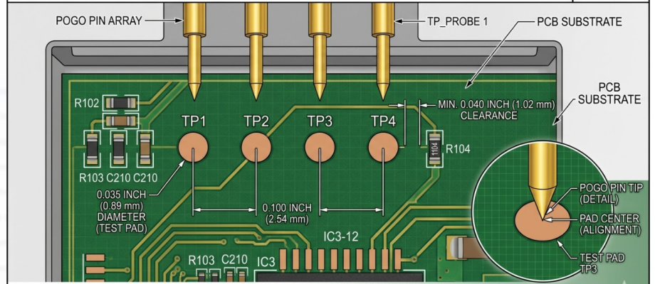
Figure 1: An assembled PCB pressed onto bed-of-nails spring probes
So the coverage you get is decided in layout, long before anyone builds a fixture. This guide covers how ICT runs in production and how bed-of-nails fixtures compare with flying probes. It also sets out the defects ICT catches and the test-point rules that determine its coverage.
Fundamentals of In-Circuit Testing
In-circuit testing is a structural test; it verifies how the board was built rather than what it does. That distinction decides which faults it catches, how it touches the board, and which machine type suits your volume.
What Is PCB In-Circuit Test (ICT)?
PCB in-circuit test, or ICT, is an electrical test of an assembled board. Probes contact a test point on each net, and a tester measures the parts between them. It checks for shorts, opens, incorrect values, and incorrect orientation, part by part, so the failure report names the exact component and pin.
Thus, the coverage received is determined in the layout and long before the fixture is built. This guide will discuss the operation of ICT in production and compare bed-of-nails fixtures with flying probes. It also provides a list of defects detected by ICT and test-point rules, which define its coverage.
Fundamentals of In-Circuit Testing
In-circuit testing is a structural test; it checks the integrity of the board, but not its function. That difference determines the type of faults it detects, how it interacts with the board, and what machine type is appropriate for your volume.
What Is PCB In-Circuit Test (ICT)?
PCB in-circuit test (ICT) is an electrical test of an assembled board. Probes touch a test point on every net, and a tester tests the parts between the test points. Checks shorts, opens, bad value, and bad orientation one component at a time, and reports the failure in the component and pin report.
The "in-circuit" aspect is the difficult one. A resistor is located in parallel with each other path between the two nets on the board. The measurement of a 10 kΩ component connected in parallel with a 4.7 kΩ path is approximately. Thus, it is the duty of the guard to cancel those paths before the tester can judge the part.
How In-Circuit Test Works in Production
The board is protected by a production ICT cycle that has a fixed order. No power is powered until the tester has demonstrated that there is no short in the power to find.

Figure 2: The seven-step ICT production cycle
- Program generation: A program reads the CAD data and netlist, assigning a tolerance to each part and a probe to each net.
- Fixture contact: The board is pulled down on the spring probes by a vacuum or pneumatic press.
- Contact check: Each probe is checked for contact with copper and not scored as open due to a dirty pad.
- Shorts and opens: All nets are tested at a low voltage to check for shorts to other nets or opens.
- Unpowered component tests: Resistors, capacitors, inductors, and diodes are tested individually.
- Powered tests: Tests of regulator outputs, of digital pins, and of boundary scan chains applied with power on.
- Fault report: The ticket specifies the component name, the pin names, and the measured value for repair.
The reason why the low voltage of step 4 is important is that a silicon junction begins to conduct at approximately 0.6 V, so as long as the stimulus is well below that, every diode and transistor is off, and no current flows. Then the tester only observes copper and solder, and unpowered steps can safely run first.
Bed-of-Nails Fixtures vs. Flying Probe
A flying-probe tester has a small number of probes that move from test point to test point; a bed-of-nails fixture has a probe for every test point, touching them simultaneously. The fixture is a plate with hundreds of spring probes drilled into it for a single design, and a test can be performed in seconds after the fixture is built. A flying probe, typically 4 to 8 moving probes, is a tool-less and time-consuming solution as described in "How Flying Probe Testing Works".
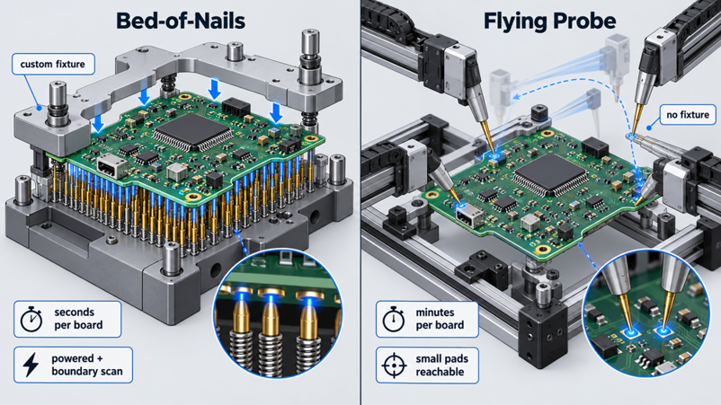
Figure 3: Bed-of-nails fixture and flying probe tester compared
| Factor | Bed-of-Nails ICT | Flying Probe | What It Means for Your Project |
|---|---|---|---|
| Tooling | Custom fixture for each design | None, programmed from CAD data | Fixture cost only pays back over volume |
| Test time per board | Seconds | Several minutes | Bed-of-nails keeps pace with a volume line |
| Set up lead time | Weeks to build and debug | Hours to program | Prototypes go to the flying probe |
| Design change | Fixture is redrilled or rebuilt | Edit the program | A fixture freezes your revision |
| Probe access | Dedicated pads on a regular grid | Smaller pads and part terminations | Dense boards stay testable |
| Powered testing | Full powered and boundary scan tests | Mostly unpowered | Bed-of-nails covers more active circuitry |
Top Advantages of In-Circuit Test for Quality Control
It has one property that makes it advantageous – it is a direct measurement of each part. It should never have to assume that the fault is with the entire board, and that saves time, less expensive repairs, and wider electrical coverage.
Rapid Defect Detection and High Accuracy
A bed-of-nails tester can perform hundreds of tests in seconds on each board. All the probes are already in place, and the tester uses relays to switch between them. Since there are no moving parts, it is feasible to test all the boards rather than sample a few.
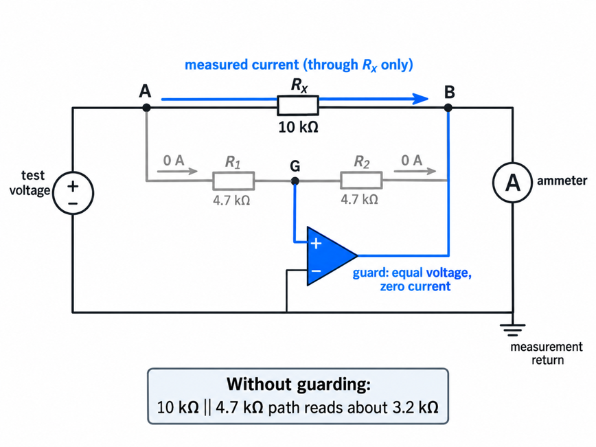
Figure 4: Guarding isolates one resistor from a parallel path
The accuracy is derived from the guarding: to check a resistor in a network, the tester sends current to one end and detects it at the other end. It maintains the middle node voltage of each parallel path at the voltage at the measuring end. Thus, the current flows in parallel into the guard, not the meter, and the meter reading is only for the target part.
Very low values require one additional step: A 10 mΩ current shunt will be smaller than the resistance of the probe and wiring in series with it, so a two-wire reading is a measurement of the fixture. The four-wire Kelvin testing technique supplies current through one pair of probes and measures voltage through another pair, thus requiring two test pads per net for such parts.
Lower Repair Costs and Higher First-Pass Yield
A defect has an increasing cost the further down the line it goes. The rule of ten is the usual estimate, and this rule proposes that the same fault will cost about ten times more at each stage. ICT detects the assembly error before it gets to the point of one joint and a soldering iron.
The majority of repair costs are for determining the problem. An unbootable board can be an hour of probing for a tech, while a ticket that says "C22 missing" is a few-minute job. The reworked board can be returned to the fixture immediately for retest, as the fault has been identified. First-pass yield is the percentage of boards that pass all tests without rework, an improvement based on feedback from ICT. If a failure occurs on board after board and the same pin fails, the issue is located upstream in a stencil aperture, a placement offset, or a reflow profile. Correcting this cause prevents the defect from accumulating.
Comprehensive Electrical Inspection
ICT checks electrical facts; that is why it detects faults that cameras can't. A camera reveals a resistor that appears to be OK, but only a measurement reveals it's 1 kΩ - the BOM calls for 10 kΩ.
| Defect | How ICT Detects It | What a Failure Usually Points To |
|---|---|---|
| Solder bridge or short | Low-voltage resistance check between nets | Excess paste or stencil misalignment |
| Open or lifted joint | Missing continuity, or a capacitive plate over the IC | Too little paste, poor coplanarity, or a cold joint |
| Wrong resistor or capacitor value | Guarded measurement against BOM tolerance | The wrong reel was loaded on a feeder |
| Missing component | Open where a value should be | Pick-up failure or a tombstoned part |
| Reversed diode or transistor | The forward voltage is read in the wrong direction | Wrong rotation in the placement program |
| Misoriented or damaged IC | Protection diode check on each pin, or boundary scan | Rotation error or ESD damage |
DFM Requirements for Successful ICT Coverage
ICT coverage is determined during layout, since the tester can only measure the net it can touch. Those three things are the location of the test points, the space around the test points, and whether the board will remain flat while under the fixture.
Strategic Test Point Placement
A test point on each net is required for full coverage; a net without a test point will not be measurable. Four-wire parts require two points per net. Several are required for the main power and ground nets to distribute the current across multiple probes, and to keep contact resistance low. Consider test points to be part of the PCB design, rather than an add-on.
A one-sided fixture is less expensive and easier to align; therefore, all test points should be on one side, usually the bottom side, of the fixture. All points on both sides are used to achieve a clamshell fixture with probes above and below. It's often worthwhile to move a couple of traces to avoid that. Even for those who design regularly, there are some common pitfalls for loss of coverage. Each of them contains a straightforward layout fix:
- The mask of a via for probing conceals its copper, so open the mask and keep the drill ≤ 0.36 mm (14 mil).
- When pressure is applied to the probe, the probe pressure can be used to close a cracked joint using the component pad as the test point; place a dedicated pad somewhere on a short trace.
- When making a test point on a power rail, multiple test points should be used to distribute the test current across them.
- Make sure there is no ink on any test pad or silkscreen that will be printed over them, and isolate the copper from the probe.
Component Clearance and Board Layout Rules
A probe tip is small; however, the barrel or receptacle is not. The clearance thus increases with component height, as probe plate relief pockets are required around tall components. Two tooling holes, which are not plated, drop over guide pins, registering each probe simultaneously. Pads close to the edge of the board are prone to landing on the seal of the fixture, so they are pushed back off the edge.
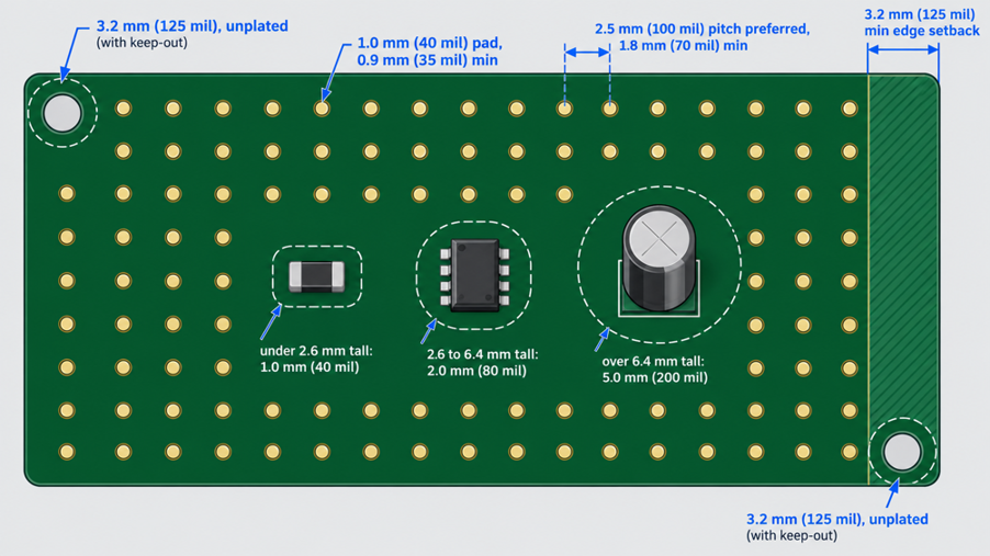
Figure 5: ICT test point size, pitch, clearance, and edge setback
| Rule | Minimum | Preferred | What It Protects |
|---|---|---|---|
| Test pad diameter | 0.9 mm (35 mil) | 1.0 mm (40 mil) | Probe lands on copper despite position tolerance |
| Test pad pitch, center to center | 1.8 mm (70 mil) | 2.5 mm (100 mil) | Allows standard 100 mil probes, the cheapest and most robust |
| Clearance to parts under 2.6 mm (102 mil) tall | 1.0 mm (40 mil) | Larger | Room for the probe barrel |
| Clearance to parts 2.6 to 6.4 mm (102 to 252 mil) tall | 2.0 mm (80 mil) | Larger | Plate material around relief pockets |
| Clearance to parts over 6.4 mm (252 mil) tall | 5.0 mm (200 mil) | Larger | Clear path past connectors and bulky parts |
| Test pad to board edge | 3.2 mm (125 mil) | 3.8 mm (150 mil) | Probes stay clear of the fixture seal |
| Tooling holes | Two, 3.2 mm (125 mil), unplated | Opposite corners with a 3.2 mm (125 mil) keep-out | Registration of the whole probe field |
Fixture Stability and Mechanical Stress Control
The pushing force on each spring probe is about 1-2N, and hundreds of spring probes are mounted on a fixture. The board is rated at 400 probes at 1.5N per probe, totaling around 600N - equivalent to the weight of a 60kg person. That load will bend the board if it is not evenly supported, and bending can cause parts to crack.
The first components to fail under flex are ceramic capacitors and BGA joints. A multiple-layer ceramic capacitor may crack internally, and this crack may not fail for weeks. BGA pads may tear the resin (under the pad), termed as pad cratering. Thus, the fixtures position their push-down fingers directly over the probe clusters, where the forces are canceled, so they do not bend the board.
Our Professional Testing Capabilities for Zero-Defect Delivery
The realistic goal is layered inspection; no single test will give a zero-defect shipment. At JLCPCB, this layering begins even on the blank board and persists throughout assembly, with each layer capturing what the others missed.
Customized ICT Fixture Design and Engineering
A custom ICT fixture designed from the same CAD information used to create the board. The probe map is drawn from the test-point coordinates; the plate is drilled to accommodate the probes; and each probe is connected to a tester channel. This implies that if a pad is revised, so is a fixture, as it's dealt with in bed-of-nails testing with high-quantity PCBs.
JLCPCB conducts electrical testing in the bare-board stage. It uses flying-probe testing for prototypes and small-volume products and bed-of-nails fixture testing for large-volume products. Assembled boards are inspected using solder paste inspection, 2D/3D AOI, X-ray inspection, flying-probe testing, and functional testing (FCT).
Multi-Stage QA: Integrating ICT with AOI and AXI
Different types of faults occur in each automated check between reflow and functional test. They are normally arranged on a typical line as follows:
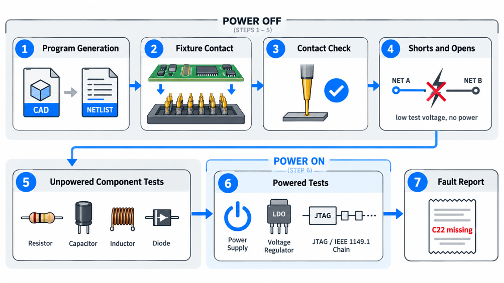
Figure 6: A multi-stage PCBA inspection line from SPI to functional test
- Because AOI (automated optical inspection) requires no contact, it is the first process performed. Cameras are used to determine the presence, position, polarity, and visible fillets, but cannot determine the presence of an invisible joint or the value of a resistor.
- AXI (automated X-ray inspection) examines BGA, QFN, and LGA bodies and inspects the underlying joints. It indicates missing balls, bridges, and voids through density, but it can't determine if a well-soldered part is the correct value.
- ICT records the electric outcome. It is a proof of the "current flows where the netlist says"; the other two questions of value remain.
JLCPCB has 2D and 3D AOI during assembly (how AOI detection works), and uses X-ray for bottom-terminated packages. If the ICT is done in those steps, the only question that remains after the functional test is whether the product works.
Strict Turnkey Manufacturing and Traceability
Turnkey means that one supplier will fabricate the board, source the parts, and assemble them. These are then all the records for one particular build, and if the value is flagged as incorrect by ICT, it is easy to identify the reel that fed it. JLCPCB provides parts from its component library; therefore, each part placed has a known part number.
Board-level traceability requires the identity to be printed on the board. JLCPCB can add a 2D barcode, a serial number, or both, with the barcode as a QR code or Data Matrix in one of three sizes: 5 × 5 mm, 8 × 8 mm, or 10 × 10 mm (197, 315, or 394 mil square). If your design already has testpoints and a clean netlist, it's ready to be built. JLCPCB allows you to upload your Gerber files to the website and instantly receive a quote for your Gerber files, assembly, and inspection.
FAQs About In-Circuit Test
Q: What is the difference between a bare-board electrical test and an in-circuit test?
Bare-board electrical test checks the empty PCB for opens and shorts against the netlist. Its requirements are set out in IPC-9252B (2016); the last revision of IPC has been published. In-circuit test runs after assembly and measures the components and joints as well. A board needs both, because a perfect bare board can still be assembled with a bridged joint.
Q: Is an in-circuit test worth it for a run of a few hundred boards?
Usually not with a dedicated fixture, because its cost is spread over too few boards, and a design change can scrap it. Flying probe testing provides much of the same unpowered coverage without tooling. A fixture pays back once the revision is stable and volume reaches thousands.
Q: Can ICT test a board after conformal coating?
Not reliably, because the coating insulates the test pads. Run ICT before coating, or mask the test pads to keep them bare.
Q: Can an ICT fixture program the microcontroller?
Yes, many fixtures program flash memory through the same probes, using the chip's programming pins as test points. That saves a separate handling step, so plan those pins on the probed side of the board.
Q: Can an in-circuit test run on a panel of boards?
Yes, a panel fixture probes every board in one press, which saves handling on small boards. Test before depaneling, but check that V-cut panelization or breakaway tabs do not flex boards that have already passed.
Conclusion
The advantages of using an in-circuit test are that it measures each part in place and it determines exactly where the fault is. It repairs quickly and allows us to address issues at the source. It is established prior to the board going to the fixture: test point on each net, clearance around high elements, and fixture designed so that probing forces never bend the board.
ICT is no longer a standalone solution, but, as boards become denser, it is used in conjunction with boundary scan and X-ray. Designs that maintain test access without incurring significant testing cost. When preparing a board for production, JLCPCB's fabrication, assembly, and inspection services allow you to produce the board with that test plan in place.

Keep Learning
PCB Testing Methods: A Comprehensive Guide to Testing and Characterizing PCBs
Key Takeaways PCB testing helps identify manufacturing defects, verify electrical connections, and ensure product quality. Different testing methods serve different purposes: AOI and X-ray detect visual and hidden defects, while Flying Probe and ICT identify electrical issues. Functional and reliability testing help evaluate circuit performance under specific operating conditions. Combining appropriate inspection and testing methods improves quality control across PCB fabrication and PCBA assembly. JL......
How PCB Thermal Cycling Tests Reveal Manufacturing Reliability
Key Takeaways Exposes Hidden Faults: Thermal expansion opens tiny cracks, catching via failures that room tests miss. Expansion Mismatch Stress: Heat differences weaken vias and solder joints over time. Standardized Testing: Follows IPC and JESD rules, failing when resistance increases. Process Prevention: High Tg materials, thick copper, and filled vias boost board life. Destructive Test: Consumes board life, so tested samples must be scrapped. A PCB thermal cycling test can detect faults that a room......
Why PCB Inspection Microscopes Matter in Electronics Manufacturing
Key Takeaways Precise Faults: ICT tests individual components to report exact pin-level failures. Layout-Driven: Coverage relies on test pad size, pitch, and component clearance. Speed vs. Tooling: Bed-of-nails tests in seconds; flying probe requires no custom fixture. Guarded Isolation: Isolates components from parallel paths to catch early defects. Layered QA: Pairs with AOI and AXI for full quality coverage. A PCB inspection microscope earns its place on a production line because the costliest defe......
How Sustainable Materials and Expert Manufacturing Ensure RoHS Compliant PCBs
Have you ever experienced that a finished shipment of products was detained at the EU customs due to a single component on the board not passing the RoHS screening? It is higher than most engineers think, and the financial blow is far bigger than the impounded goods. Wasted time, remodeling expenses, and a compliance audit that is capable of halting your whole product introduction, that is the actual cost of doing RoHS wrong. The point is as follows: RoHS-compliant PCBs cease to be a checkbox exercise......
Ensuring Superior Solderability: The Critical Role of Testing in Reliable PCB Production
Key Takeaways Core Purpose: Verifies solder wetting before assembly to prevent yield drops and joint failures. Destructive Test: Per J-STD-002, tested components and coupons cannot be reused in production. Pass Standards: Requires 95 percent solder coverage on leads and 80 percent on exposed thermal pads. Key Defects: Catches non-wetting (exposed metal), dewetting (solder pulling back), and black pad on ENIG. DFM Prevention: Use thermal relief, keep silkscreen off pads, and select the right surface fi......
Solder Joint Inspection in PCB Manufacturing : A Complete Guide to Catching Defects Early
Key Takeaways Solder Joint Inspection is critical in modern PCB manufacturing to catch defects early and ensure product reliability. By combining Solder Paste Inspection (SPI), 3D AOI for visible joints, and X-ray for hidden BGA/QFN issues, manufacturers can effectively detect common defects such as bridging, cold joints, tombstoning, and head-in-pillow. Following IPC-A-610 standards with a layered inspection strategy significantly reduces field failures while improving first-pass yield. JLCPCB’s prof......