
Flying Probe Testing: Revolutionizing PCB Quality Assurance in Modern Electronics Manufacturing
11 min
- Test Methods
- What Is Flying Probe Testing?
- Flying Probe Testing Checks for the Following
- How In-Circuit Testing Differs from Flying Probe Testing
- How Flying Probe Testing Works
- Tracks Impedance Measurement in Flying Probe Testing
- Working Principle of 4-Wire Kelvin Test
- Benefits of Flying Probe Testing
- The Disadvantages of Flying Probe Test
- FAQ about Flying Probe Testing
- Conclusion: Flying Probe Testing
The process for manufacturing printed circuit boards (PCBs) includes a critical testing phase. Each board must undergo testing to ensure manufacturers detect every electrical or circuitry problem before leaving the center. When a PCB passes this testing, it further ensures that it performs reliably. The most common types of testing methods include in-circuit testing (ICT) and flying probe testing (FPT).
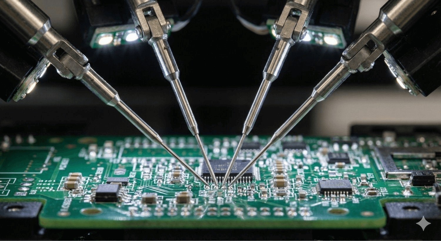
6 high-precision probes (needles), 4 on top and 2 on the bottom are programmatically able to contact component pins (including fine-pitch components) or other contact points on a printed circuit board or assembly to perform these electrical tests. In addition to an electrical test, functional tests are also possible with the Flying Probe Tester and programs can be recorded via the JTAG interface. FPT is a type of PCB test that is a highly accurate and extremely versatile technique that validates PCB assemblies without requiring fixtures or testbeds. This article provides an in-depth overview of the principles, processes, capabilities, and applications of flying probe testing for PCBs.
Test Methods
- Smart ICT: short-circuit, open-pin and component testing
- Model-Z-Impedance Test (NZT): Test out short circuits and also give characteristics of the network parameters, taking all components into account.
- Electro-scanning method: Pin connections are examined, and open solder joints are detected via the field strength.
- Optical tests: Through camera image evaluation (can be extended)
- 4 Wire Kelvin Test: Track Impedance measurement
What Is Flying Probe Testing?
Flying Probe Testing (FPT) is a type of automated testing method used for checking the electrical functionality of printed circuit boards (PCBs). It uses movable probes that "fly" across the board to make contact with various test points, measuring parameters like resistance, capacitance, and continuity. Unlike traditional in-circuit testing, which uses a fixed bed of nail fixtures, flying probe testing is flexible and doesn't require custom fixtures. Which makes it ideal for low-volume production, prototypes, and designs that frequently change.
A flying probe tester utilizes one or multiple test probes. These probes can make contact with the PCB both on top and bottom to contact test points. They then move from one place to another on the circuit board to test multiple conductors or components. They follow the instructions from a program that outlines the specific board that is being tested. These machines use highly precise needles to ensure the PCB is functioning properly and in order. FPT is also ideal for low- to mid-volume production.
Flying Probe Testing Checks for the Following
The "flying" probes are mounted on arms or heads controlled by precision robotic motion control to target test points anywhere on the PCB surface. Flying probes provide complete electrical testing coverage for assemblies ranging from simple boards up to complex multilayer PCBs with thousands of test points.
- Shorts and opens
- Pattern defects
- Voltage and frequency response
- Passive component values
- Connectivity and signal integrity
How In-Circuit Testing Differs from Flying Probe Testing
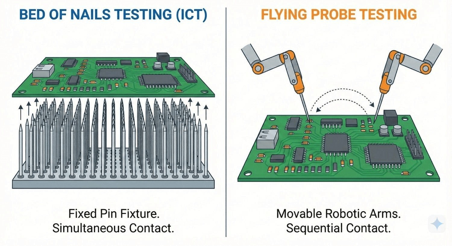
In-Circuit Testing (ICT) is a method used to assess the quality and functionality of individual components on a printed circuit board (PCB). This type of testing involves using a fixture, often called a "bed of nails". Which has numerous probes that make contact with designated test points on the PCB.
These probes inject test signals and measure electrical parameters like voltage, current, resistance, and capacitance to verify that components are correctly placed, functioning properly, and soldered without defects. ICT is particularly effective for mass production but requires a custom test fixture, which can be costly and time-consuming to create, making it less suitable for prototypes or low-volume runs.
How Flying Probe Testing Works
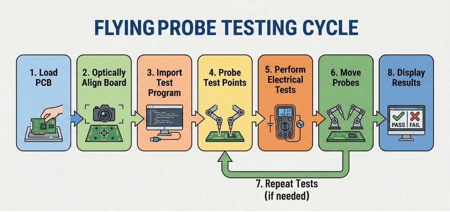
-
Load PCB
The PCB is loaded into the test system on precision fixtures.
-
Optically Align Board
Optical cameras align the PCB coordinate system to the tester.
-
Import Test Program
Test parameters are imported from CAD data.
-
Probe Test Points
Probes on multiple heads touch down on defined test nodes.
-
Perform Electrical Tests
The tester stimulates and measures based on programmed tests.
-
Move Probes
Heads reposition probes to cover all definable nodes.
-
Repeat Tests
Steps 4-6 are repeated until all points are verified.
-
Display Results
Pass/fail reports clearly identify defects for repair.
All these points can be collectively understood by three steps given below:
Step 1: Programming and Generation of Test Bench
Before you can begin, you must create a flying probe testing test program. Test programs are usually developed on an offline PC using a test program-generating application. These applications typically require Gerbers, Bill of Materials (BOM), and Electrical computer-aided design (ECAD) files to generate test points.
Step 2: Sample Loading Process
Once you have created the test program, it is time to load it onto the conveyor belt inside of the tester. The board travels on the conveyor belt to the testing area where the probes operate. The circuit board may be solo or there may be several boards and testing will depend on the program controls.
Step 3: Testing Process
Probes can then "fly" around the circuit board following the test program. They use test signals to conduct electrical and functional tests on various points of the board. The measurements will be further processed to determine whether a particular circuit portion meets expectations.
If the board fails to meet the expected results or deviates from the set program, the probes will signal that the unit has a defect and, therefore, failed the test.
Tracks Impedance Measurement in Flying Probe Testing
4-wire Kelvin testing, also known as 4-wire resistance measurement or 4-point probe measurement, is a technique used to accurately measure low resistance values. It is commonly used in applications where high precision and low measurement error are required, such as in the testing of electrical conductors, resistors, or semiconductor devices. Here in the PCB design, resistance from one to another point is measured by using this method.
Working Principle of 4-Wire Kelvin Test
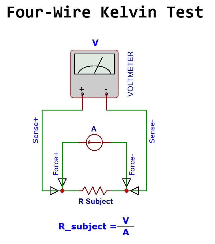
1Current-Carrying Probes
The two current-carrying probes are connected to the ends of the component or material being tested. These probes are responsible for passing a known and precise amount of current through the test sample. Usually, these are known as outer probes.
2Voltage-Sensing Probes
The two voltage-sensing probes are positioned on the test sample, usually at a specific distance from the current-carrying probes. These probes measure the voltage drop across the test sample accurately. These probes are known as internal probes.
3Measurement Process
During the measurement, a constant current is passed through the test sample using the current-carrying probes. The voltage drop across the sample is then measured using the voltage-sensing probes. Since the current-carrying and voltage-sensing probes are physically separated, the voltage measurement is not affected by the resistances of the connecting wires or contact resistances. There will be no voltage drop across the contact pins of the voltmeter because of its high internal input impedance. This arrangement allows for a more accurate determination of the sample's resistance.
4Calculation
The resistance of the test sample is calculated using Ohm's law (R = V/I), where R is the resistance, V is the voltage measured across the sample, and I is the current passing through the sample. This method is particularly useful when measuring low resistances or when high measurement accuracy is required.
Benefits of Flying Probe Testing
There are many advantages to utilizing FPT. The following are some of the greatest benefits of incorporating flying probe testing in printed circuit board assembly processes:
Pros
- Lower testing costs: FPT has lower costs compared to ICT because it does not require custom fixtures.
- Ideal for small to medium-scale production: Flying probe testing is well-suited for small-batch production due to its low development costs and short development time. While it may not be suitable for mass production, it can still be used for samples and prototypes.
- Shorter development time: The runtime of FPT varies depending on the size of the PCB. In most cases, the testing time per board is approximately 5 to 15 minutes.
- Greater flexibility: The automation of FPT enhances flexibility in making test changes. While there are limitations for some more complex tests, the ability to handle variations makes this approach useful.
- Accuracy and precision: The positioning of the testing probes has high accuracy and reliability, helping prevent issues in the finished products.
The Disadvantages of Flying Probe Test
Cons
- Potential for physical damage: Since flying probes make direct physical contact with vias and test pads and tend to create small dimples on the board surface, some OEMs consider this a manufacturing defect. However, with the continuous advancement of science and technology, this problem will be solved by the appearance of upgraded flying probe testers.
- Potential for poor soldering: Sometimes, when a flying probe tester is working on a component that does not have a test pad, it is possible for the probe to come into contact with the component lead, resulting in loose leads or poor soldering.
- Not suitable for high-volume and large complex circuit boards: FPT only has a small number of test probes working, and they must cover all test points on the circuit board. For smaller boards and samples, this is usually not a problem, but for large, complex boards produced in high volumes, it is not advisable.
Despite the above disadvantages, FPT is still regarded as an important testing method in PCB manufacturing and PCB assembly, and will always play a vital role in leading electronic products to achieve superior performance and high reliability.
Further reading: PCBA Testing Guide: Methods, Processes, and Quality Standards
FAQ about Flying Probe Testing
Q: At what production volume should I switch from Flying Probe to In-Circuit Testing (ICT)?
The industry "break-even" point is typically between 50 and 250 boards. For quantities below this, FPT is more cost-effective because you save the $2,000–$6,000 cost of building an ICT fixture. However, once production exceeds ~250 units, the slow cycle time of FPT (15 mins/board) becomes a bottleneck, making the instant testing of ICT (<1 min/board) the cheaper and faster option despite the initial fixture cost.
Q: Can Flying Probe Testing check components hidden under BGAs (Ball Grid Arrays)?
Generally, no. FPT requires physical access to a test point. If a BGA's solder joints are hidden beneath the package and are not "fanned out" to an accessible via or test pad, the probe cannot touch them. However, advanced FPT machines use capacitive "TestJet" sensors to detect open circuits on BGA pins without needing direct physical contact.
Q: What if I don't have the CAD data? Can I still do Flying Probe Testing?
It is possible, though not easy. This method is referred to as "Reverse Engineering" or "Learning from a Golden Board". The machine contains a physically scanned good board and is therefore able to learn all the points' impedances and create the test program according to that reference. The process is less precise than using original CAD/Gerber data and takes much more time to set up, but it is definitely worth it for old boards where data has become unavailable or been lost.
Q: Does the "dimple" left by the probe affect the reliability of the PCB?
In the vast majority of cases, no. The small indentation left by a probe on a solder joint is usually cosmetic and falls within acceptable IPC manufacturing standards. However, if a probe accidentally hits a bare copper track or the body of a small resistor, it can cause damage. To prevent this, engineers utilize "soft landing" programmable speed/pressure settings and restrict probing to solid test pads or solder joints only.
Conclusion: Flying Probe Testing
In summary, flying probe testing delivers fast, accurate, and comprehensive verification of PCB assembly quality while minimizing the need for custom fixtures. The techniques enabled by advanced robotic motion control, probe technologies, and automation capabilities allow flying probe testers to inspect the vast majority of assembled boards delivered from fabrication and assembly houses. By offloading tedious manual testing, flying probes scale provides quality and reliability assurance in an efficient and cost-effective manner. With continual advances expanding their scope, flying probe testing solutions will take on an increasingly pivotal role in electronics manufacturing.
Popular Articles
• PCB X-Ray Inspection Explained: Non-Destructive Testing for PCB Assembly Quality Control
• Flying Probe Testing: Revolutionizing PCB Quality Assurance in Modern Electronics Manufacturing
• Solder Paste Inspection (SPI): A Complete Guide to Process Control in SMT Assembly
• What Is PCBA Testing? Complete Guide to Inspection Methods, Process, and Quality Control
• Automated Optical Inspection (AOI): Principles, Defects, and PCB Applications
Keep Learning
PCB X-Ray Inspection Explained: Non-Destructive Testing for PCB Assembly Quality Control
In the era of miniaturization, modern printed circuit boards (PCBs) face an invisible challenge: verifying the quality of solder joints hidden beneath components. With Ball Grid Array (BGA) packages featuring pitch sizes down to 0.3mm and Quad Flat No-lead (QFN) components concealing critical thermal connections, traditional optical methods are blind to the most critical failure points. PCB X-ray inspection has emerged as the definitive solution. This guide explores the technical foundations, applicat......
Flying Probe Testing: Revolutionizing PCB Quality Assurance in Modern Electronics Manufacturing
The process for manufacturing printed circuit boards (PCBs) includes a critical testing phase. Each board must undergo testing to ensure manufacturers detect every electrical or circuitry problem before leaving the center. When a PCB passes this testing, it further ensures that it performs reliably. The most common types of testing methods include in-circuit testing (ICT) and flying probe testing (FPT). 6 high-precision probes (needles), 4 on top and 2 on the bottom are programmatically able to contac......
Transistor Pin Identification Using a Multimeter: Complete Step-by-Step Guide
Identifying transistor pins correctly is one of the first checks every engineer, hobbyist, and EE student needs before placing a bipolar junction transistor (BJT) into a circuit. A wrong base, collector, or emitter assignment can destroy the part on first power-up or leave a prototype board silently non-functional. This guide explains how to identify transistor pins using a multimeter when no datasheet is available. The method works because a BJT is internally built from two PN junctions sharing a com......
Solder Paste Inspection (SPI): A Complete Guide to Process Control in SMT Assembly
In today's Surface Mount Technology (SMT) manufacturing world, the consistency of the solder paste deposit is the element that drives electrical performance, mechanical shear strength, and long-term reliability of assembled Printed Circuit Boards. The solder paste is the medium that bonds the component terminations to the copper pads on the PCB. Therefore, any variations in the solder paste deposit in terms of volume, thickness, or placement will drastically impact the quality of the solder joints in ......
What Is PCBA Testing? Complete Guide to Inspection Methods, Process, and Quality Control
In modern electronics, the performance and long-term reliability of a finished product are directly tied to its Printed Circuit Board Assembly (PCBA) quality control. Even small defects at the board level—such as microscopic solder cracks, misaligned components, or incorrect passive values—can cascade into costly field failures, product recalls, and long-term damage to a brand's reputation. High-quality PCBA is not achieved through a single final inspection; it is the result of a repetitive and system......
Automated Optical Inspection (AOI): Principles, Defects, and PCB Applications
What Is Automated Optical Inspection (AOI)? Automated Optical Inspection (AOI) is a machine-based inspection method that uses high-resolution cameras, controlled lighting, and image-processing software to automatically detect visual defects on printed circuit boards (PCBs). It is widely used in PCB fabrication and PCB assembly to inspect components, solder joints, and conductor patterns without physical contact. By comparing captured images with design data or reference models, AOI systems can quickly......