
PCB Cleanliness in Professional Manufacturing : Preventing Contamination and Ensuring Long-Term Reliability
11 min
- Integrated Cleanliness Control in Modern PCB Fabrication
- Industrial-Grade Cleaning Methods for High-Reliability Assemblies
- How Professional Manufacturing Minimizes the Need for Post-Process Cleaning
- Best Practices for Long-Term PCB and PCBA Reliability
- Frequently Asked Questions (FAQ)
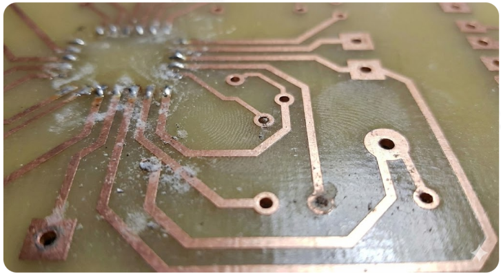
In the construction of PCBs, the boards are contaminated with all sorts of dirt at almost every stage. In the soldering process, the flux (either rosin-based or more recent organic forms) may cause residues or ionic salts to remain on the pads and traces and be sticky. Next there is etching, plating and micro-etching; the chemical processes will put metal ions on the copper unless the rinsing is complete. Tiny particles of metal shavings, fiberglass dust, and laminate fragments are also thrown out in drilling, routing, and depaneling.
Such bits may lodge between parts, creep into vias or lodge between closely spaced conductors. In a non-regulated setting, such air pollutants as lint and common dust just increase the danger. The mess is augmented by human and mechanical handling. Fingerprints carry oils and salts and machines at factories can also deposit a thin layer of lubricant that attracts moisture. Studies in the industry continually indicate that PCBs are subjected to various contamination causes throughout the fabrication process and even the smallest traces may end up being points of failure.
Typical contaminant categories include:
- Flux activators and halides
- Metal particles
- Dust, fibers, and laminate debris
- Residual cleaning solvents
- Trapped moisture and humidity
Impact of Residues on Electrical Performance and Long-Term Reliability
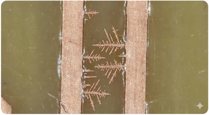
I, as a PCB enthusiast who is building PCBs, am learning that residual residues actually slow down the performance of the boards. Any splatter of dust or solder may block the airflow and cause hot spots. The dust can form a thin layer, which will serve as an insulator, disturbing the heat dissipation. Flux residues are particularly worrying since most of them absorb water, when this occurs, they form conductive films which reduce Surface Insulation Resistance (SIR). These films can also induce electrochemical migration with an electrical bias, in which the metal ions are dissolved and redeposited as dendrites that bridge the conductors. Flux or cleaning agent ionic residues, salts and amines also reduce SIR and hasten corrosion. In essence, ionic contamination results in solution conductivity, which provides an environment in which corrosion and dendrite growth occur, which eventually leads to the failure of the board.
Electrical and functional consequences include:
- Increased trace and joint resistance due to oxidation
- Leakage currents and electrical noise
- Intermittent or permanent shorts from dendritic growth
- Increased sensitivity to humidity and voltage stress
Why Uncontrolled Contamination Leads to Field Failures
In critical electronics like aerospace and medical, even a minute contamination can cause costly field failures. For example, a single incompletely cleaned solder joint in an aircraft control PCB could cause a short under vibration.
Industry failure analyses indicate that nearly one-third of high-reliability PCB failures are due to contamination. While consumer devices may tolerate minor defects, mission-critical electronics cannot. For professional manufacturers, cleanliness is therefore treated as a core reliability requirement.
Integrated Cleanliness Control in Modern PCB Fabrication
Automated Cleaning Steps in Professional Manufacturing Lines
Today’s PCB fabs build cleaning into the process at multiple points. After photoresist patterning and UV exposure, boards are typically washed with an alkaline solution to strip off undeveloped resist. Similarly, before electroplating holes and traces, the bare board is cleaned thoroughly to ensure the new copper bonds correctly. These cleaning steps are automated by computer-controlled spray to remove resist, etch residues, oxides and oils at each stage. Manufacturers like JLCPCB document such steps explicitly. Automated inline washers may also be interspersed after drilling or just before assembly to sweep away any debris. The key is that professional lines use controlled machines and chemistry (rather than a manual swipe) to rinse and dry PCBs at each fabrication step.
No-Clean and Low-Residue Flux Strategies in Controlled Processes
To minimize cleaning needs, factories often use no-clean or low-residue flux. No-clean fluxes are formulated to leave behind inert, non-conductive residues that theoretically do not require washing. Water-soluble fluxes that are readily rinsed with deionized water are reserved for high-activity needs or very dense BGAs.
However, even no-clean processes are carefully controlled. The flux choice is matched to the profile so that decomposition is complete during reflow. Assembly engineers also optimize solder paste volume and stencil design to minimize excess flux. In aerospace or medical device manufacturers may still perform a final cleaning. As one soldering guide explains, in critical assemblies, any remaining flux film can attract moisture or degrade under thermal cycling, so manufacturers consider cleaning residues in certain cases even with no-clean flux.
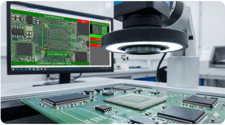
In-Line Inspection and Ionic Contamination Testing Standards
Modern fabs don’t rely on look and hope. They apply IPC and military cleanliness standards as quality gates. Inline automated optical inspection (AOI) cameras routinely scan boards for visible residues, missing chips, or unclean pads. Electrical tests help catch any leakage caused by conductive residues. For ionic cleanliness, standard tests exist for the IPC-TM-650 method or surface insulation resistance (SIR) measurements quantify board conductivity.
Typical acceptance limits range from 0.1 to 1.0 µg NaCl-equivalent/cm², depending on product class and application. These objective metrics ensure contamination remains within safe limits before boards are released.
Industrial-Grade Cleaning Methods for High-Reliability Assemblies
Ultrasonic and Aqueous Cleaning in Volume Production
For high-volume runs, factories often employ industrial cleaning machines. Ultrasonic immersion is common for boards are placed in a tank of cleaning solution. High-frequency sound waves create cavitation bubbles that scrub beneath and between components. This can remove stubborn flux under BGAs or in hidden solder joints.
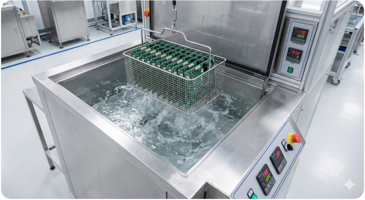
Boards are conveyed through a series of wash and rinse tanks. Often brushes or spray nozzles are used and then dried with jets of hot air or vacuum dryers. Aerospace industry sources note that batch aqueous systems are efficient for large PCB lots. These systems are flashpoint-free and reuse water with filtration. According to cleaning experts, the aqueous approach is environmentally friendly and thorough, though it does require wastewater treatment.
Vapor Degreasing and Precision Solvent Applications
Where water is not a good choice, or a super fine cleaning is required, vapor degreasers or solvent-based processes are considered. Vapor degreasing uses a low-surface-tension solvent that is heated in vapor; the vapor condenses on the cooler PCB, dissolving oils and organics, and drips off. The board is clean, dry and spotless. It is particularly widely used with tight-pitch parts since the low-viscosity vapor can be used to move under chips and connectors to dissolve the residues. Contemporary degreasers are even more efficient - they can recycle the solvent over many hours, hence efficient on large runs.
Most manufacturers clean individual assemblies manually or with precision, typically by use of electronics-grade solvents such as isopropanol, specialized flux removers or minimal-residue defluxers. Such precision products must not be conductive and evaporate fast, hence you do not end up with a residue.
Specialized Techniques for Conformal Coating Preparation
A second cleaning step is important before the application of protective conformal coatings. Different techniques such as plasma cleaning, subject the board to ionized oxygen, which removes microscopic organic compounds and prepares the surface. This dry process has the capability to clean to nanometer-thickness films, and is therefore critical when it comes to medical-device PCBs, where cleanliness is vital.
How Professional Manufacturing Minimizes the Need for Post-Process Cleaning
DFM Guidelines That Prevent Contamination from the Design Stage
Design-for-Manufacturing (DFM) plays a key role in cleanliness. Good DFM ensures that boards are easy to clean and inspect. For example, placing test coupons and fiducials allows AOI machines to work without obstruction. Spacing between components is planned so that cleaning sprays can reach underneath. Designers may choose removable standoffs or coverlays in areas where cleaning jets must reach, and they may minimize unnecessary through-hole joints. Even solder mask and silkscreen are selected to resist solvents.
While not often written down in standards, these practices are common. DFM guidelines that emphasize clear paths for cleaning fluids and avoid hidden crevices lead to cleaner boards with less rework
Benefits of Cleanroom Assembly and Controlled Environments
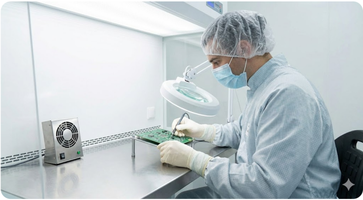
The assembly environment itself is tightly controlled. High-reliability PCBs are assembled in cleanrooms, where air filters remove dust and personnel wear gloves and smocks to avoid skin oils contaminating boards. Workstations are ESD-safe with ionizing blowers that neutralize static-charged particles. Temperature and humidity are kept in narrow bands – too much humidity invites corrosion, too little can create static. Component storage is also contain humidity Indicator Cards and dry cabinets keep boards and parts moisture-free.
Best Practices for Long-Term PCB and PCBA Reliability
Preventive Handling and Storage in Professional Workflows
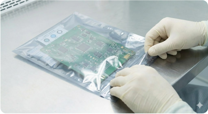
Once all is made it is necessary to maintain everything clean as well. The PCBs and kits are normally stored in anti-static, moisture-sealed bags. You will also find humidity desiccants or dry boxes which are closed to prevent the intrusion of humidity. As the individuals are working with the boards they usually put on finger cots or gloves to ensure that they do not smear the bare copper with skin oil. Kitting areas employ lint-free mats and they continue wiping down all things. Lastly, the completed boards are UV inspected and even an IR hotspot scan is performed, and then they get to the shipper.
It is very important to discuss component moisture- MSL. The fabs with the highest technology monitor the floor-life of reels and bake any parts that have exceeded their dry time. That prevents other defects lurking in the background such as solder splatter or package cracking that might appear to be contamination issues. In the production process, boards could be dried with a vacuum following a wet clean, and occasionally they can be coated with a thin anti-tarnish film should they be stored a long time.
Partnering with Manufacturers for Built-In Cleanliness Assurance

For designers and engineers, the best way to ensure PCB cleanliness is to work with a capable manufacturer. Ask your fab or PCBA service about their cleanliness controls: Do they follow IPC Class 3 guidelines? What is their post-assembly wash process? Can they provide rosette (ionic test) reports or SIR data? A top-tier EMS provider like JLCPCB, for example, integrates rigorous, technology-driven inspection throughout the entire assembly process. They often hold certification (UL/ISO/IPC standards) that include cleanliness criteria.

Frequently Asked Questions (FAQ)
Q. How does PCB contamination affect surface insulation resistance (SIR)?
Contamination, especially ionic residues from flux or cleaning agents, reduces surface insulation resistance by forming conductive films on the PCB surface. Under humidity and electrical bias, these films enable leakage currents and electrochemical migration.
Q. Is visual inspection enough to verify PCB cleanliness?
No. Many ionic contaminants are not optically visible. While Automated Optical Inspection (AOI) can detect visible residues or solder defects, quantitative methods such as ROSE testing, SIR testing, or ion chromatography are required to accurately assess ionic cleanliness.
Q. Why do “no-clean” assemblies sometimes still fail in the field?
No-clean fluxes leave low, non-conductive residues only when process conditions are tightly controlled. Improper reflow profiles, excess solder paste, or harsh operating environments can cause these residues to absorb moisture or degrade over time, leading to leakage currents or corrosion.
Q. How does contamination impact high-voltage or high-impedance circuits?
In high-voltage or high-impedance designs, even extremely small leakage paths can distort signals, increase noise, or trigger breakdown events. Contamination reduces creepage and clearance effectiveness, increasing the risk of arcing and insulation failure.
Can contamination be trapped permanently inside the PCB?
Yes. Contaminants can become trapped inside vias, under bottom-terminated components (BTCs), or between internal layers if cleaning is insufficient. Once sealed, these residues are difficult or impossible to remove and can lead to long-term reliability issues.
Q. Is post-assembly cleaning always required?
Not always. Many consumer and industrial products use controlled no-clean processes without post-assembly washing. However, high-reliability, harsh-environment, or long-lifecycle products often require additional cleaning and verification to meet stringent ionic cleanliness limits.
Q. Can contamination affect thermal performance even if the circuit works?
Yes. Dust layers, flux films, or residues under components act as thermal insulators. Even if the circuit functions electrically, elevated temperatures can accelerate aging, reduce component lifespan, and increase failure rates.
Keep Learning
Solder Joint Inspection in PCB Manufacturing : A Complete Guide to Catching Defects Early
Key Takeaways Solder Joint Inspection is critical in modern PCB manufacturing to catch defects early and ensure product reliability. By combining Solder Paste Inspection (SPI), 3D AOI for visible joints, and X-ray for hidden BGA/QFN issues, manufacturers can effectively detect common defects such as bridging, cold joints, tombstoning, and head-in-pillow. Following IPC-A-610 standards with a layered inspection strategy significantly reduces field failures while improving first-pass yield. JLCPCB’s prof......
3D AOI Inspection Explained : How It Catches Defects That 2D Systems Miss
Key Takeaways 3D AOI Inspection has become essential in modern PCB assembly by using advanced height and volume measurement to detect critical solder defects that traditional 2D AOI systems routinely miss, such as lifted leads, insufficient solder, head-in-pillow, and component coplanarity issues. By delivering precise 3D data through structured light or Moire technology, it significantly reduces false calls, improves first-pass yield, and ensures long-term reliability according to IPC-A-610 standards......
How Sustainable Materials and Expert Manufacturing Ensure RoHS Compliant PCBs
Have you ever experienced that a finished shipment of products was detained at the EU customs due to a single component on the board not passing the RoHS screening? It is higher than most engineers think, and the financial blow is far bigger than the impounded goods. Wasted time, remodeling expenses, and a compliance audit that is capable of halting your whole product introduction, that is the actual cost of doing RoHS wrong. The point is as follows: RoHS-compliant PCBs cease to be a checkbox exercise......
Preventing PCB Warping: Best Practices for Design and Manufacturing
In the design and manufacturing process of electronic equipment, PCB (Printed Circuit Board) warpage is a common but troublesome problem. PCB warping not only affects the performance and reliability of the device but can also cause connectivity issues and other serious consequences. Therefore, it is crucial to understand how to prevent and resolve PCB warping. This article will explore some best practices in design and manufacturing to help you effectively prevent PCB warpage problems from occurring. ......
PCB Cleanliness in Professional Manufacturing : Preventing Contamination and Ensuring Long-Term Reliability
In the construction of PCBs, the boards are contaminated with all sorts of dirt at almost every stage. In the soldering process, the flux (either rosin-based or more recent organic forms) may cause residues or ionic salts to remain on the pads and traces and be sticky. Next there is etching, plating and micro-etching; the chemical processes will put metal ions on the copper unless the rinsing is complete. Tiny particles of metal shavings, fiberglass dust, and laminate fragments are also thrown out in ......
PCB Basics 5: PCB Testing and Quality Assurance
Welcome to the realm of PCB testing and quality assurance! Quality control is always a crucial part of different industries. Great quality control not only could generate more energy for customers’ electronic projects, but it could also embark on certification and guarantee to the electronic industry. Let’s learn the importance of testing and quality assurance in PCB manufacturing. The Significance of Testing and Quality Assurance in PCB Manufacturing: Testing and quality assurance are extremely impor......