EasyEDA Pro vs KiCad: GPT-6 Astra PCB Design Compared
15 min
- EasyEDA Pro vs KiCad at a Glance
- The Same Amplifier in Both EasyEDA Pro and KiCad Projects
- How GPT-6 Astra Built Each Project
- Ground Copper Editing in EasyEDA Pro vs KiCad
- Footprints and Component Links in EasyEDA Pro vs KiCad
- Comparing the EasyEDA Pro and KiCad Check Reports
- Libraries, Portability, and Automation: EasyEDA Pro vs KiCad
- Manufacturing Files and Component Sourcing in EasyEDA Pro vs KiCad
- Prompts That Improve AI-Generated PCB Projects
- Conclusion
- FAQs
Key Takeaways
- What is being compared: Two versions of the same TPA3116D2 stereo amplifier project, each created by GPT-6 Astra in a different EDA tool. The comparison focuses on what you can actually do with the delivered project afterward.
- Ground copper: In the EasyEDA Pro project, the ground copper is stored as 28 fixed filled regions. In KiCad, it remains as two native copper zones that can automatically refill after layout changes.
- Verification: KiCad initially reported 46 schematic-parity issues. These were resolved by correcting component fields and no-connect definitions, without adding extra rule exclusions.
- What neither project proves: Both projects passed their configured software checks, but neither board has been fabricated, assembled, electrically tested, or reviewed through a formal DFM process.
Comparing EasyEDA Pro and KiCad becomes a different question when an AI agent is building the project for you. At that point, the comparison is not only about which tool has the better editor, router, or interface. It is also about the quality of the project the agent leaves behind.
The schematic may be correct, the board may be routed, and the design checks may pass. Yet, the next edit can expose problems with footprint libraries, component links, copper zones, or project portability.
To examine that difference, GPT-6 Astra was used to produce the same TPA3116D2 stereo amplifier twice. One version was created as a native EasyEDA Pro project, while the other was built as a native KiCad project.
The goal is not to declare one EDA platform better than the other. Instead, the comparison looks at what happens after the AI-generated project is handed back to the engineer.
In this guide, you will learn:
- What each delivered project actually contains and what still needs manual attention.
- How EasyEDA Pro and KiCad handle ground copper, footprint identity, and schematic-to-PCB links.
- What their ERC, DRC, and project-check reports can confirm.
- Which requirements should be included in an AI PCB design prompt to ensure the final deliverable remains editable, portable, and easy to revise?
EasyEDA Pro vs KiCad at a Glance
For future revisions, I would open the KiCad project first because its schematic, libraries, and copper remain native and editable. EasyEDA Pro is still practical if you already prefer its editor and integrated ordering workflow.
| Decision | EasyEDA Pro project | KiCad project |
|---|---|---|
| What was delivered | Native Pro project holding the schematic, PCB, and embedded libraries | Native project with two linked schematic sheets, PCB, and local libraries |
| Ground copper | 28 fixed filled regions | Two native refillable GND zones |
| Schematic-to-board link | Associations rebuilt with unique footprint names and identifiers | Schematic UUID paths linking all 45 footprints |
| Verification recorded here | Native DRC plus an independent check of the saved project | Native ERC, DRC, schematic parity, and a portability recheck |
| Sourcing workflow | Integrated parts-selection and PCB-order tools | Exported files for the selected fabricator and assembler |
| Work before the next revision | Regenerate or replace the imported ground regions | Edit, refill the zones, and rerun the checks |
The sourcing and local-file rows are based on the EasyEDA Pro parts-selection guide and the KiCad project manual. The copper and verification rows apply only to these two delivered projects.
What This EasyEDA Pro vs KiCad Comparison Cannot Tell You
EasyEDA Pro used roughly 1.5× as many tokens as the KiCad project. Four limits, therefore, apply to the comparison below:
- No layout-quality claim: Both projects carry the same circuit, so neither demonstrates better placement or routing.
- No hardware claim: Neither board has been fabricated, assembled, or measured.
- No manufacturability claim: No DFM upload, factory review, quotation, or order took place.
What they do support is a comparison of the delivered files. That question is narrower than which tool is better, but it is the one you actually face.
Before moving to hardware validation, check your components in the JLCPCB Parts Library and verify that the required parts are available for your design.
- Then upload your PCB files to get a quote for PCB fabrication and assembly.
The Same Amplifier in Both EasyEDA Pro and KiCad Projects
Both deliverables use the same stereo Class-D amplifier because the brief for them was identical. It asked for a single 12 V supply, stereo input and output, 4 Ω per channel, SMD parts, and a small board.
Using the same circuit makes the file comparison fair, because the differences below do not come from different amplifier designs. The physical result is the same in both projects:
- Device: TPA3116D2DADR in the top-PowerPAD package, with the exposed thermal pad on top for heatsink attachment.
- Board: 44 × 34 mm, two copper layers, 1.6 mm FR-4, and 1 oz copper.
- Assembly: 40 fitted SMD components, all placed on the top side.
- Instances: 45 footprint instances and 120 SMD pads. J1 to J4 and TP1 are wire-and-test pads rather than purchased connectors.
- Interconnect: 51 plated vias with a 0.30 mm drill and 0.60 mm diameter. There are no unplated or mounting holes.
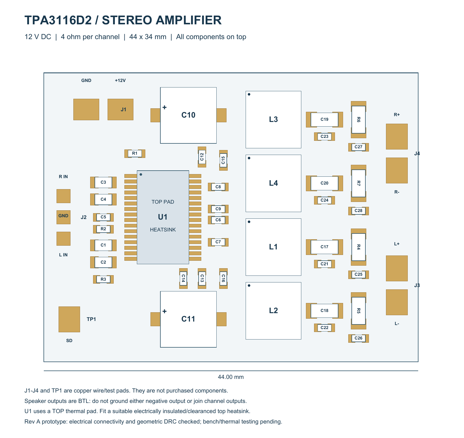
Figure: Exported assembly map of the 44 × 34 mm amplifier
Those dimensions are specific to these two projects, not a minimum for the circuit. Adding terminal blocks, mounting holes, or a larger heatsink would increase the board size in either editor.
How GPT-6 Astra Built Each Project
Each project used a desktop agent environment with file access, application control, and locally installed EDA software. A browser chat window cannot reproduce that setup, because none of those interfaces reach it.
The environment used EasyEDA Pro 3.2.149 in Half Offline mode, KiCad 10.0.4, and Freerouting 2.0.1. OpenAI documents the model's coding and computer-use behavior. No plugin, API, or partnership with KiCad, EasyEDA, or JLCPCB was involved, because the model operates each existing interface.
1. The EasyEDA Pro Project
The initial request asked whether the model could drive the already-open EasyEDA Pro window. Work then ran through the native editor and its import path, so each stage happened inside Pro:
- Circuit: The schematic was drawn as native EasyEDA Pro objects and tied to named nets.
- Libraries: Component definitions were embedded in the project rather than left as external references.
- Board: A paired schematic and PCB archive was imported, then synchronized inside Pro.
- Correction: Footprint associations were rebuilt after the initial import showed mismatches.
- Checks: The final project was verified with the native DRC and an independent check of the saved files.
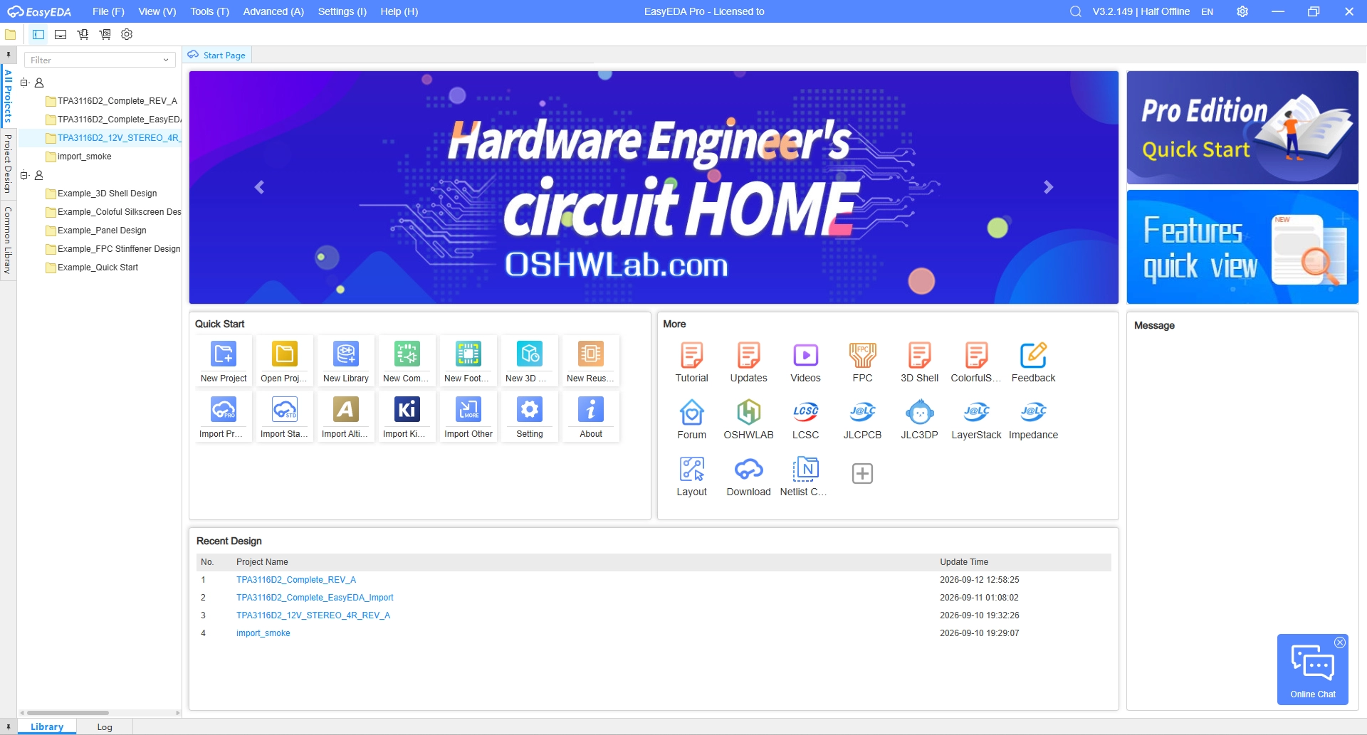
Figure: EasyEDA Pro 3.2.149 in Half Offline mode
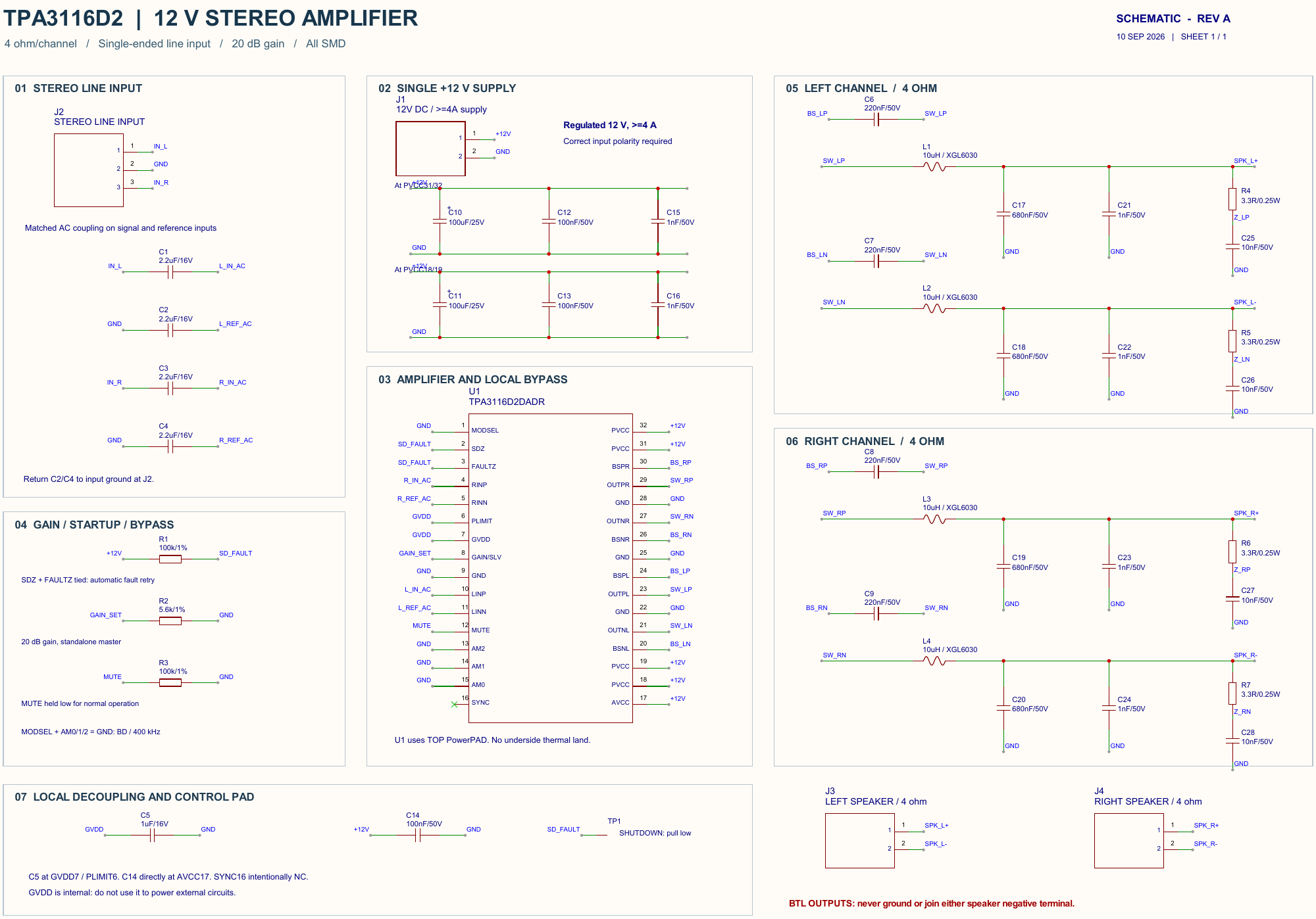
Figure: The native EasyEDA Pro schematic
2. The Native KiCad Project
The KiCad version was requested as a native project, not exported artwork, so the schematic had to remain fully editable as KiCad objects. Five results came from that run:
- Two linked sheets: A root schematic and Output_Filters.kicad_sch, which contains the bootstrap capacitors, LC output stages, and speaker pads.
- Local libraries: TPA3116_Native.kicad_sym and TPA3116_SMD.pretty, referenced through project tables using ${KIPRJMOD}.
- Component links: Schematic UUID paths link all 45 footprints, while 40 fitted components include project-relative 3D model links.
- Synchronized data: Component values, voltage ratings, manufacturer fields, and intentional no-connects are kept consistent.
- Native outputs: ERC and DRC reports, fabrication files, and CAD plots were generated from the checked project.
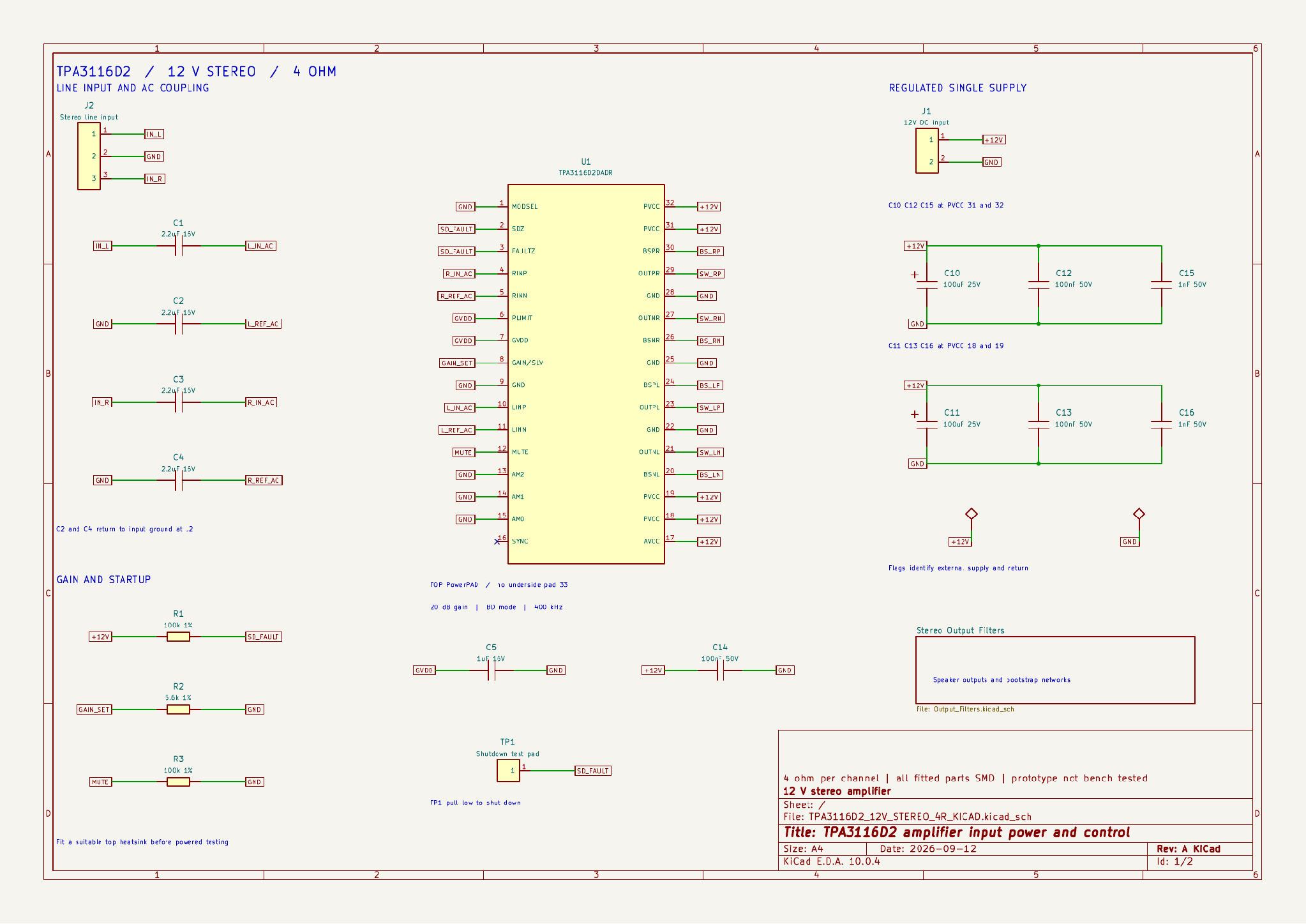
Figure: The root KiCad schematic sheet exported from the native project
This page compares the two results, neither run is repeated in full here. The native KiCad project and the EasyEDA Pro project each have their own record.
How the Copper Was Routed in Both Projects
Neither board was routed entirely by hand nor entirely by an autorouter, so the disclosure belongs before any copper claim. The critical supply, bootstrap, and switching copper were defined and locked first.
A local Freerouting 2.0.1 run then completed the remaining low-current nets. Once it finished, the locked copper was confirmed intact, the zones were refilled, and the same sequence was applied in both projects.
Ground Copper Editing in EasyEDA Pro vs KiCad
The largest practical difference between the deliverables lies in the ground copper. One project stores it as fixed regions describing a finished layout, while the other stores zones that regenerate after a change.
Fixed Filled Regions in the EasyEDA Pro Project
Ground copper was added to the EasyEDA Pro project with 28 fixed filled regions. Those regions preserve the clearance openings from the original layout, so moving a component does not automatically rebuild the copper around its new pad position.
There are two ways to handle later edits:
- Regenerate: Rebuild the imported copper regions after the change, then rerun the native DRC.
- Replace: Convert the fixed regions into native EasyEDA Pro copper areas, then rebuild and check the board.
This limitation comes from the conversion path used for this project, not from EasyEDA Pro itself. The editor supports native copper areas that can be rebuilt after layout changes.
Editable Copper Zones in the KiCad Project
The KiCad project keeps two native GND zones, one on each copper layer, with their outlines, net assignments, and fill settings intact. After moving a component, refilling the zones automatically recalculates the required clearances.
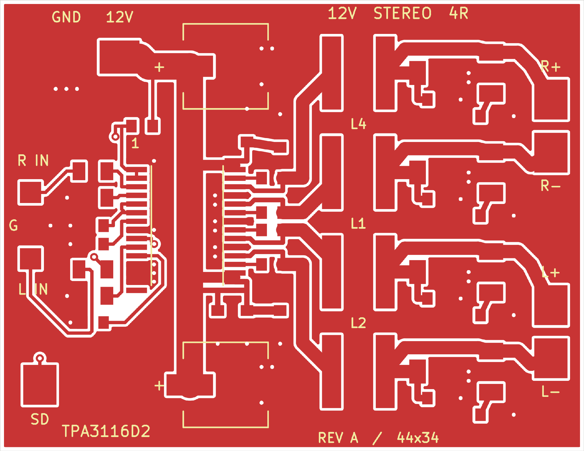
Figure: The KiCad front copper plot exported from the native board
Refilling the zones does not repair broken tracks or longer return paths, so ERC, DRC, and parity checks still need to be rerun after the edit. Those controls are documented in the KiCad 10 manual.
Footprints and Component Links in EasyEDA Pro vs KiCad
Both projects needed a correction before their schematic and board agreed, and the two differed in kind. One issue involved footprint identity in the library, while the other involved component data in the schematic.
The 50 Association Mismatches in the EasyEDA Pro Import
The first complete import opened cleanly and correctly counted all 120 PCB pad nets. An independent check of the saved project still logged 50 association mismatches, of which 20 were device-to-instance and 30 schematic-to-PCB.
Every affected reference came from a repeated component type. For example, all 0603 capacitors initially shared the same footprint name, causing the device cache to merge footprints that needed to remain distinct. Synchronization reduced the mismatch count to 20.
Assigning each footprint a unique name and identifier cleared all 50 messages. For example, C12 became C0603_C12 and R4 became R1206_R4. This issue came from the import path used for this project and does not indicate a general EasyEDA Pro library problem.
The 46 Schematic-Parity Issues in the KiCad Project
KiCad’s first parity check reported 46 issues, mostly missing manufacturer and rating fields, and issues with how the unconnected SYNC pin was represented. These were data-consistency issues, not routing or clearance errors. A board can be geometrically valid while its schematic and component data are still out of sync.
All 46 issues were fixed by correcting the source data, without adding new rule exclusions. That distinction matters in any agent-built project, because exclusions can hide a finding without correcting its cause.
Before trusting any imported or synchronized project, check four things:
- Symbol PINs against the pad numbers of the selected footprint.
- Polarity and orientation after rotation or footprint replacement.
- References and component associations after schematic-to-PCB synchronization.
- The saved netlist against the final board geometry after import.
A matching pad and net count alone is not enough. A project can look clean numerically and still contain the wrong associations.
Comparing the EasyEDA Pro and KiCad Check Reports
Both final projects passed their configured checks, but the two reports do not cover the same ground. The KiCad side adds schematic parity and a portability recheck, which is evidence of the project.
| Evidence | EasyEDA Pro project | KiCad project |
|---|---|---|
| Native board DRC | All (0) | 0 violations and 0 unconnected items |
| Native schematic ERC | No native ERC result is claimed here | 0 violations |
| Schematic and board agreement | Independent saved-project check: 45 parts, 120 pins, 28 nets | Parity 0 issues, and 120 pin/pad pairs were independently compared |
| Copper track segments | 252 after one documented import normalization | 253 |
| Portability | Native project with embedded libraries supplied | Copied to a separate directory and rechecked: 0 / 0 / 0 / 0 |
| Physical validation | Not assembled or measured | Not assembled or measured |
The import normalization was documented rather than hidden. EasyEDA omitted one ground-track segment shorter than 3 µm because its endpoints already overlapped retained copper on the same net. The project checks still passed afterward.
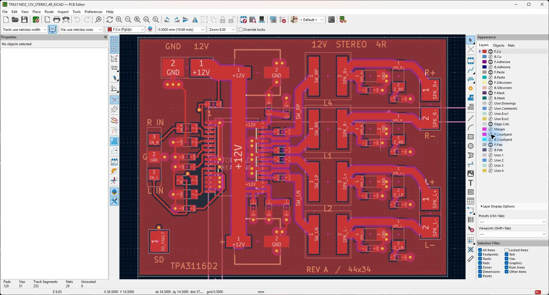
Figure: A KiCad PCB Editor screenshot
KiCad's command-line reference documents the ERC, DRC, parity, and export commands used here. Running them from a script made repeatable reports practical, since each writes its result to a file.
Libraries, Portability, and Automation: EasyEDA Pro vs KiCad
Both applications keep projects on the local disk and expose an automation interface, so the choice is narrower than cloud vs. desktop.
Keeping the Project Editable on Another Computer
The EasyEDA Pro delivers its schematic, PCB, and libraries within the native project, so it moves as a single file. EasyEDA documents local saving and offline modes in its local-export guide.
A KiCad project needs its companion files kept together, so portability was tested rather than assumed. The files were copied to a separate directory and rechecked there, returning zero findings in all four checks.
A KiCad release like this should include more than the board file. Four things are needed to travel with the project:
- The project file, both schematic sheets, and the PCB.
- The local symbol library, footprint directory, and both library tables.
- Any project-related 3D models are used by the design.
- A tested ZIP archive that has been extracted and reopened successfully to confirm the project is truly self-contained.
Choosing an Automation Interface
The KiCad side used local scripts and native command-line operations, and some Python API behavior had to be corrected during the run. Check those scripts against the installed version.
EasyEDA Pro provides a JavaScript extension API that this project did not use, so no comparison between the interfaces follows. Prefer interfaces returning inspectable results: saved files, netlists, and rule reports.
Manufacturing Files and Component Sourcing in EasyEDA Pro vs KiCad
EasyEDA Pro documents a PCB-order workflow that generates and uploads fabrication data, and its SMT tools help with part association. Their presence does not establish that this BOM is available for assembly.
The KiCad project exported its Gerbers, drills, BOM, and placement file fresh from the checked board, so the artwork matches the checked revision. Its drill report records 51 plated 0.30 mm holes and no unplated holes.
No board order, quotation, or factory DFM review was completed in either project. Before requesting assembly from either file set, work through five items:
- Check availability for every specified component in the JLCPCB parts library or your assembler's catalog.
- Resolve complete orderable part numbers and acceptable substitutions.
- Confirm that the 40 fitted components match the BOM and the placement file.
- Review coordinate conventions, rotations, and polarized parts against the assembly drawing.
- Inspect the exported copper, mask, paste, and drill layers for the revision being ordered.
A built-in order button should not decide which editor you use. What matters is a reviewed file set and a buildable BOM, and both tools can produce that.
Prompts That Improve AI-Generated PCB Projects
Naming an editor gives an agent direction, but it settles almost nothing about linkage, libraries, or the next revision. A useful prompt lists the native files and the verification evidence you expect to receive.
Six requirements are worth writing into a prompt of your own:
- State the supply, load, signal interfaces, component technology, and maximum board size.
- Name the editor and version, and ask for editable native schematic and PCB files.
- Require verified pin-to-pad mapping, included libraries, and copper that refills after an edit.
- Ask the agent to disclose autorouters, conversion steps, and any reused layout.
- Request the saved rule reports, the ignored categories, and the manufacturing exports.
- Say whether existing placement and routing must be preserved or may be redrawn.
Conclusion
Both projects reached the same TPA3116D2 amplifier, but the delivered files differ in how ready they are for the next revision.
The KiCad project is closer to a fully native, revision-ready design. Its schematic, libraries, component links, and GND zones remain editable, so future changes need less preparation.
The EasyEDA Pro project is also usable and keeps sourcing and ordering close to the editor, but this deliverable needs more cleanup before revision because its ground copper arrived as fixed-filled regions and its imported footprint identities required correction.
That does not prove KiCad is generally better than EasyEDA Pro. It only describes the condition of these two AI-generated projects. The next step is hardware validation. Both raw PCB outputs will first receive an engineering review, then be fabricated and assembled.
FAQs
Q: Which Is Better for PCB Design, EasyEDA Pro or KiCad?
This comparison does not answer that question because no timing or layout-quality measurements were taken. It compares two delivered projects of one amplifier, so it can only tell you what each file set lets you edit next.
Q: Do I Need Both Applications for a New PCB Project?
No. A new design can stay in one editor whenever that tool covers the schematic, board, and export work you need. Both applications appear here only because the same amplifier was delivered twice.
Q: Can a Gerber ZIP Replace the Native EasyEDA or KiCad Project?
No. Gerbers describe fabrication artwork, so they carry neither the editable schematic nor the symbol associations a revision needs. Keep the native project and its libraries beside every released manufacturing package.
Q: Does Moving Between EasyEDA Pro and KiCad Change the Amplifier?
Changing the editor does not affect electrical behavior, since both projects use the same circuit and board. Any claim about output power, distortion, or temperature needs measurements on an assembled board under defined conditions.
Popular Articles
• AI PCB Design: From Prompt to PCB with EasyEDA Pro
• AI Tools for PCB Design: Which Tool Fits Your Workflow Stage?
• GPT-6 Astra PCB Design in KiCad: From Brief to Verified Native Project
• GPT-6 Astra PCB Design in EasyEDA Pro: What Worked, What Failed, and What We Learned
• How to Design Your Own Keyboard PCB: From Layout to Firmware
Keep Learning
AI Tools for PCB Design: Which Tool Fits Your Workflow Stage?
AI tools can now assist with PCB architecture, schematic generation, component selection, placement, routing, and design verification. However, different tools target different stages of the PCB workflow. This guide compares AI tools for PCB design based on what they actually do, what inputs they require, and where they fit within a real engineering workflow. In this guide, you will learn: The 6 types of AI PCB tools and the input each one needs What AI PCB design tools do, compared stage by stage How......
Free Online Circuit Simulator for Electronics Engineers
Key Takeaways Simulate First: Free circuit simulators prevent fried components and cut PCB re-spins. Fix AC Sweep: Enter pure numbers for points per decade, not time units. Use SMD Parts: Swap ideal models for standard SMD resistors and SOT-23 transistors. Control Parasitics: Board trace capacitance and via inductance alter high-frequency signals. Verify Before Order: Pair SPICE simulation with DFM checks to ensure board success. If all electronic engineers had a dollar for each burnt-out resistor or ......
Mastering PCB Design Rules: A Comprehensive Guide for Optimal Results
Key Takeaways Follow core PCB design rules for reliable electrical and mechanical performance. Optimize trace width, spacing, impedance, and vias for signal integrity and manufacturability. Apply DFM and DRC early to identify potential manufacturing and layout issues. Consider thermal management, grounding, and testing during the PCB design stage. Align design rules with your PCB manufacturer’s capabilities to improve production reliability and reduce redesigns. PCB design rules are essential guidelin......
KiCad MCP: How to Design a PCB with Claude Code [Step-by-Step]
Key Takeaways Claude can design PCBs in KiCad: By connecting Claude to KiCad through an MCP server, you can use AI to create and modify PCB designs. In this project, Claude helped turn a 5 A XL4015 buck converter netlist into a two-layer, 63 × 33 mm PCB layout with zero ERC violations and zero DRC errors after minor initial fixes. Set up Claude securely: Use a KiCad MCP server that starts in read-only mode. Review the server code before installing it, connect through stdio, and allow editing only in a......
Claude Code PCB Design: Can It Build a Real Board in EasyEDA Pro?
Key Takeaways Claude Code PCB design: Using Claude Opus 5.5 and EasyEDA Pro 3.2.149, I converted a 47-component, three-page schematic from a PDF into a fully routed, two-layer PCB with zero DRC errors. EasyEDA Pro integration: The EasyEDA API skill connects Claude Code to EasyEDA Pro through a local bridge server and the Run API Gateway extension. This allows Claude to control the editor via JavaScript, with a 30-second timeout per API call. Design verification: A successful API response doesn't alway......
How to Design a PCB with Flux.ai (Step-by-Step Guide)
Key Takeaways This step-by-step Flux PCB design tutorial demonstrates the complete workflow by creating a compact 15 × 15 mm USB 2.0 hub, refining the layout, routing high-speed differential traces, and preparing manufacturing files for JLCPCB PCB fabrication and assembly. We are all hearing news; new AI models are being released every month. And it has finally reached the schematic editor. Flux.ai is a browser-based AI PCB design tool with a built-in AI agent that behaves like a junior hardware engin......