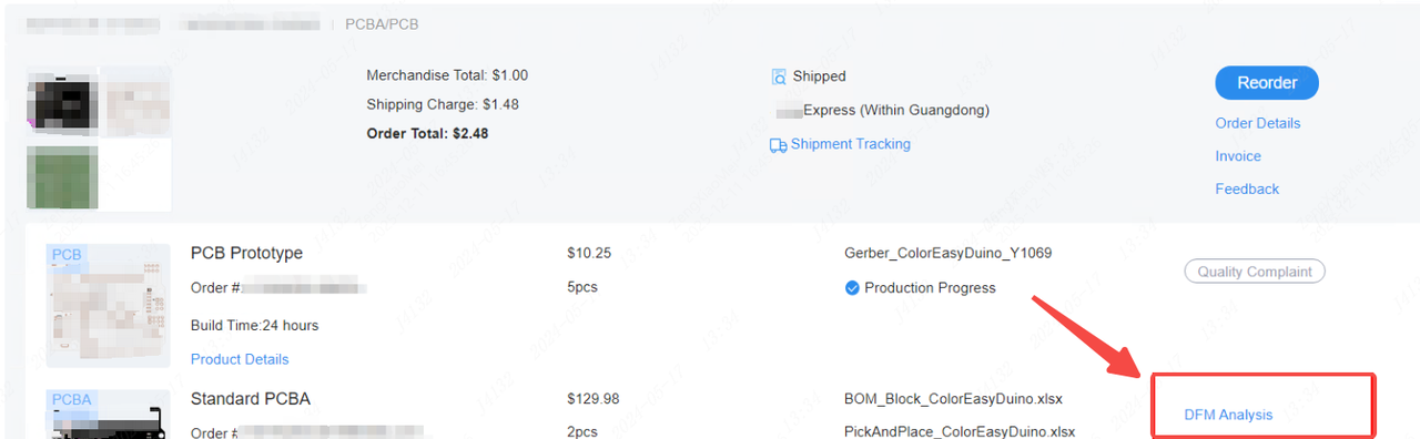
SMT After-Sales Customer Self-Inspection Guide
Last updated on Jan 26, 2026
Dear Valued Customer,
Before contacting our technical support team, we strongly recommend that you take a few minutes to perform a quick preliminary inspection of the affected PCBA following the steps outlined below.
This process may help you identify and resolve common issues quickly and will also significantly improve the efficiency of subsequent technical support.
⚠ Important: Please ensure that the board is completely powered off before performing any inspection.
Step 1: Visual Inspection
This is the most direct and fundamental check, intended to identify any obvious physical or cosmetic issues.
1. Overall Condition
Check whether the PCBA surface is clean and free from visible contamination, such as stains, moisture marks, mold, or foreign objects (e.g., solder balls, metal debris).
We use no-clean solder paste, which is designed to minimize post-soldering residues and typically does not require cleaning after reflow. Therefore, under normal circumstances, assembled boards are not cleaned by default, and minor flux residue may be present.
2. Board Integrity
- Inspect the PCB for cracks, fractures, warpage, or severe scratches.
- Check the board edges for burrs, chipping, or mechanical damage.
3. Traces and Copper Features
- Observe whether any traces show signs of lifting, delamination, or blistering.
- Check critical traces and pads for corrosion or oxidation, which may appear as abnormal discoloration.
4. Silkscreen and Identification
- Verify that the board part number and the order number on the packaging label are clear and legible.
- Confirm that the markings match the model and order you placed.
Step 2: Soldering Defect Inspection
Soldering-related issues are a primary cause of poor electrical contact or short circuits. Please inspect carefully.
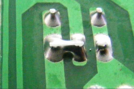
1. Solder Bridging / Shorts
Focus on fine-pitch components (such as QFP or SOP packages) and check whether solder has bridged adjacent pins, forming unintended connections.
Note:
Please review whether the pad dimensions in your design are oversized or excessively elongated.
For fine-pitch components, oversized pads reduce the effective isolation distance between pads, significantly increasing the risk of solder bridging.
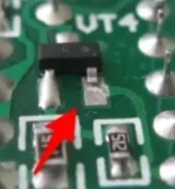
2. Cold Solder / False Solder Joints
- Check whether there is insufficient solder between component leads and pads, or if solder joints appear ball-shaped and poorly wetted.
- Gently nudge larger components (such as electrolytic capacitors or connectors) to check for looseness (do not apply excessive force).
Note:
Please verify that the pad size and geometry match the component terminals.
Mismatch between component leads and PCB pads may result in insufficient solderable area or uneven stress distribution, leading to cold or false solder joints.
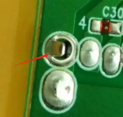
3. Insufficient Solder / Open Joints
- Check for solder joints where no solder is present, leaving component leads electrically floating.
- Pads that are too small, especially for larger or heavier components, may fail to provide adequate solder volume for mechanical strength and electrical connectivity.
Note:
Please check whether your pad design includes vias within pads (via-in-pad).
Vias on pads can cause solder to wick into the holes during reflow, resulting in insufficient solder.
Additionally, undersized pads—particularly for larger or heavier components—may not provide sufficient solder volume.
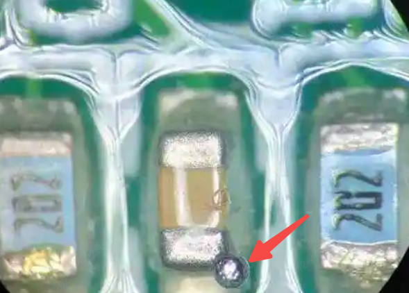
4. Excess Solder / Solder Balls
Observe whether excessive solder has formed large solder domes, or if loose solder balls are present on the board, both of which may cause short circuits.
Note:
Please verify whether the clearance between component bodies and pads is too small, which may restrict proper flux outgassing and cause solder paste extrusion or bridging. Also check for via-in-pad structures that have not been properly filled or capped.
Unfilled vias may draw solder into the holes during reflow, resulting in insufficient pad solder while also generating solder balls or voids.
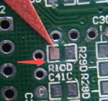
5. Lifted or Detached Pads
Inspect whether any PCB pads have lifted or detached from the laminate, which may occur during soldering or rework operations.
Step 3: Component Inspection
Check whether the components themselves have been incorrectly installed or physically damaged.
1. Incorrect or Missing Components
Compare the assembled components against the BOM or reference/sample images to verify that the part numbers, specifications, and values are correct, and confirm that no components are missing.
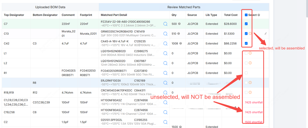
Please review the Selected Parts List in your order. JLCPCB assembles only the components explicitly selected in the order. Components that are not selected will not be assembled.
How to check:
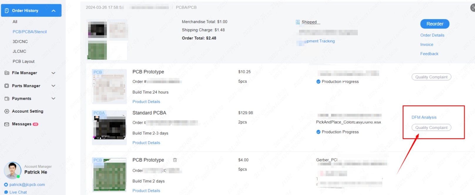
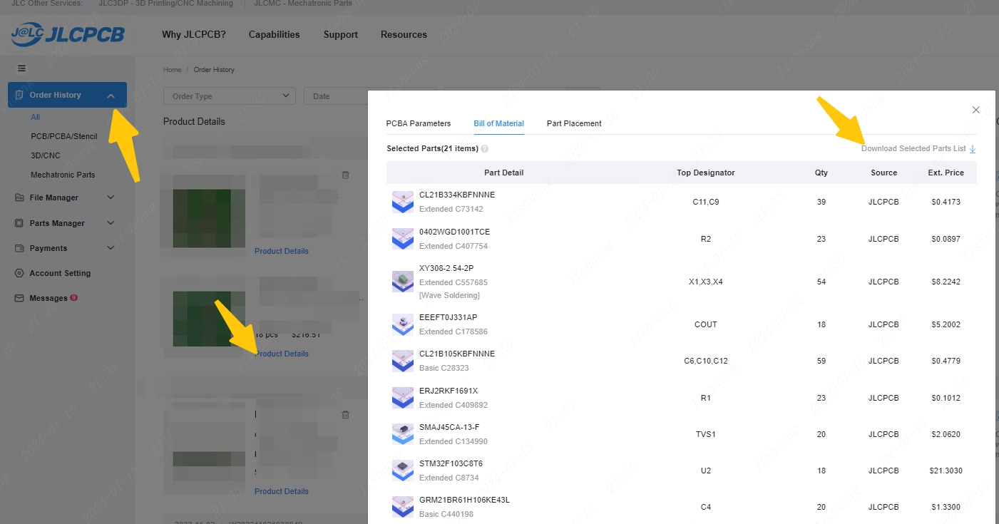
Go to Order History → locate the order → click Product Details → review the Bill of Materials (BOM) or download the Selected Parts List.
3. Polarity and Orientation
- Refer to the DFM files in your order to verify the orientation of polarized components, such as electrolytic capacitors, diodes, LEDs, IC sockets, and ICs.
- Polarity indicators on the PCB (e.g., “+” symbol, outline box, chamfered corner) should be consistent with the markings on the components.
For common polarity and orientation identification methods, please refer to the Component Polarity / Orientation Identification Guide.
3. Component Damage
Inspect components for visible signs of damage:
- Capacitors: Check for bulging or cracking on the top, and leakage at the bottom.
- Resistors / Inductors: Check for cracks, discoloration, or burn marks.
- ICs: Check for surface cracks, physical damage, burn pits, and inspect leads for oxidation or bending.
- Crystal Oscillators: Check for cracks or breakage.
If no abnormalities are found during the above checks, but component-level functional issues persist, we recommend submitting a PCBA Component After-Sales Claim Form.
Please note that failure analysis (FA) can be complex and highly design-dependent. While our technical team will make every effort to assist in verification, we may not be fully familiar with all circuit designs and application scenarios. Therefore, we cannot guarantee a definitive root cause analysis in all cases.
If the issue is determined to be a component functional failure, customers are advised to proceed with the PCBA Component After-Sales Claim Form.
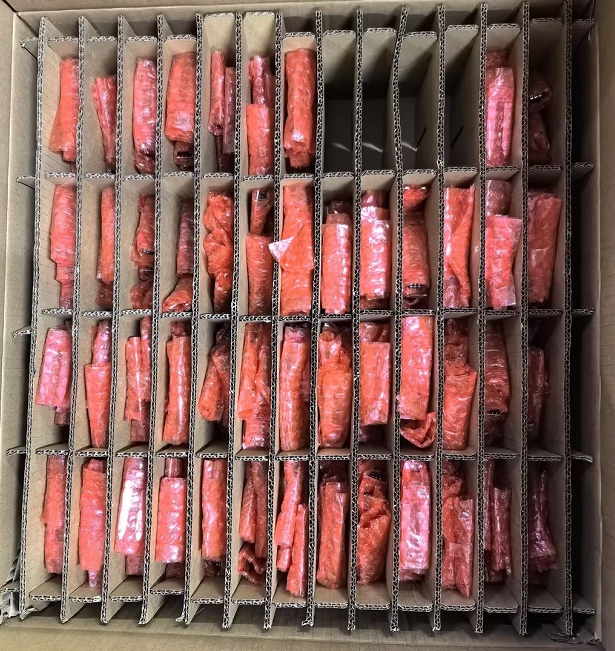
Step 4: Packaging and Transportation Inspection
Improper packaging or transportation may result in PCBA damage or surface scratches.
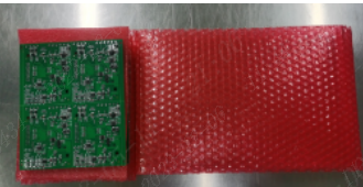
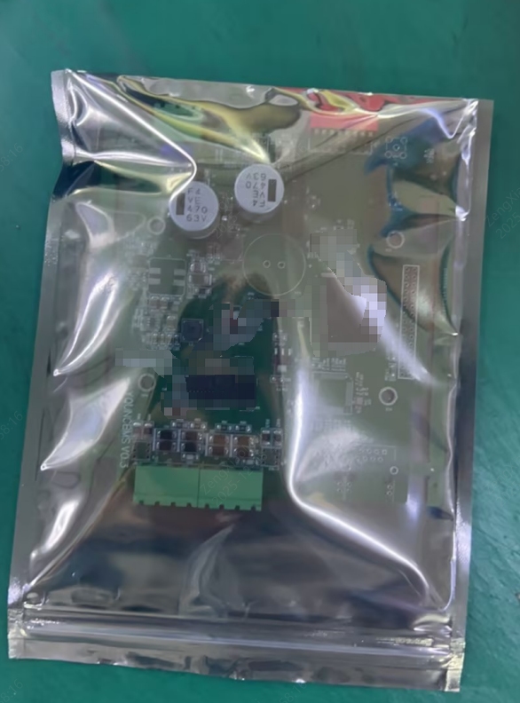
1. Bubble Wrap or ESD Protection
By default, PCBA orders are packaged using bubble wrap. If ESD bag packaging was selected for your order, please confirm that anti-static bags were used and that the bubble wrap provided adequate protection.
Bubble wrap packaging:
ESD bag packaging:
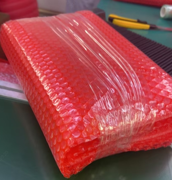
2. Cushioning and Fixation
Check whether the shipping carton contains sufficient cushioning materials (such as bubble pads or foam) and whether the PCBA was securely fixed inside the box without excessive movement.
(Pallet-style packaging shown as reference image)
3. Signs of Physical Damage
Inspect the packaging bags and cartons for signs of compression, puncture, tearing, or moisture exposure.
4. Storage Conditions
If the PCBA was stored before use, please confirm that the storage conditions met requirements: dry environment, room temperature, and protection from direct light.
High humidity may cause moisture absorption, which can lead to the “popcorn effect” during subsequent soldering or rework.
After Completing the Inspection
1. If Issues Are Identified
- If you have clearly identified the issue (e.g., bulging capacitors, solder bridging) and have rework capability, you may attempt corrective action.
- If you are uncertain, please document the issue and submit an after-sales request with detailed descriptions, photos, and/or videos. We will review the case and discuss compensation accordingly.
2. If No Obvious Issues Are Found
Please prepare the following information and submit an after-sales support request:
- PCBA Order Number: ______
- Affected PCB(s) / Reference Designator(s) and Quantity: ______
- Detailed Description of the Failure Symptoms: ______
- Self-inspection Steps Performed and Results: ______
- Ability to Perform Self-Rework (Yes / No): ______
Required Visual Evidence:
- High-resolution photos of the entire PCBA (front and back)
- Close-up photos of the affected area
- Video showing the abnormal behavior or failure symptom
Measurement Data:
Voltage and resistance readings at critical test points