Custom FPC Fabrication: Design Rules & Manufacturing Guide
16 min
- What Is Custom FPC Fabrication?
- Custom FPC Materials, Layer Stackups, and Construction Options
- Critical DFM Guidelines for Custom FPC Design
- Step-by-Step Custom FPC Manufacturing Process
- Custom FPC Quality Control and Reliability Testing
- What Affects Custom FPC Fabrication Cost and Lead Time?
- JLCPCB Custom Flexible PCB Capabilities and Specifications
- How to Prepare and Order a Custom FPC for Fabrication
- Conclusion
- FAQs About Custom FPC Fabrication
Custom FPC fabrication is the process of making flexible printed circuits in accordance with a customer's design requirements, such as board outline, layer stackup, copper thickness, openings for coverlay, and stiffener placement. Custom flexible circuits differ from traditional rigid PCBs in that they must be carefully designed and planned for materials and layout to meet flexibility and stress requirements and to fit into smaller assemblies. These design decisions are directly related to manufacturability, reliability, production cost, and lead time, and therefore need to be finalized before the design is submitted for fabrication.
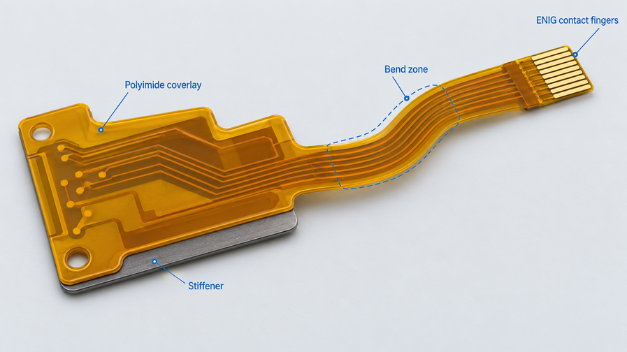
Figure: Custom FPC fabrication example showing a polyimide flex circuit with ENIG connector fingers
This guide will help you choose the right number of layers, laminate materials, copper foil, coverlay, and stiffeners for your custom FPC design. The key fabrication, inspection, and testing processes, as well as the factors that impact manufacturing costs and lead times, will also be explored, along with essential bend-radius, trace-routing, and coverlay design rules.
What Is Custom FPC Fabrication?
In custom FPC fabrication, you don't purchase a catalog flexible flat cable; you use the design-specific information to make one. The outline, stackup, and features are based on customer files, and the fabricator runs its normal process.
Understanding Custom Flexible Printed Circuits
There are five design inputs to determine a custom flexible PCB:
- Outline: A laser-cut contour, including tails, slots, and cutouts.
- Copper layout: Routing on one, two, or more copper layers.
- Stackup: Base film, copper weight, and coverlay, which sets the thickness and bend capability.
- Stiffeners: Bonded support plates under connectors and components.
- Connector interface: Contact fingers for a ZIF connector, or pads for a soldered joint.
Types of Custom FPCs: Single-Sided, Double-Sided, and Multilayer
Layer count is the first construction decision, because it sets thickness, flexibility, and routing capacity.
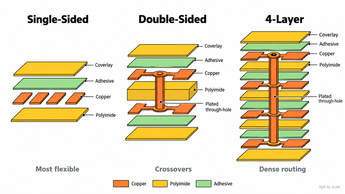
Figure: Custom FPC stackup comparison of single-sided, double-sided, and 4-layer constructions
| Construction | Structure | Advantage | Limitation | Typical Use |
| Single-sided | One copper layer on polyimide | Thinnest and most flexible | No routing crossovers | Hinges and printer head cables |
| Double-sided | Copper on both sides, joined by plated through-holes | Crossovers and a ground layer | Stiffer in the bend | Sensor tails and display links |
| Multilayer | Three or more copper layers bonded with adhesive films | Dense routing and shielding | Largest bend radius | Dense interconnects in compact devices |
Custom Flex PCB vs. Standard Flex vs. Rigid-Flex
A standard flat flex cable is bought by catalog dimensions, a custom FPC is built from your files, and a rigid-flex board is a different construction:
| Option | Buyer Specifies | Rigid Sections |
| Standard flat flex cable | Length, pitch, and contact count | None; it plugs into a connector at each end |
| Custom FPC with stiffeners | Outline, routing, stackup, and stiffeners | Bonded stiffeners only, with no circuitry |
| Rigid-flex PCB | Rigid and flex stackups | Flex layers laminated into rigid sections and joined by plated through-holes |
Custom FPC Materials, Layer Stackups, and Construction Options
The material stack decides how far a custom FPC can bend, how it survives soldering, and what it costs. Choose each layer for the bend type:
| Material Choice | Static Bend (Formed Once) | Dynamic Bend (Repeated Flexing) |
| Base laminate | Adhesive-based or adhesiveless polyimide | Adhesiveless polyimide |
| Copper foil | ED or RA copper | RA copper |
| Copper layers in the bend | One or two | One or two, preferably one |
| Protective layer | Coverlay or flexible solder mask | Polyimide coverlay |
Polyimide and PET Substrates: Adhesive-Based vs. Adhesiveless Laminates
Polyimide has been chosen as the default flex dielectric because it maintains its properties at soldering temperatures. PET is a transparent, cheaper film, but check the lower temperature rating against the reflow profile.
- Adhesive-based: Copper is fused with acrylic or epoxy adhesive. Less expensive, but adhesives increase thickness and swell with heat, putting strain on plated holes.
- Adhesiveless: Copper bonding to the polyimide. Thinner, more dimensionally stable, and preferred for dynamic flexing and fine features.
A 50 µm base film will provide better tear resistance; a 25 µm base film will provide a thinner, more flexible stack.
Copper Foil Selection: Rolled-Annealed vs. Electrodeposited Copper
- Rolled-annealed (RA) copper: grains within the material are elongated and will not allow crack growth to occur with repeated bending. According to JLCPCB's bend radius guide, RA copper is recommended for bending in dynamic applications.
- Electrodeposited (ED) copper: This is less expensive and is appropriate for static bends, but regular grades break after a few cycles.
The thinner the foil, the less strain at a given radius, and the best choice of copper weight for the tail is the thinnest that can carry the current of the tail.
Coverlay, Flexible Solder Mask, and Surface Finish Options
- Polyimide coverlay: Polyimide film with adhesive, lamination over the circuit. It can be bent repeatedly, but its openings are cut first, and then laminated, thus requiring a larger clearance for pads.
- Rigid solder mask: A photoimageable mask that can create small openings accurately and is suitable for fine-pitch pads in non-flexible application areas.
Industry flex finishes include ENIG, OSP, immersion silver, and hard gold on contact fingers. JLCPCB's flex capability is only ENIG 1-layer or 2-layer with 1 or 2 µin gold.
FPC Stiffeners: FR4, Polyimide, and Stainless Steel
A local area is supported by a stiffener that sets the thickness at connectors. These are the options that JLCPCB lists:
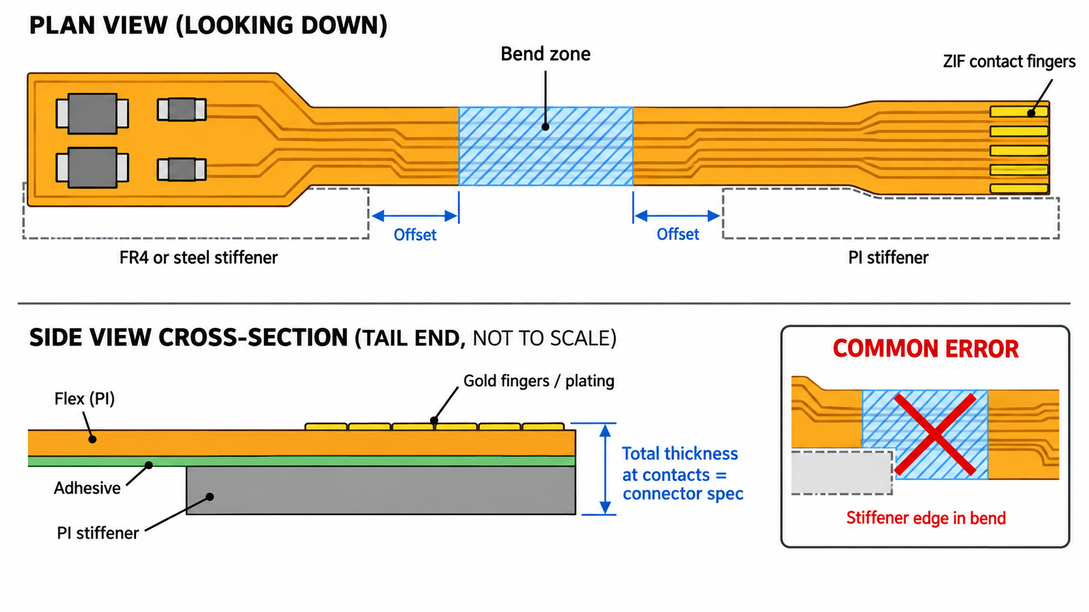
Figure: Custom FPC stiffener placement under ZIF connector fingers and a component area, with stiffener edges outside the bend zone.
| Stiffener | Main Purpose | JLCPCB Thickness | Design Note |
| Polyimide | Contact thickness at ZIF fingers | 0.1–0.25 mm | Match the connector datasheet |
| FR4 | Supports connectors and components | 0.1–1.6 mm | Edges can chip |
| Stainless steel | Keeps SMT areas flat in a thin profile | 0.1–0.3 mm | Costs more; slightly magnetic, so keep it away from Hall-effect sensors |
| Adhesive tape | Secures the FPC in the housing | 3M 468, 3M 9077, tesa 8854 | 3M 468 is not heat-resistant |
Critical DFM Guidelines for Custom FPC Design
Custom FPC design rules link the layout to what the fabricator can build and what the circuit can survive in service, primarily around the bend zone and minimum feature sizes.
Bend Radius, Flex Cycles, and Neutral Axis Considerations
Bend radius is measured at the inside surface of the bend as a multiple of finished thickness. JLCPCB publishes two sets of multipliers:
- Minimum, from the capabilities page: Static bends at 6× for single-layer and 10× for multilayer circuits. Dynamic bends at 10–15×.
- Conservative, from the flexible PCB bend radius guide: Static bends at 6× and 12×. Dynamic bends at 100× for single-layer and 100–150× for multilayer. The guide adds a 20–30% safety margin to the calculated minimum.
Use the minimum for a bend formed once during installation. Use the conservative value for a dynamic bend or any bend without flex-test data, and confirm the cycle life on prototypes.
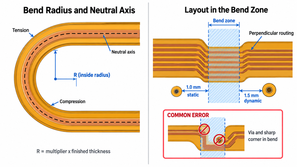
Figure: Custom FPC bend zone design showing inside bend radius, neutral axis, perpendicular trace routing, and via keep-out distances.
Calculation for a 2-layer circuit, finished thickness: 0.12 mm - one of the listed options of JLCPCB:
- Static minimum: 10 × 0.12 mm = 1.2 mm.
- Static conservative: 12 × 0.12 mm = 1.44 mm, or about 1.7–1.9 mm with the margin.
- Dynamic conservative: 100–150 × 0.12 mm = 12–18 mm before the margin.
The plane inside a bent stack that is not strained is called the neutral axis. Placing a single copper layer near the coverlay is an attempt to balance the two. A two-layer circuit has the copper on both sides of the axis and thus requires a larger bend radius.
Trace Routing, Via Placement, and Copper Fracture Prevention
The flex PCB design guide covers most of these rules:
- Route perpendicular to the bend line: This minimizes strain on the copper.
- Use curved corners: Replace 90° corners and abrupt changes in width with arcs.
- Stagger traces on opposite layers: Offset top and bottom traces to lower stiffness through the bend.
- Keep vias and pads out of the bend: The bend radius guide recommends at least 1.0 mm from the bend-zone boundary for static bends and 1.5 mm for dynamic bends.
- Add teardrops: Use them on pad-to-trace and via-to-trace joints in flexible areas.
- Hatch copper planes: A hatched plane flexes more easily than a solid pour.
Trace Width, Spacing, Hole Sizes, and Edge Clearances
Design to JLCPCB's regular values, and use a limit value only where a feature needs it:
| Feature | Regular Value | Absolute Limit or Note |
| Trace/space, 12 µm copper | 3/3 mil | 2/2 mil absolute limit; below 3 mil adds a fee |
| Trace/space, 18 µm copper | 3.5/3.5 mil | Regular value |
| Trace/space, 35 µm copper | 4/4 mil | Regular value |
| Via hole/pad | 0.3/0.55 mm | 0.10/0.3 mm (2-layer) or 0.15/0.35 mm (4-layer), extra cost |
| PTH annular ring | 0.25 mm | 0.18 mm minimum |
| Copper to board edge | 0.3 mm or more | Also applies to slots |
| Gold finger pad to edge | 0.2 mm | Closer fingers are cut back |
Step-by-Step Custom FPC Manufacturing Process
A custom FPC will undergo CAM review, imaging, hole formation, coverlay, finishing, stiffener bonding, profiling, and testing. A single-sided circuit without plated holes only requires a single-sided circuit, while a 4-layer circuit requires inner-layer lamination.
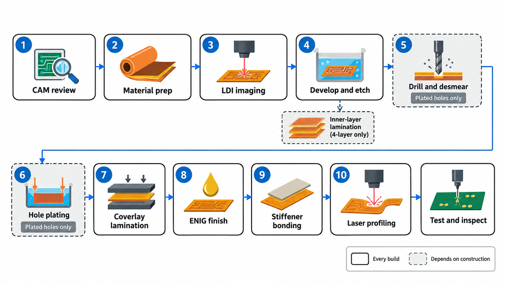
Figure: Custom FPC fabrication process flowchart with numbered stages
Step 1: CAM Review, Material Preparation, and Copper Imaging
CAM engineers review the data, ask engineering questions if it is incomplete, and cross-check it against the stated stackup. The laminate is cut, and then dry-film photoresist is applied. Laser direct imaging (LDI) exposes the pattern and scales each panel to the measured targets to compensate for the film's dimensional change. Forming and etching the copper circuit.
Step 2: Drilling, Desmear, and Copper Plating
Hole formation depends on the construction:
- Mechanical drilling: Through-holes in double-sided and multilayer circuits.
- UV laser drilling: Microvias and very small holes.
- Single-sided circuits: Any holes are unplated, so desmear and plating are skipped.
Plasma or chemical desmearing cleans the walls of the drilled hole before metallization. Electroless copper or direct metallization then makes them conductive, and electroplating builds the barrel.
Step 3: Coverlay Lamination and Surface Finishing
Coverlay openings are precisely laser-drilled or punched, then laminated with a heated press to align with the pads. Openings are enlarged so that adhesive can flow slightly into them. The exposed copper is then finished with the surface.
Step 4: Stiffener Bonding and Precision Outline Cutting
Stiffeners are glued with a thermosetting adhesive under heat and pressure, or with a pressure adhesive. Then, by using the CAM data, the outline, slots, and cutouts are cut out by a laser without a cutting die. JLCPCB will provide the protective PET film free of charge if the board is narrower than 2 mm or wider than 20 mm, unless the customer does not want to accept the curl risk.
Step 5: Inspection, Electrical Testing, and Final Delivery
- AOI: Compares etched copper with the CAM data.
- Electrical test: Checks continuity and isolation against the netlist.
- Final inspection: Confirms outline, coverlay alignment, and stiffener position.
- Packaging: Vacuum packing with desiccant, because polyimide absorbs moisture.
Custom FPC Quality Control and Reliability Testing
Custom FPC quality control covers acceptance of the built circuit against a specification, and qualification of the design for its service life.
IPC-6013 Standards and Manufacturing Acceptance Requirements
IPC-6013 is the qualification and performance specification for flexible and rigid-flex printed boards. It uses three performance classes:
- Class 1: General electronic products.
- Class 2: Dedicated-service products, where uninterrupted service is desired but not critical.
- Class 3: High-performance products, where continued operation is critical.
The class is set in the procurement documents and is not applied by default, so agree on it with the fabricator for critical applications. IPC-2223 is the companion design standard.
AOI, Flying Probe, and Fixture-Based Electrical Testing
| Method | What It Detects | Best Fit |
| AOI | Opens, shorts, nicks, and width deviations on each layer | Every layer, before lamination, hides it |
| Flying probe | Continuity and isolation, with moving probes and no fixture | Prototypes and small batches |
| Fixture test | The same checks, with all points contacted at once | High volumes that spread the fixture cost |
What Affects Custom FPC Fabrication Cost and Lead Time?
Custom FPC cost is set mainly by panel area, layer count, and quantity, then raised by special features. Lead time depends on the construction and on how quickly engineering questions are answered.
Main Cost Factors in Custom Flexible PCB Manufacturing
- Panel utilization: Price follows the panel area the outlines occupy, including waste.
- Layer count: Each layer adds imaging, plating, or lamination steps.
- Materials and features: Film type, copper weight, fine trace and space, small vias, and hole count.
- Finishing: ENIG area and thickness, stiffeners, and EMI shielding film.
- Quantity: One-time setup is shared across the order.
Prototype vs. Small-Batch vs. Mass-Production Costs
The flex PCB cost guide describes how the dominant cost shifts with volume:
- Prototype, 5–20 pieces: Setup and tooling dominate.
- Small batch, 500–2,000 pieces: Material and panel yield dominate.
- Mass production (10,000+ pieces): Raw polyimide and copper areas dominate.
Typical Production Lead Times and Turnaround Factors
Lead time is the build time in the factory, and shipping is added after it. JLCPCB's homepage listed a 5–6-day build time for flexible PCBs at the time of writing, and the quote reflects the build time for the selected options.
Turnaround commonly extends with:
- 4-layer construction: An additional lamination cycle.
- Several stiffener materials: A bonding step for each material.
- Engineering queries: Missing stiffener or coverlay data pauses the order.
- Assembly: Component availability adds to the total.
JLCPCB Custom Flexible PCB Capabilities and Specifications
JLCPCB builds custom flexible PCBs on polyimide or transparent PET film, with ENIG finish and laser-cut outlines. It does not build rigid-flex boards or offer impedance control on flex.
Supported Layer Counts, Thicknesses, Materials, and Surface Finishes
These values come from JLCPCB's flex PCB capabilities page:
| Parameter | JLCPCB Published Capability |
| FPC layers | 1, 2, and 4 |
| Base material | Polyimide, 25 or 50 µm, adhesive or adhesiveless; transparent PET, 36 µm |
| Copper thickness | 12, 18, or 35 µm (single-sided: 18 or 35 µm) |
| Finished thickness | 0.07–0.2 mm for 1- and 2-layer polyimide; 0.2–0.45 mm for 4 layers |
| Minimum regular trace/space | 3/3 mil with 12 µm copper |
| Surface finish | ENIG, 1 or 2 µin gold |
| Coverlay colors | Yellow, black, white, and transparent |
| Stiffeners | PI, FR4, stainless steel, and adhesive tape |
| Regular maximum dimensions | 234 × 490 mm |
| Outline tolerance | ±0.1 mm; ±0.05 mm on request |
| Flex impedance measurement and control | Not currently supported |
| True rigid-flex boards | Not currently supported |
How to Prepare and Order a Custom FPC for Fabrication
A custom FPC order requires complete fabrication data, a design checked against the fabricator's limits, and notes on which Gerber layers cannot be shown.
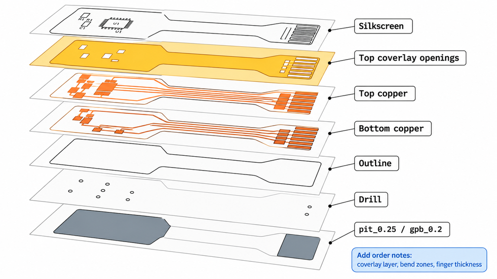
Figure: Custom FPC fabrication file set showing copper, coverlay-opening, outline, drill, and named stiffener layers in an exploded view.
Required Manufacturing Files and Documentation
- Gerber files: RS-274X copper, solder mask, silkscreen, and outline layers.
- Drill data: An Excellon file for plated and non-plated holes.
- Coverlay openings: On the solder mask layers or on a separate layer, as specified in the order notes.
- Stiffener layers: Filled polygons, one layer per material, side, and thickness, named as in the FPC stiffener guide, such as pit_0.25 for 0.25 mm top PI or gpb_0.2 for 0.2 mm bottom steel.
- Fabrication drawing: Stackup, finished thickness, bend zones, and connector-finger thickness.
EasyEDA Pro adds two dedicated stiffener layers to a project setup as a rigid PCB and automatically updates the Gerber files after placing a stiffener. Where the fabricator confirms it will accept formats such as ODB++ or IPC-2581, then they must be used.
Conclusion
The key to successful FPC custom fabrication is a well-planned design that accounts for flexibility, reliability, manufacturability, and cost. Choosing the correct laminate, copper foil, and layer stackup is as important as determining the correct bend radii, coverlay openings, stiffener locations, and connector requirements. By adhering to these specifications within your manufacturer's standard production capabilities, you can minimize fabrication difficulties, avoid unnecessary manufacturing expenses, and increase the reliability of the finished flexible circuit.
Always check design rules, stackup, and critical dimensions, and document all manufacturing requirements before placing the order. A full and accurate fabrication package is key to avoiding production delays, unexpected costs, and design revisions. After your custom FPC design is complete, you can request a quote and proceed with prototyping or production.

FAQs About Custom FPC Fabrication
Q. What Is the Minimum Bend Radius for a Custom Flex PCB?
Ans: It depends on thickness, layer count, and bend type. JLCPCB's static minimums are 6× for single-layer and 10× for multilayer circuits, while its bend-radius guide recommends 100× or more for dynamic bends.
Q. How Many Layers Can a Custom FPC Have?
Ans: Flex circuits range from single-layer copper to multilayer stacks of three or more layers. JLCPCB builds 1-, 2-, and 4-layer custom FPCs. Fewer layers in the bend allow a smaller bend radius.
Q. What Materials Are Commonly Used in Custom Flexible PCBs?
Ans: Most use a polyimide-based film, RA or ED copper, and a polyimide coverlay. PET is a lower-cost, transparent alternative, and stiffeners are usually made of polyimide, FR4, or stainless steel.
Q. How Do I Choose Between FR4, PI, and Stainless Steel Stiffeners?
Ans: Use PI to set the thickness at the ZIF connector fingers, FR4 to support connectors and components, and stainless steel where a thin SMT area must remain flat. Steel is more expensive and slightly magnetic.
Q. How Much Does Custom FPC Fabrication Cost?
Ans: There is no fixed price. Panel area, layer count, and quantity set the base, and stiffeners, large ENIG areas, and fine traces add to it. JLCPCB lists 2-layer flex boards up to 100 × 100 mm for $2.00 for 5 pieces.

Keep Learning
Best Flex PCB Design Software: CAD Tools & Setup Guide
The right flex PCB design software would rely on the complexity and construction of your circuit. Altium Designer, Cadence Allegro X, OrCAD X, and Siemens Xpedition are professional tools that offer advanced capabilities for flexible and rigid-flex PCB designs, such as stackup management, bend regions, and mechanical constraints. In the meantime, for more basic flexible circuits, tools such as KiCad or EasyEDA Pro might be viable options, though they may require some manual setup and verification. Fle......
Custom FPC Fabrication: Design Rules & Manufacturing Guide
Custom FPC fabrication is the process of making flexible printed circuits in accordance with a customer's design requirements, such as board outline, layer stackup, copper thickness, openings for coverlay, and stiffener placement. Custom flexible circuits differ from traditional rigid PCBs in that they must be carefully designed and planned for materials and layout to meet flexibility and stress requirements and to fit into smaller assemblies. These design decisions are directly related to manufactura......
Polyimide Flexible PCB Fabrication: Materials and Process Guide
Polyimide flexible PCB fabrication is a process of creating thin polyimide film and copper-foil-based circuits that will bend, fold, and withstand soldering temperatures. But the same flexibility that comes from the thin film material used on these boards, and which is sensitive to moisture, makes production slightly more difficult than rigid PCBs. Polyimide can expand or contract during processing, absorb moisture before reflow soldering, and suffer from copper fatigue or cracking if the bend radius ......
Flexible PCB Price: Key Cost Factors and Ways to Save
The price of a flexible PCB has no single fixed figure, as it depends mainly on the panel area occupied by the design, the number of copper layers, and the order quantity. Other features such as stiffeners, EMI shielding film, tight outline tolerance, and a complex via structure may further increase manufacturing costs. The majority of these cost factors are fixed by the PCB layout stage, and even at the time of the first quotation. Figure: Polyimide flexible PCB with ENIG contact pads and a bonded st......
Flex PCB Design Guide: Preventing Mechanical Failures
Key Takeaways Reliable flex PCB design requires more than electrical performance. Proper bend radius control, trace routing, via placement, stiffener selection, and DFM considerations are essential to prevent mechanical failures such as copper cracking and delamination. By following proven flexible PCB design practices, engineers can improve durability and achieve reliable production results with JLCPCB. Ever wonder how the circuit in a foldable phone, fitness tracker, or camera module manages to rema......
FPC Electronics: What Is It, How It Works, Applications, and Benefits
FPC electronics is the reason your phone camera still works after a hundred open-and-close cycles. Peel apart almost any modern device, and you will find a thin amber ribbon carrying signals around corners no rigid board could turn. In this guide, you will learn: What does FPC stand for, and what are the differences between FFC and FPC? A flexible circuit that conducts a signal as it flexes The materials include one polyimide, copper, coverlay, and stiffener FPC manufacturing process (etching to elect......