
Choosing the Right Bend Radius for Durable Flexible PCBs
14 min
- Understanding Bend Radius in Flexible PCB Design:
- How to Determine the Proper Bend Radius:
- Design Best Practices for Optimal Bend Radius:
- Manufacturing Considerations for Reliable Flexible PCBs:
- JLCPCB's Expertise in Flexible PCB Bend Radius:
- FAQ about Bend Radius
- Conclusion:
Key Takeaways
Mastering the bend radius is essential for reliable flexible PCB design. Following IPC-2223 guidelines, maintain a minimum of 6× total thickness for static bends and 100× for dynamic applications, while using thinner RA copper, adhesiveless polyimide, staggered traces, and cross-hatched patterns in flex zones. Proper material selection, layer stackup optimization, and adequate clearance from stiffeners can dramatically extend flex life and prevent premature trace cracking or delamination.
Have you ever bent a strip of paper in half till it tore in half along the line? And that is what occurs in a flexible PCB when the radius of bending is excessively small. The copper traces fracture, the polyimide substrate becomes weak, and your previously dependable circuit has turned into a time bomb that has just one fuse to blow in the field. Flexible printed circuits are ubiquitous nowadays, with the folding screen on your smartphone, the ribbon cables in your laptop, and the sensor arrays in your wearable health monitor. The bend radius is the most important parameter in each of these products that can make the difference between a long-life design and a design that collapses after a couple of hundred cycles. Make a mistake, and you are staring at broken traces, peeled off coverlays, and costly field returns. In this tutorial, we are going to take you through all the details of selecting, computing, and testing the correct bend radius of your flexible PCB. We will discuss IPC standards, choice of material, design practices, design errors to avoid, and how contemporary manufacturers can maintain bend radius conformity in the fabrication process.
Understanding Bend Radius in Flexible PCB Design:
What Bend Radius Is and Why It Matters for FPC Reliability
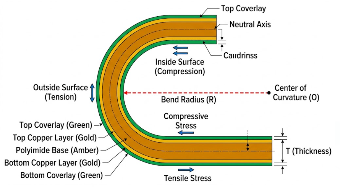
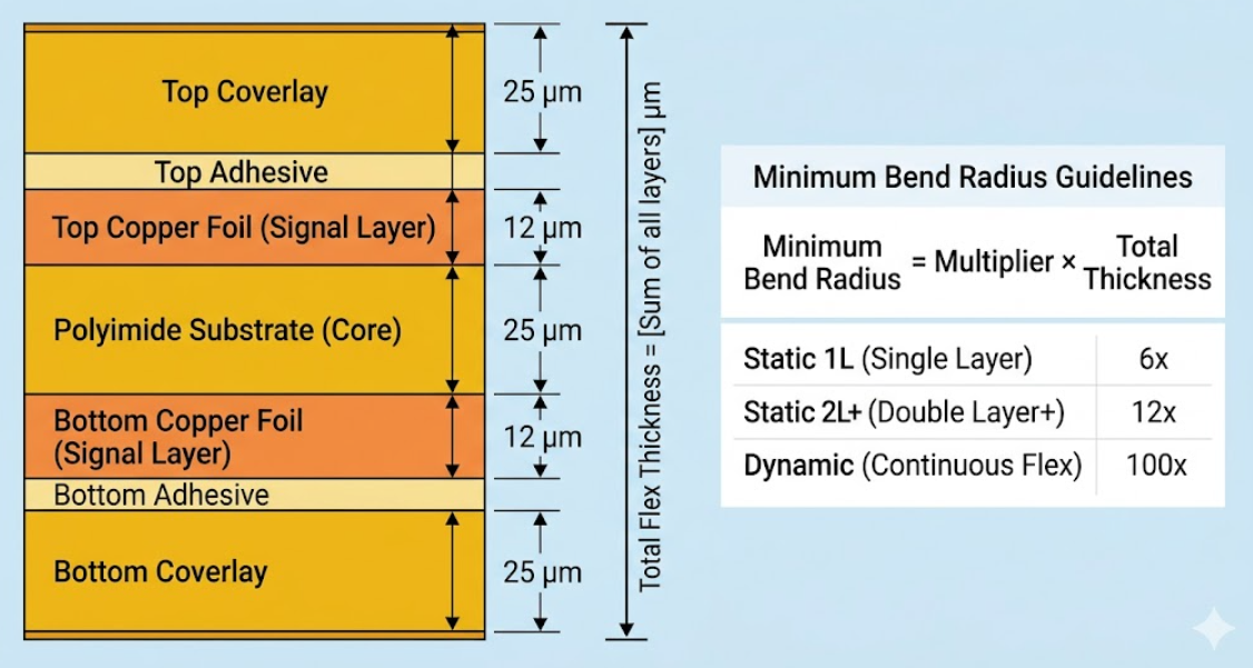
The radius of the tightest arc that a flexible circuit can be bent without mechanical damage is the FPC bend radius. Consider wrapping a flex circuit around a cylinder. The radius of that cylinder is called the radius of bend, and this is always measured on the inside surface of the bend to the center of curvature. Why is this so important? As a flex PCB is bent, the outer part of the bend is subjected to tensile stress (stretching), and the inner part to compressive stress. These stresses should not crack or delaminate the copper traces and polyimide substrate. When the radius of the bend is too small, the stress is beyond the capability of the material, and it fails. The sectional design standard of flexible and rigid-flex printed board, IPC-2223, dictates the minimum possible bend radius based on three important factors, including the overall thickness of the flex construction, the number of conductor layers, and the type of bend, which can be static or dynamic. This relationship is non-negotiable to have a reliable flex circuit design.
Dynamic vs. Static Bend Radius Requirements
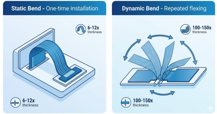
Not every bend is created equal, and this is where most engineers err first. A one-time bend is a bend made during the product installation, where the flex circuit is bent and remains in place throughout the product's life. A dynamic bend is a flex circuit that needs to flex in and out multiple times in a normal operation, e.g., the hinge of a folding phone or the print head cable of a printer. The disparity between the minimum bend radius requirements of these two categories is dramatic. The following is a brief comparison according to IPC-2223 guidelines:
| Application Type | Layers | Minimum Bend Radius |
|---|---|---|
| Static (single layer) | 1 | 6x total flex thickness |
| Static (multilayer) | 2+ | 12x total flex thickness |
| Dynamic (single layer) | 1 | 100x total flex thickness |
| Dynamic (multilayer) | 2+ | 100-150x total flex thickness |
How to Determine the Proper Bend Radius:
Standard Guidelines and Industry Recommendations
The base of any bend radius calculation is the sum of the overall thickness of the flexible part of your circuit. This is all: the polyimide substrate (usually 12.5 to 50 micrometers), the copper foil layers (usually 12 to 35 micrometers each), the adhesive layers (when using adhesive-based laminates), and the coverlay on both sides (usually 25 to 50 micrometers each).
The overall equation of IPC-2223 is as follows:
Minimum Bend Radius = Multiplier x Total Flex Thickness.
The multiplier is dependent on how you use it:
- The multiplier to use when there are single-layer static bends is 6.
- In the case of multilayer static bends (two or more layers), a multiplier of 12 should be used.
- The multiplier to use is 100 when it comes to single-layer dynamic bends.
- In the case of multilayer dynamic bends, a multiplier of 100 to 150 should be used.
An additional 20-30% safety margin on the calculated minimum is also a best practice. Stresses can be added by manufacturing tolerances, lot variations in materials, and assembly handling, and this is not considered in your calculations. A design that performs well in simulation may not perform well in production.
How to Measure Bend Radius Accurately
It is imperative that both designers and quality engineers know how to measure bend radius. The bend radius is always calculated with respect to the inside surface of the flex circuit being bent, not with respect to the outside surface, and not with respect to the neutral axis.
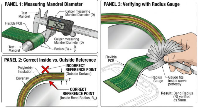
The following is a step-by-step procedure to measure the bend radius of a physical flex circuit:
- Wrap the flex circuit around a mandrel or cylindrical shape of known radius.
- Make sure that the flex is lying flat on the mandrel and that it is not creased or wrinkled.
- Measure the radius of the mandrel. This is your bend radius.
- In the case of free-form bends with no mandrel, a radius gauge or optical measuring system is used to measure the inside radius of curvature.
- Ensure that the measured radius is at least as large as your design minimum with the safety margin.
The bend radius is normally specified in the mechanical design files or flex zone properties in EDA tools. EasyEDA, Altium Designer, and KiCad, among others, enable you to define bend zone radii, so your design is aware of the mechanical constraints early on.
Design Best Practices for Optimal Bend Radius:
Layer Stackup, Material Selection, and Transition Zone Design
Your layer stackup determines the tightness of your flex circuit. The following are the main principles:
- Keep the number of layers in the bend zone to a minimum. Each extra layer increases the thickness, and thus the minimum bend radius. Neck down to fewer flex region layers, when possible in your design.
- Where possible, use adhesiveless (cast) laminates. Adhesive layers provide thickness and may be delaminated through repeated bending. Polyimide laminates are adhesiveless, which offer thinner constructions and reliability.
- Use thinner copper foils in bends. A copper foil with a 12-micrometer diameter bends much more easily than a foil of 35 micrometers. Use the thinnest copper that meets your electrical requirements in the flex zone.
- With dynamic applications, use rolled annealed (RA) copper. As mentioned above, the grain structure of RA copper is oriented to prevent fatigue cracking when bending repeatedly.
Another critical area is the transition zone between the rigid and flexible areas of a rigid-flex PCB. A sudden change forms a point of concentration of stress at the point of flex of the rigid section. The most effective way is to create a progressive taper or bevel at this interface, and not to place vias, pads, or plated through-holes within 1.5 mm of the boundary of the bend zone.
| Design Parameter | Static Application | Dynamic Application |
|---|---|---|
| Copper type | RA or ED | RA only |
| Recommended copper weight | 0.5-1 oz | 0.5 oz |
| Coverlay material | Polyimide | Polyimide |
| Adhesive type | Acrylic or epoxy | Acrylic (preferred) |
| Minimum trace width in the bend | Standard DRC | Wider traces preferred |
| Via-to-bend-zone clearance | 1.0 mm min | 1.5 mm min |
Avoiding Common Mistakes That Reduce Flex Life
Even seasoned designers can fall into the traps that undermine flex circuit reliability. The following are the most frequently used errors and their prevention:
- Stacking traces directly on top of each other in multilayer flex. The traces on the top and bottom layers form a stiff I-beam structure when they are in direct contact with each other, and they do not bend or diffuse stress. Rather, alternate the traces such that traces on the top are between the bottom traces. This maintains flexibility and distributes stress more uniformly.
- Using solid copper pours in the bend area. A strong copper planar in the bend area radically enhances rigidity and is nearly assured to fracture during dynamic bending. Instead, use copper patterns using cross-hatched patterns with standard parameters of 0.38 mm (15 mil) trace-width and 0.63 mm (25 mil) spacing. Cross-hatching eliminates a large fraction of the copper area, and still allows flexibility, yet has a return current path.
- Putting the components or stiffeners too near the bend. Rigid points are formed by components and stiffeners. If they are too close to the bend zone, they act as stress concentrators. A minimum of 2.5 mm should be the clearance between any rigid component and the beginning of the bend region.
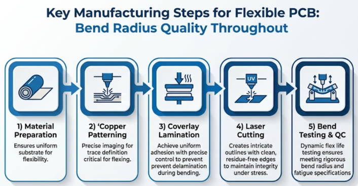
Manufacturing Considerations for Reliable Flexible PCBs:
Precision Fabrication and Coverlay Application
To produce a flexible PCB that satisfies its bend radius requirement, it is important to be precise at each stage of the fabrication process. The flex circuit equivalent of solder mask on a rigid board is the coverlay, a laminated polyimide film, adhesively backed. It prevents oxidation, moisture, and mechanical abrasion of copper traces. Bend reliability is especially important when using the coverlay application. The coverlay should be smooth and without any holes, wrinkles, or air bubbles. Any opening in the coverlay leaves a weak point exposing the copper trace below it to no protection, and stress concentration during bending may begin a crack at that very point.
Quality Control to Ensure Bend Radius Compliance
Flex PCBs require quality control beyond the normal AOI and electrical testing of rigid boards. The compliance of the bend radius is to be mechanically validated. The Qualification and Performance Specification of Flexible and Rigid-Flexible Printed Boards, IPC-6013, specifies the testing of flex circuits in three performance classes:
Class 1: General electronic products (consumer devices)
Class 2: Dedicated service products (industrial, communications)
Class 3: Military, medical, aerospace products (high reliability)
In dynamic flex applications, IPC-6013 provides qualification testing that incorporates dynamic flex testing as specified in IPC-TM-650 Method 2.4.3 of bending the circuit to its designated radius thousands of times and then checking whether or not there are cracks, delamination, or changes in resistance. A standard test protocol will involve surviving 10,000 cycles at the given bend radius at 20 mm.
JLCPCB's Expertise in Flexible PCB Bend Radius:
Advanced Capabilities for Complex Flexible Designs
JLCPCB has a complete range of capabilities designed to ensure reliability when it comes to producing flexible PCBs with the capability to bend around demanding bend radius requirements. Their flexible PCB service allows 1 to 4-layer constructions and polyimide substrate thicknesses of 25 and 50 micrometers, allowing designers the option to tune their stackup to their desired bend radius requirements. JLCPCB applies 100% adhesive-free base material to their flex PCBs, which is a huge benefit to bend radius performance. As we have already mentioned, adhesive layers contribute to the thickness and may delaminate when bending repeatedly. It allows JLCPCB flex constructions to be thinner and more dependable in bend areas by removing the adhesive.
The largest board size of 234 x 490 mm can hold even the large flex circuit design, and the manufacturing process is very precise, such that the copper thickness and coverlay application throughout the panel are uniform. Their flex coverlay can achieve more than 200,000 bends without cracking, and the polyimide substrate can work up to 280 degrees C. These specifications are not just numbers on a datasheet. They are directly converted into the field reliability of products that rely on flexible circuits.
Proven Reliability for Dynamic and Static Flex Applications
Your application needs a single, simple, static bend to route your cables inside an enclosure or a challenging, dynamic flex to make a folding consumer device. The manufacturing process at JLCPCB provides similar results. They have a quality control process that involves checking coverlay adhesion, uniformity of copper plating, and dimensional accuracy of flex zones. To engineers who are interested in applying the principles of bend radius design, the flexible PCB service offered by JLCPCB is a good and affordable way to go from prototype to production. Beginning with competitive prices and quick turnaround times, they make it feasible to repeat your flex design until the bend radius performance is precisely where it should be.
FAQ about Bend Radius
Q: What is the minimum bend radius for a flexible PCB?
The minimum bend radius depends on the total thickness of the flex construction and whether the application is static or dynamic. For single-layer static bends, the minimum is typically 6 times the total flex thickness. For dynamic bends, it increases to 100 times the total thickness or more. Always add a 20-30% safety margin to the calculated minimum.
Q: What is the difference between static and dynamic bend radius?
A static bend occurs once during assembly, and the flex circuit remains in that position permanently. A dynamic bend involves repeated flexing during normal product operation. Dynamic bends require a much larger minimum bend radius, typically 100 to 150 times the flex thickness, compared to 6 to 12 times for static bends.
Q: How do I measure bend radius on a flexible PCB?
Bend radius is measured from the inside surface of the bent flex circuit to the center of the arc. The most accurate method is to bend the flex around a mandrel of known radius and verify that it is seated flush. For free-form bends, use a radius gauge or optical measurement system. Never measure from the outside of the bend, as this will overestimate the actual bend radius.
Q:Can I use electrodeposited copper in dynamic flex applications?
No. Electrodeposited (ED) copper has a columnar grain structure that makes it brittle under repeated bending. Rolled annealed (RA) copper is required for dynamic applications because its elongated grain structure provides significantly better fatigue resistance.
Q: Why should I use cross-hatched copper instead of solid planes in the bend area?
Solid copper planes in the bend zone dramatically increase stiffness and will crack under repeated bending. Cross-hatched patterns remove a significant portion of the copper area, preserving flexibility while still providing a functional return current path. Typical cross-hatch parameters are 0.38 mm trace width with 0.63 mm spacing.
Q: What IPC standards cover flexible PCB bend radius?
IPC-2223 is the primary design standard for flexible and rigid-flex PCBs and defines minimum bend radius requirements. IPC-6013 is the qualification and performance specification that covers testing requirements.
Conclusion:
Bend radius is not an empty design check box. It is the base of any dependable flexible PCB. Whether it is the knowledge of the basic difference between the requirements of a static or dynamic bend or the correct routing of the traces in the bend area and the verification of the performance by IPC-6013 testing, all the decisions made in the design and manufacturing chain will lead to the final outcome. The main lessons can be easily summarized: initialize with the IPC-2223 multipliers, add a 20-30% safety factor, always use rolled annealed copper in dynamic applications, route traces perpendicular to the bend axis, stagger traces in multilayer designs, and use cross-hatched patterns in the bend area.
Popular Articles
• 45 Must-Know Flex PCB Design Tips You Can't Afford to Miss!
• Choosing the Right Bend Radius for Durable Flexible PCBs
• FPC Design Rules: 13 Safety Distances You Can’t Ignore
• Mastering PCB Stiffeners: A Comprehensive Guide to Types, Applications, and Design Best Practices for Flexible Circuits
• How Flex Coverlay Protects and Enhances Flexible PCB Durability
Keep Learning
Flex PCB Manufacturing Process: From Prototyping To Mass Production
Flexible Printed Circuit Board commonly known as flex PCBs are a revolutionary step in modern electronics that offer compact, lightweight, dynamic and precise designs. Flex PCBs are designed to bend, twist, and fold, which rigid boards are incapable of. These characteristics have led to their widespread adoption in industries like wearable technology to consumer electronics to aerospace and medical technologies. With demands increasing day by day for miniaturized and ergonomic product designs, underst......
45 Must-Know Flex PCB Design Tips You Can't Afford to Miss!
Achieving perfection in product design requires a careful balance between meeting design requirements and manufacturing standards. However, when it comes to flex PCB (FPC) design, many engineers find themselves at a loss, unsure of where to begin. In this insightful guide, we will delve into 45 essential design guidelines for FPC. By the end, you'll have the knowledge and confidence to navigate the complexities of flex PCB design. Outline and Drilling 1. The minimum distance from through-holes to the ......
Choosing the Right Bend Radius for Durable Flexible PCBs
Key Takeaways Mastering the bend radius is essential for reliable flexible PCB design. Following IPC-2223 guidelines, maintain a minimum of 6× total thickness for static bends and 100× for dynamic applications, while using thinner RA copper, adhesiveless polyimide, staggered traces, and cross-hatched patterns in flex zones. Proper material selection, layer stackup optimization, and adequate clearance from stiffeners can dramatically extend flex life and prevent premature trace cracking or delamination......
FPC Connector Guide: Types, Pitch & Reliability
Key Takeaways Choosing the right FPC connector is critical for reliable flexible electronic designs. Connector type, pitch, pin count, stiffener thickness, and PCB layout all affect signal integrity and mechanical durability. By understanding FPC connector selection and design considerations, engineers can reduce connection failures and achieve reliable assembly results with JLCPCB. As you know, the electronics world is getting smaller; nowadays, the devices need to be thin and light. All the parts sh......
Flex PCB Design Guide: Preventing Mechanical Failures
Key Takeaways Reliable flex PCB design requires more than electrical performance. Proper bend radius control, trace routing, via placement, stiffener selection, and DFM considerations are essential to prevent mechanical failures such as copper cracking and delamination. By following proven flexible PCB design practices, engineers can improve durability and achieve reliable production results with JLCPCB. Ever wonder how the circuit in a foldable phone, fitness tracker, or camera module manages to rema......
Flex PCB Prototyping Guide: Materials & Design Tips
Key Takeaways A reliable flex PCB prototype requires more than just a working circuit. Material selection, bend radius control, copper design, panelization, and stiffener choices directly impact flexibility, durability, and manufacturing success. By following proper flexible PCB prototyping practices, engineers can reduce design risks and smoothly transition from prototypes to production with JLCPCB. Ever wonder how the circuit in a smartwatch, a foldable phone, or a camera module can take the shape? ......