
Flex PCB Design Guide: Preventing Mechanical Failures
12 min
- Understanding Mechanical Stress in Flexible PCB Designs
- Via and Trace Routing Considerations for Bend Areas
- Bend Radius and Reinforcement Design Strategies
- Material and DFM Considerations for Reliable FPCs
- JLCPCB's Expertise in Flexible PCB Manufacturing
- Frequently Asked Questions (FAQ)
Key Takeaways
Reliable flex PCB design requires more than electrical performance. Proper bend radius control, trace routing, via placement, stiffener selection, and DFM considerations are essential to prevent mechanical failures such as copper cracking and delamination. By following proven flexible PCB design practices, engineers can improve durability and achieve reliable production results with JLCPCB.
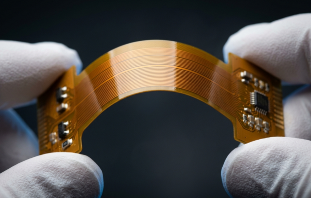
Ever wonder how the circuit in a foldable phone, fitness tracker, or camera module manages to remain intact after thousands of folds without cracking? The magic lies in good Flex PCB Design, which is as much about mechanical engineering as it is about electrical routing. A flexible circuit never sees the same world of constant motion, tension, and compression that a rigid board does. The majority of flex circuit failures are not electrical in nature. They are mechanical and can almost always be traced back to a few design errors that are avoidable, such as around bends, vias, and material selections.
After a few thousand flex cycles, the copper cracks, the via barrels fatigue, or the laminate delaminates. I will guide you through the mechanical stress created by flexible PCB designs, the importance of vias and trace routing in bend zones, and the role of bend radius, stiffeners, and DFM checks to ensure reliable boards. Let's get into it and create real-life, long-lasting flex circuits.
Understanding Mechanical Stress in Flexible PCB Designs
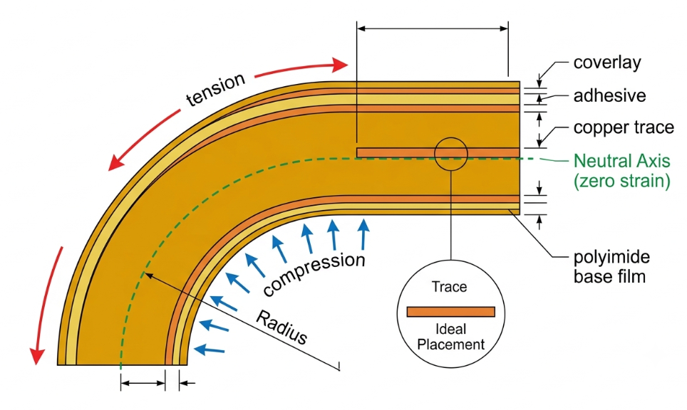
Each bend of the flex PCB causes the outside to be stretched and the inside to be compressed. The copper traces are much less ductile than the polyimide base and are directly in the way of this strain. If that stress is repeatedly applied beyond the copper's elastic limit, micro-cracks develop that increase in size until a crack appears. The first step to avoiding failure is to know where the stress is occurring. A flex circuit is not equally stressed under stress. It accumulates at the transitions, edges, and anywhere there is a sharp change in the flexibility of the board.
Common Mechanical Failure Mechanisms in FPC Applications
With a little knowledge of what to look for, flexible circuits can fail in predictable ways. More often than not, field returns are one of these.
- Copper trace cracking: Tension on the outside (outside) of a bend causes fatigue of the conductors, often causing cracking.
- Delamination: The adhesive or coverlay comes off the base film as a result of repeated stress or thermal cycling.
- Solder joint failure: Stress and fracture are focused on the flex-to-rigid solder joint transition, which is a rigid solder joint.
- Coverlay cracking: The protective polyimide layer separates due to a bend radius that is too tight.
Static vs Dynamic Flex PCB Design Considerations
Not every flex circuit experiences the same mechanical stresses, and your design rules should take that into account. The difference between static and dynamic applications is the basis for nearly all decisions downstream. A static flex application will only bend a few times, typically when it is being installed, and remains stationary. Imagine a flex board folded in half and put inside a camera case. Dynamic flex is an application where the flex is continually flexed during its service life, such as the hinge cable in a laptop or the ribbon in a printer head.
| Parameter | Static Flex | Dynamic Flex |
|---|---|---|
| Flex cycles | <100 (install only) | Thousands to millions |
| Minimum bend radius | 6x material thickness | 20x to 100x material thickness |
| Copper type | Standard ED copper | Rolled annealed (RA) copper |
| Layer count | 1 to multilayer | Typically, 1 or 2 layers |
| Copper in the bend zone | Allowed with care | Single layer, centered on the neutral axis |
Via and Trace Routing Considerations for Bend Areas
When it comes to Flex PCB Design, routing is where the reliable boards are separated from the warranty nightmares. The bend area is the most mechanically active part of the circuit and requires special routing discipline. The simple rule is this: Bend zone – make it as uniform and flexible as possible. Stress risers are created by anything that increases the local stiffness in a bend area. This applies to vias, dense parallel copper, and component pads. The idea is to allow the flex region to flex in a uniform, smooth piece.
Why Vias and Parallel Traces Reduce Flexibility
The number one enemy to a healthy bend zone is a via. A plated via is a rigid copper cylinder that is glued through the laminate and cannot bend with the surrounding film. During the bending of the board, the strain is focused on the via barrel and the surrounding pad, which results in barrel cracking or pad lift. A related issue is when traces are packed tightly in parallel. The large, solid copper strip that passes through the bend is akin to a stiffener and increases the rigidity in the area, which increases the strain in the spaces between the traces. This leads to irregular bending and cracking of the copper edges. Therefore, one basic guideline of flexible PCB design is to avoid positioning vias within a bending region. Ensure that all vias, pads, and dense copper are located in the rigid or static sections of the board, away from the bending area.
Routing Techniques for Better Mechanical Durability
Proper routing in a flex circuit is not about focusing the strain; it's about distributing it. There are some effective methods that can make a big difference for mechanical reliability.
- The route is perpendicular to the bend axis with each conductor crossing the fold at the shortest, straightest route, minimizing the length of copper under strain.
- In a brick-wall stagger, traces are not laid on top of each other on opposite layers; this decreases the effective stiffness through the bend.
- Avoid 90-degree corners as they are typical stress concentrators that fail first; use curved traces.
- Trying to vary the trace width across the bend area will result in stiffness discontinuities.
- Use a flex stackup with center critical copper to ensure that the most critical copper layer experiences the least strain.
Bend Radius and Reinforcement Design Strategies
If there is one number that defines flex circuit reliability, it is the bend radius. A too small radius will cause copper to exceed its strain limit, and a too large radius will keep all components in the safe elastic zone. It is then reinforced by elements that cope with stress at the transition between flex and rigid. When these two elements are correct, radius and reinforcement, most of the mechanical failures in flexible PCB designs are resolved. Let's do some number crunching and hardware analysis.
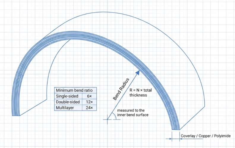
Recommended Bend Radius Guidelines
The minimum bend radius is a multiple of the total flex thickness and varies by the number of layers and the type of application. These ratios are taken from IPC-2223, the sectional design standard for flexible printed boards, and are industry-accepted starting points. The greater the radius, the longer the fatigue life. If possible, allow more space than the minimum (particularly in dynamic designs). As a general guideline, each additional millimeter of radius will give you useful cycle life.
Using Stiffeners and Teardrop Pads to Reduce Stress
Stiffeners are rigid materials, usually stainless steel, FR4, or polyimide, that are glued to the flex circuit at certain points. They don't increase the flexibility of the board. Rather, they preserve areas that do not require any flex at all, like connector areas, component-mounting areas, and the critical transition point between flex and rigid. The most crucial stiffener task is controlling the location of bending. Stiffening everything except the desired bend area will cause the flex to bend in that area only. This will avoid random folding, which can cause copper to crack in unexpected places.
- Add stiffeners under all connectors and component footprints.
- Stiffener edges should be placed away from the bend area, and offset such that the stiffness change does not occur at the flex point.
- Teardrop all pad-to-trace and via-to-trace connections in the flex.
- Apply filleted/radiused corners to copper pours around transitions.
Material and DFM Considerations for Reliable FPCs
No matter how perfect the layout is, if the material or manufacturing rules are incorrect, it will not work. Material selection provides a base level mechanical performance, and DFM checks catch issues that simulation may not. They work in combination to create a base for a manufacturable, reliable flex PCB. This is also where working closely with your manufacturer from the outset is beneficial. The right stackup and clearances are based on actual fabrication capabilities, not just textbook values.
Material Selection and Stackup Optimization
Polyimide is the workhorse base film for flexible circuits by virtue of its excellent thermal stability, dimensional stability, and flex endurance. Its dielectric constant is in the range of 3.2 – 3.5, and it can withstand soldering temperatures of more than 300 C. Polyimide is the most common material used in most flex PCB applications. The type of copper used is as important as the underlying film. The important material compromises you may consider in your stackup design are summarized below.
| Material Choice | Best For | Mechanical Note |
|---|---|---|
| Polyimide base | Nearly all flex | High flex endurance, stable to 300 C+ |
| Rolled annealed (RA) copper | Dynamic flex | Elongated grain resists fatigue cracking |
| Electrodeposited (ED) copper | Static flex | Lower cost, less fatigue-resistant |
| Adhesiveless laminate | Tight bends, fine pitch | Thinner stackup, better flexibility |
| Coverlay (polyimide) | Conductor protection | Flexes with the circuit, unlike the solder mask |
Minimize the thickness of the stackup and make it as symmetrical as possible. A thinner total thickness equates to a smaller radius of bend, and symmetry ensures that the neutral axis remains in the center, thereby minimizing strain on the copper. This is aided by the use of adhesive-less constructions, which eliminate a rigid adhesive layer in the sandwich.
DFM Checks for Mechanical Reliability
Design for Manufacturing in flex is not just about yield; it's about mechanical survival. Make sure you make these checks before you release your files.
- Check that no vias or plated holes lie within any bend zone or within the recommended keep-out distance of any bend zone.
- Ensure the bend radius is equal to or greater than the minimum bend radius as per IPC-2223 for the number of layers and type of flex.
- Ensure traces do not cross the bend at an angle and are routed in a curve.
- Make sure that teardrops are placed on all pads and via connections in flexible areas.
- Check stiffener location and overlap to ensure transitions are strengthened, and bend zones are clear.
- Verify coverlay openings and clearances against the manufacturer's capability.
The good DFM pass also verifies the copper balancing between layers and the good anchoring of pads near the flex-to-rigid boundary. It's much more cost-effective to pick these up on screen rather than after a flex cycle test failure.
JLCPCB's Expertise in Flexible PCB Manufacturing
When the board fabrication process doesn't match the solid design rules, the results aren't reliable. This is where an experienced flex manufacturer makes a difference in real-world durability. JLCPCB has developed significant expertise in flexible and rigid-flex printing and fabrication specifically for mechanical reliability. The challenge is not only to create a flex circuit, but to create one that will last through the flex circuit's intended bend life. That means close process control and engineering feedback during the building process.
Quality Inspection and Process Control
The reliability of a flex circuit can only be demonstrated by inspection and test. JLCPCB uses automated optical inspection (AOI) to detect trace defects, registration, and coverlay misalignment, which would reduce mechanical life. Electrical tests ensure continuity and isolation prior to boards leaving the factory.
Stackup thickness and copper geometry are consistent from board to board due to process control in lamination, etching, and coverlay bonding. That regularity is the reason that your calculated bend radius and neutral-axis routing really function as you intend. Once you're ready to step from the design phase into production, JLCPCB's flex and rigid-flex services allow you to easily fabricate boards capable of supporting up to actual mechanical stresses.

Frequently Asked Questions (FAQ)
Q: Why should vias never be placed in the bend area of a flex PCB?
Ans: A plated via is a rigid copper cylinder that cannot flex with the surrounding polyimide film. When the board bends, strain concentrates at the via barrel and pad, causing barrel cracking or pad lifting. Always keep vias in the rigid or static regions, away from the bend zone.
Q: What is the minimum bend radius for a flexible circuit?
Ans: Per IPC-2223, single-sided static flex needs at least 6x the material thickness, double-sided needs 12x, and multilayer needs 24x. Dynamic applications require much larger radii, often 20x to 100x or more, because fatigue accumulates over thousands of cycles.
Q: What is the difference between static and dynamic flex PCB design?
Ans: Static flex bends only a few times during installation and then stays fixed, allowing tighter radii and standard copper. Dynamic flex bends continuously throughout its service life, demanding rolled annealed copper, single-layer routing, and a much larger bend radius to survive repeated cycles.
Q: How do stiffeners improve flex PCB reliability?
Ans: Stiffeners are rigid backings bonded to the connector and component areas to prevent those zones from flexing. By stiffening everything except the intended bend region, they force the circuit to bend exactly where designed and protect solder joints from fatigue. Their edges should be offset from the bend zone.

Popular Articles
• 45 Must-Know Flex PCB Design Tips You Can't Afford to Miss!
• Choosing the Right Bend Radius for Durable Flexible PCBs
• FPC Design Rules: 13 Safety Distances You Can’t Ignore
• Mastering PCB Stiffeners: A Comprehensive Guide to Types, Applications, and Design Best Practices for Flexible Circuits
• How Flex Coverlay Protects and Enhances Flexible PCB Durability
Keep Learning
Flex PCB Manufacturing Process: From Prototyping To Mass Production
Flexible Printed Circuit Board commonly known as flex PCBs are a revolutionary step in modern electronics that offer compact, lightweight, dynamic and precise designs. Flex PCBs are designed to bend, twist, and fold, which rigid boards are incapable of. These characteristics have led to their widespread adoption in industries like wearable technology to consumer electronics to aerospace and medical technologies. With demands increasing day by day for miniaturized and ergonomic product designs, underst......
45 Must-Know Flex PCB Design Tips You Can't Afford to Miss!
Achieving perfection in product design requires a careful balance between meeting design requirements and manufacturing standards. However, when it comes to flex PCB (FPC) design, many engineers find themselves at a loss, unsure of where to begin. In this insightful guide, we will delve into 45 essential design guidelines for FPC. By the end, you'll have the knowledge and confidence to navigate the complexities of flex PCB design. Outline and Drilling 1. The minimum distance from through-holes to the ......
Choosing the Right Bend Radius for Durable Flexible PCBs
Key Takeaways Mastering the bend radius is essential for reliable flexible PCB design. Following IPC-2223 guidelines, maintain a minimum of 6× total thickness for static bends and 100× for dynamic applications, while using thinner RA copper, adhesiveless polyimide, staggered traces, and cross-hatched patterns in flex zones. Proper material selection, layer stackup optimization, and adequate clearance from stiffeners can dramatically extend flex life and prevent premature trace cracking or delamination......
FPC Connector Guide: Types, Pitch & Reliability
Key Takeaways Choosing the right FPC connector is critical for reliable flexible electronic designs. Connector type, pitch, pin count, stiffener thickness, and PCB layout all affect signal integrity and mechanical durability. By understanding FPC connector selection and design considerations, engineers can reduce connection failures and achieve reliable assembly results with JLCPCB. As you know, the electronics world is getting smaller; nowadays, the devices need to be thin and light. All the parts sh......
Flex PCB Design Guide: Preventing Mechanical Failures
Key Takeaways Reliable flex PCB design requires more than electrical performance. Proper bend radius control, trace routing, via placement, stiffener selection, and DFM considerations are essential to prevent mechanical failures such as copper cracking and delamination. By following proven flexible PCB design practices, engineers can improve durability and achieve reliable production results with JLCPCB. Ever wonder how the circuit in a foldable phone, fitness tracker, or camera module manages to rema......
Flex PCB Prototyping Guide: Materials & Design Tips
Key Takeaways A reliable flex PCB prototype requires more than just a working circuit. Material selection, bend radius control, copper design, panelization, and stiffener choices directly impact flexibility, durability, and manufacturing success. By following proper flexible PCB prototyping practices, engineers can reduce design risks and smoothly transition from prototypes to production with JLCPCB. Ever wonder how the circuit in a smartwatch, a foldable phone, or a camera module can take the shape? ......