Flex PCB Cost: Complete Pricing Guide & Ways to Reduce Costs
16 min
- Understanding Flex PCB Cost and Why Pricing Varies
- How Much Does a Flex PCB Cost? Pricing Overview and Calculation Factors
- Key Factors That Influence Flex PCB Cost
- Flex PCB Manufacturing Cost: From Design Files to Finished Boards
- Flex PCB Cost vs Rigid PCB Cost: Understanding the Differences
- How to Reduce Flex PCB Manufacturing Costs
- Choosing a Cost-Effective Flex PCB Manufacturer
- JLCPCB's Cost-Effective Flex PCB Manufacturing Capabilities
- Conclusion
- Frequently Asked Questions About Flex PCB Cost
Flex PCB cost is the number that stops most projects cold. You finish a clean polyimide design, upload the Gerbers, and the quote comes back at several times higher than what the same circuit would cost on FR4. Knowing which line items drive that number is what lets you bring it down.
In this guide, you will learn:
- Real flex PCB price ranges for prototypes and production
- The factors that move an FPC quote the most
- How does the layer count and quantity change per-board price
- Why flex costs more than rigid, and when it pays back
- How to read a flex PCB cost calculator
- Practical ways to cut manufacturing costs
Understanding Flex PCB Cost and Why Pricing Varies
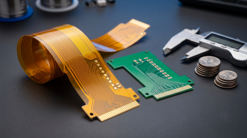
Pricing a rigid PCB is like buying flooring by the square meter. Pricing a flexible PCB is closer to tailoring a suit: the cloth is expensive, the cutting is fussy, and much of what you pay covers the work of making it fit. Two quotes for the same outline can differ by a factor of five.
What Determines the Cost of a Flexible PCB?
Flex PCB cost is set by five things: the panel area your design consumes, the layer count, the order quantity, the difficulty of the features, and the finishing options.
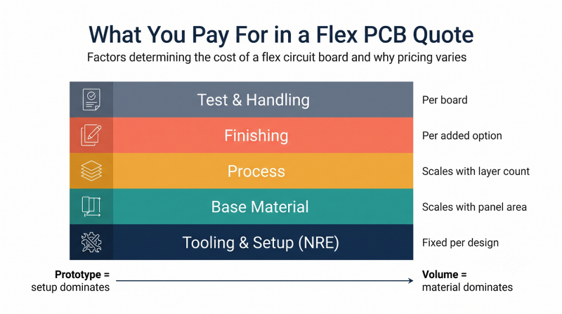
Only one is fixed: Tooling and setup (phototools, coverlay die or laser file, test fixture, and panel layout) costs are charged once per design for all board quantities purchased.
Why Flex PCBs Have Different Pricing Compared with Rigid PCBs
A rigid FR4 panel is a stiff sheet that machines handle at speed. A polyimide panel is a thin film that stretches, curls, and moves under heat. Other than this, polyimide costs several times more per unit area than woven glass epoxy. Coverlay openings must be cut and registered rather than printed like a solder mask. Dimensional movement during lamination lowers yield. And thin material demands slower handling at almost every station.
How Much Does a Flex PCB Cost? Pricing Overview and Calculation Factors
Per-board cost falls steeply between 5 and 500 units. At JLCPCB, flexible PCBs start from $25 for 5 pieces with a 4 to 5 day build, against $2.00 for 5 pieces and a 24-hour build on standard rigid FR4. That gap is the real flex premium at prototype scale.
Typical Flex PCB Price Range for Prototypes and Production
| Order Stage | Typical Quantity | How Cost Behaves | Practical Takeaway |
| Prototype | 5 to 20 pcs | Setup and tooling dominate | Order the full minimum; dropping 5 to 2 boards saves almost nothing |
| Engineering build | 50 to 200 pcs | Set up spreads out; steepest per-board drop | Best value point for design validation |
| Pilot run | 500 to 2,000 pcs | Material and panel yield dominate | Panel utilization now controls your cost |
| Volume | 10,000+ pcs | Raw polyimide and copper areas dominate | Every square millimeter removed pays back |
How Layer Count and Quantity Affect Flex PCB Price
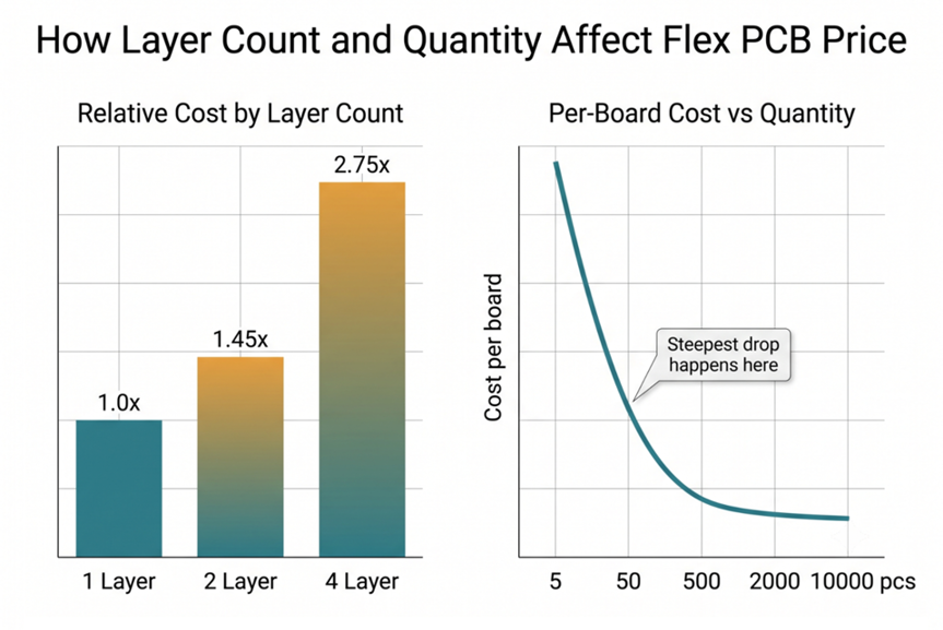
Layer count is the most aggressive multiplier in a flex quote. Each added layer brings its own imaging, etching, lamination, and registration cycle, typically 35 to 40 percent per layer.
| Layer Count | Relative Cost | What Changes in the Process | Best Suited To |
| 1 layer | Baseline | Single etch, coverlay one side, no plated vias | Jumpers, LED strips, sensor tails, dynamic bending |
| 2 layer | Roughly 1.4x to 1.5x | Plated through-holes, two-sided coverlay, registration control | Most interconnects, camera, and display tails |
| 4 layer | Roughly 2.5x to 3x | Sequential lamination, tighter registration, thicker stack | Controlled impedance, dense routing, shielded runs |
How to Calculate Flex PCB Cost with a Cost Calculator
A flex PCB cost calculator will quote your parameters on the capability matrix of the flex PCB assembly. No need to have completed Gerbers, just a desired outline and stackup is enough.
- Board dimensions and quantity: Use the real outline, not the bounding box.
- Layer count: Start at the lowest layer your routing needs.
- Dielectric thickness: Polyimide at 25 µm (1 mil) or 50 µm (2 mil) covers most designs.
- Copper weights: 12 µm (0.33 oz), 18 µm (0.5 oz), and 35 µm (1 oz) are standard.
- Coverlay color and stiffeners: Each stiffener zone adds a lamination step.
- Optional finishing: ENIG thickness, EMI film, and adhesive tape are priced separately.
- Two or three variants: Re-quote with one layer fewer, or a smaller outline.
Key Factors That Influence Flex PCB Cost
Material Selection, Substrate, and Copper Requirements
The most popular flex substrate remains polyimide film, also referred to by its trade name Kapton, which can withstand reflow and bend without cracking. There are two cost-laden decisions:
- Dielectric thickness: 25 µm is more flexible and is better for dynamic applications, while 50 µm is more stable for static applications, and is the more affordable and forgiving construction.
- Laminate: Adhesiveless laminate is thinner and more thermally stable, will tolerate fine pitch and repeated bending, and is meaningfully more expensive.
The standard and least costly is the electrodeposited (ED) copper. Rolled annealed (RA) copper does not crack with repeated flexing and is more expensive. Copper weight also sets your minimum feature size and with it your yield, as it does for a copper pour on a rigid board.
Layer Count, Board Size, and Circuit Complexity
Board size drives cost through panel consumption: what matters is how many boards fit one production panel.
Standard minimum trace and space tracks copper weight:
- 12 µm: 3/3 mil (0.075 mm) standard, with 2/2 mil as an absolute limit that costs yield
- 18 µm: 3.5/3.5 mil (0.089 mm), the best balance of density and price
- 35 µm: 4/4 mil (0.1 mm), more current but coarser routing, and a stiffer bend
Vias follow the same logic. A 0.3 mm drill with a 0.55 mm pad (11.8 / 21.7 mil) builds at normal cost, while a 0.10 mm drill with a 0.3 mm pad on two-layer flex carries a surcharge.
Surface Finish, Coverlay, Stiffener, and Manufacturing Requirements
Finishing options are where quotes quietly inflate; four together can add more than the base board. Flex almost always uses ENIG rather than HASL, because hot solder leveling would deform thin polyimide. It comes at 1 µin or 2 µin gold, and the thicker option buys shelf life you may not need. Stiffeners are most often over-specified. Pick the cheapest one that does the job.
| If You Need | Choose | Typical Thickness Range | Why |
| Support under an FPC connector insertion zone | Polyimide stiffener | 0.1 to 0.25 mm (3.9 to 9.8 mil) | Thin, matches connector spec, lowest cost |
| A rigid landing area for SMT components | FR4 stiffener | 0.1 to 1.6 mm (3.9 to 63 mil) | Handles reflow and mechanical load |
| Maximum stiffness in minimum thickness | Stainless steel | 0.1 to 0.3 mm (3.9 to 11.8 mil) | Highest rigidity per unit thickness, highest cost |
| Simple mounting or bonding to a housing | 3M or Tesa adhesive tape | 3M9077, 3M468, tesa8854 | No lamination cycle needed |
| Noise control on a high-speed tail | EMI shielding film | 18 µm (0.7 mil), black | Replaces a shielded cable assembly |
Coverlay adds cost through its openings, not its area. Yellow is standard and cheapest, while black, white, and transparent carry a premium.
Flex PCB Manufacturing Cost: From Design Files to Finished Boards
How Manufacturing Processes Affect Flex PCB Pricing
The flex process shares its backbone with rigid fabrication but adds steps with no rigid equivalent:
- Material preparation: Thin film is cut and cleaned with tension control; rigid panels are never needed.
- Imaging and etching: Standard cost, but fine features set the yield for everything downstream.
- Coverlay cutting and registration: Openings are laser or die cut, then aligned to the etched copper.
- Lamination: Polyimide moves dimensionally under heat and pressure, and controlling that movement is the core difficulty of flex.
- Stiffener bonding: Each zone is a separate placement and lamination operation.
- Laser profiling: Outlines are laser cut rather than routed, typically to ±0.1 mm (±3.9 mil), tightening to ±0.05 mm on request.
- Electrical test and AOI: Flying probe and optical inspection on every board, since a cracked trace in a bend zone is invisible.
The Impact of Design Complexity and DFM Requirements
The most expensive flex mistakes are mechanical rather than electrical. For example, A wearable ECG patch came back from its second build with roughly 30 percent of boards failing continuity at the fold: 0.2 mm plated through-holes sat inside the bend zone, and the barrels cracked within a few dozen cycles. Moving them 3 mm clear of the bend line fixed it, but the scrapped panels cost more than the whole tooling charge.
The rules that matter for cost are mechanical: keep vias out of bend zones, route perpendicular to the bend line, stagger conductors on double-sided flex, and hold a bend radius of at least 6x material thickness for single-layer and 10x for multilayer.
To fix this: run a DFM check before you commit to tooling. The general PCB design rules and best practices carry over directly.
Flex PCB Cost vs Rigid PCB Cost: Understanding the Differences
The flex vs rigid cost question is being framed as a single-answer question, but it's a two-answer question. On a bare-board basis, Flex loses badly. It is a winner on a finished-assembly basis.
Why Flexible PCBs Usually Cost More Than Rigid PCBs
Expect a flexible board to cost several times its rigid equivalent bare, for the material and process reasons above. Mandatory ENIG also removes the cheap finish options that rigid boards enjoy. The qualification regime differs too: rigid boards are built to IPC-6012, flexible boards to IPC-6013, with their own acceptance criteria.
When Flex PCBs Provide Better Long-Term Value
Comparing bare-board prices is the mistake that makes flex look unaffordable. The right comparison is the installed cost of what flex replaces: a wire harness, two connectors, and the labor to assemble and inspect them. A printer carriage ribbon could not be built from discrete wires at a competitive cost, because the connector count alone would exceed the flex price.
The savings show up in four places:
- Eliminated connectors: Each pair removed takes its unit cost, placement cost, and failure rate with it.
- Reduced assembly labor: Flex drops in as one part instead of a harness that must be dressed and strain relieved.
- Weight and volume: Which matters in wearables, drones, and aerospace hardware.
- Field reliability: A connector never fitted can never work loose under vibration.
How to Reduce Flex PCB Manufacturing Costs
Most flex designs carry 20 to 40 percent of avoidable cost, usually in three places: an unnecessary layer, a badly nested outline, and finishing options nobody questioned.
Optimize Layer Stackup and Circuit Design
Before accepting a four-layer flex, check whether the design needs it or inherited the count from a rigid version.
Mistake 1: Carrying a ground plane through the bend zone. A solid plane stiffens the flex region, so you pay for an extra layer and get worse bend life. To fix this: use cross-hatched copper there, or drop the flex zone to one conductor layer.
Mistake 2: Routing traces across the bend line. Traces parallel to the fold stretch unevenly and crack in the field, when the fix costs the most. To fix this: use curved transitions instead of 90-degree corners, and add teardrops at pads.
Mistake 3: Specifying the absolute capability limit "for margin." Asking for 2/2 mil trace and space when 3.5/3.5 mil would route the board buys a yield premium you never use. To fix this: reserve the limit for the region that needs it.
Improve Panel Utilization and Production Efficiency
Panel utilization is the lever engineers most often ignore, and on high-volume flex, it can dominate everything else. You are charged for the panel your boards occupy, not the copper they contain, and an awkward outline can leave 40 to 50 percent of it as scrap.
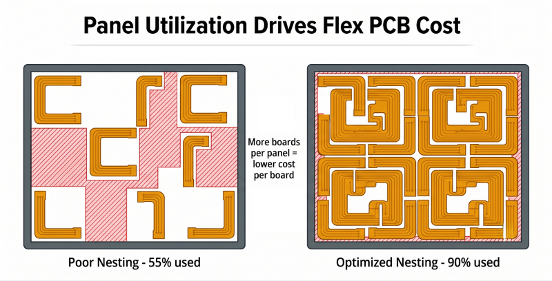
- Ask your fab for the panel size before finalizing the outline.
- Test a rotated or mirrored nest. Interlocking two orientations often gains a full row.
- Round the outline to panel-friendly dimensions. Trimming 2 mm off a width sometimes adds a whole column.
- Combine designs onto one panel when several small flex parts share a program.
- Keep the array conventions your fab expects, following standard panelization practice.
A 5 percent width reduction that adds one column per panel beats any material substitution.
Choose Cost-Effective Materials and Follow DFM Guidelines
Separate what the application needs from what merely sounds safer, then default to the cheaper option.
- 50 µm polyimide unless the bend demands 25 µm
- Adhesive-based laminate for static or one-time-bend designs
- 18 µm copper by default, 35 µm only where current demands it
- Yellow coverlay unless the product is visible to the end user
- 1 µin ENIG unless long storage or repeated reflow justifies 2 µin
- Polyimide stiffeners where FR4 is not structurally necessary
- Standard lead time, since rush production carries a real premium
Choosing a Cost-Effective Flex PCB Manufacturer
The cheapest quote and the lowest total cost are rarely from the same supplier. You are buying capability, yield, and the feedback that stops an expensive mistake.
Manufacturing Capability and Quality Control
The capability breadth determines if your design is drawn or value-engineered to a weaker form. Inquire about the number of layers, minimum trace and space per copper weight, and available stiffener materials. Quality control is more critical with flex, where defects are concealed – a microcrack in a bend area is not visible during QA, but is a fault in the field. Verify with visual inspection and flying probe test on each board, and inquire which IPC-6013 class the supplier builds to.
Material Options and Customization Support
A supplier with a narrow material menu will quietly push your design toward whatever they stock. Each option you cannot get becomes a compromise in your design or a second supplier to manage.
The most underrated cost factor is whether one supplier can carry you from five prototype boards to ten thousand. Switching vendors mid-program means requalifying the process, re-cutting tooling, and absorbing a new learning curve.
JLCPCB's Cost-Effective Flex PCB Manufacturing Capabilities
This is where a flex project either stays on budget or does not, and it comes down to matching your stackup to a fab's standard capability.
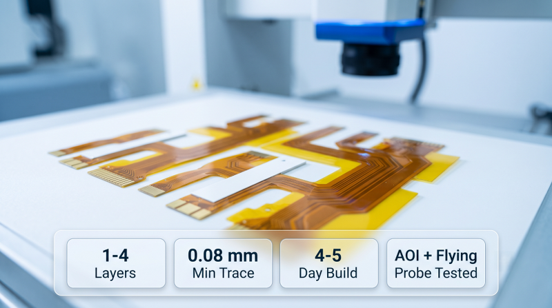
Advanced Manufacturing Technology for Reliable FPC Production
JLCPCB offers flexible PCB manufacturing in 1-layer, 2-layer, and 4-layer, with a minimum trace and space of 0.08 mm (3.15 mil). Each board goes out AOI and flying probe tested prior to shipping, and board sizes and profiling tolerances listed above are production board sizes and tolerances, not special order.
Flexible Material, Coverlay, and Stiffener Options
The menu includes polyimide at both typical dielectric thicknesses, adhesive-free substrate for dynamic bending, and transparent PET for 1 and 2-layer builds.
- Copper weights: 12 µm, 18 µm, and 35 µm
- Coverlay colors: yellow, black, white, and transparent
- Stiffeners, tapes, and EMI film: the full set listed in the stiffener table above
- Surface finish: ENIG at 1 µin or 2 µin
Professional DFM Analysis to Optimize Manufacturing Cost
Automated DFM analysis runs on your uploaded files and flags expensive problems before tooling is cut: coverlay openings tighter than the clearance rule, vias inside declared bend zones, and features below the trace-and-space limit for your copper weight. Catching one at the quote stage is usually worth more than the entire order value. The instant quote system returns price and DFM feedback together.
Support from Flex PCB Prototype to Production Manufacturing
Prototype and volume run on the same line with the same process, so there is no requalification step when quantities grow. SMT assembly is available for flex builds, with components drawn from the JLCPCB parts library. For a flex tail paired with a rigid motherboard, one supplier removes a shipping leg and a set of incoming inspections.
Conclusion
Flex PCB cost is not one number; it is a stack of decisions. Material area, layer count, quantity, feature difficulty, and finishing options each contribute a slice, and almost every expensive quote traces back to one or two of them.
Bare-board price is also the wrong benchmark. Flex earns its premium by deleting connectors, harnesses, labor, and failure points from the finished product, so a design that looks expensive on a quote sheet often ends up cheaper installed. Price two or three stackup variants through JLCPCB's instant quote before you commit.

Frequently Asked Questions About Flex PCB Cost
How Much Does a Flex PCB Cost?
Flex PCB pricing starts from around $25 for 5 pieces at a high-volume prototyper such as JLCPCB. Final cost depends on board size, layer count, quantity, and finishing options, so the only accurate figure is the one your own instant quote returns.
Why Are Flex PCBs More Expensive Than Rigid PCBs?
Polyimide film costs several times more per unit area than FR4, and flex adds process steps rigid boards do not have: coverlay cutting and registration, stiffener bonding, and laser profiling. Thin film also moves dimensionally during lamination, which lowers yield.
What Factors Affect Flexible PCB Pricing?
The main drivers are layer count, board area, and panel utilization, order quantity, copper weight, minimum feature size, and finishing options such as ENIG thickness, coverlay color, and stiffener material. Layer count is the most aggressive multiplier.
How Can I Reduce Flex PCB Manufacturing Costs?
Remove layers wherever routing allows, redraw the outline so more boards nest into each panel, and stay inside standard capability instead of specifying absolute limits. Review every finishing option individually, since stiffeners, thicker gold, and non-standard coverlay colors are frequently specified without a real requirement.
How Do I Get an Accurate Flex PCB Quote?
Upload your Gerber files to an instant quote tool and enter your real stackup: layer count, dielectric thickness, copper weight, coverlay, and stiffener zones. Quote two or three variants with one fewer layer or a smaller outline, because comparing them reveals which option carries most of your cost.

Popular Articles
• Understanding the Basics of Electronic Devices and Circuits
• Understanding Digital Circuit Timing: Setup Time, Hold Time, Contamination Delay & Clock Skew
• PCBs Explained: A Simple Guide to Printed Circuit Boards
• Guide to the Top 10 Commonly Used Electronic Components
• Digital 101: Fundamental Building Blocks of Digital Logic Design
Keep Learning
Demystifying Bare PCB Quality for Reliability-Critical Applications
Key Takeaways Early Defect Catching: Catching faults at the bare board stage costs only the PCB, avoiding wasted components and rework later. Perfboard Risks: Zero PCBs lack reference planes and plated holes, causing signal noise above 10–20 MHz and pad lifting. Critical Material Specs: Reliability depends on hole barrel copper (20–25 µm), Tg, Td, and CTI ratings matching your operating environment. Finish & Shelf Life: HASL and ENIG last ~12 months, while OSP and Immersion Silver/Tin expire in ~6 mon......
A Comprehensive Guide to Capacitor ESR: What It Is, Good Values, and How to Measure It
Key Takeaways Definition: Capacitor ESR (equivalent series resistance) is the single resistance that represents the losses inside a real capacitor, from its electrodes, terminations, electrolyte, and dielectric. Why It Matters: Ripple current flowing through the ESR produces a ripple-voltage step on the supply rail and I²R heating in the capacitor, which limits the capacitor's ripple-current rating and service life. Conditions Matter: ESR varies with frequency, temperature, capacitance, case size, and......
Understanding IPC-6012 Standards for High-Reliability Rigid PCB Fabrication
Key Takeaways IPC-6012 vs. IPC-A-600: IPC-6012 is the binding specification, while IPC-A-600 is only for visual reference. Class 2 vs. Class 3: Class 3 requires thicker copper (25μm vs. 20μm) and zero plating voids. Coupon Verification: Quality is tested by microsectioning panel coupons after thermal stress. Upfront Callout: Specify the class on drawings upfront; boards cannot be upgraded later. IPC-6012 is the line on your fabrication drawing that decides what your supplier is allowed to ship. Most d......
Mastering PCB Plating Types and Process Control in High-Yield Fabrication
Key Takeaways Two-Step Plating: Chemical seed layer comes first, electrolytic copper adds structural strength. Process Choice: Pattern plating enables fine tracks; panel plating suits heavy copper. Via Integrity: Keep aspect ratio ≤ 10:1 to prevent thinnest-point barrel cracking. Surface Finishes: Use ENIG for flat BGA pads and hard gold for high-wear contacts. IPC Standards: Class 2 mandates 20μm copper wall thickness; Class 3 requires 25μm with zero voids. PCB plating turns a stack of drilled lamina......
Can PCB Autorouters Really Deliver Production-Ready Designs?
Key Takeaways Rules over DRC: A clean DRC only proves rules were followed, not that the board works. Placement First: Autorouters cannot compensate for bad component placement. Selective Automation: Hand-route power, analog, and high-speed traces; autoroute only repetitive or low-speed nets. DFM Validation: Verify real manufacturing tolerances before sending files to production. Every PCB autorouter sells the same promise: press one button and watch the ratlines turn into copper. On a simple two-layer......
Basic Bridge Circuits
Key Takeaways Core Principle: Bridge circuits (Wheatstone, Kelvin, H-Bridge, etc.) enable high-precision measurements and power control. Applications: Essential for sensor signal conditioning, AC/DC rectifiers, and motor drivers. JLCPCB Optimization: Maximize circuit stability with JLCPCB’s 3/3 mil traces, 4-layer stackups, and High-TG FR-4. A bridge circuit splits an input voltage into two paths, compares the voltages across different branches, and provides an output. These circuits are widely valued......