
Why a Clean PCB Netlist Is the Foundation of Successful Manufacturing
11 min
- Essential Elements Every Professional Netlist Should Include
- Common Netlist Pitfalls and How to Avoid Them
- From Netlist to Reliable PCB Production
- JLCPCB's Strength in Netlist-Driven PCB Manufacturing
- FAQ about PCB Netlist
- Conclusion
Key Takeaways
A clean PCB netlist is the foundation of successful manufacturing, serving as the single source of truth that bridges schematic and physical PCB layout. By ensuring accurate component data, net connections, and version control, it prevents costly errors, improves yield, and enables reliable production. Mastering IPC-D-356 netlist best practices helps engineers reduce risks and achieve high-quality results with JLCPCB.
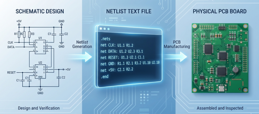
Ever wonder what exactly the link is between your wonderfully drawn schematic and the real copper traces on the fabricated board? It's the PCB netlist, a simple text file that contains all the electrical blueprint of your design. Otherwise, the schematic only carries a picture of what you are designing, and the layout will only be geometry.
There is one source of truth for each electrical connection in your circuit: a netlist. It is used to inform the layout tool about what pins are connected to which nets, what components exist, and how they are related. In this article, we will explore the meaning of a netlist, what should be included in a netlist, and some of the common mistakes that even seasoned engineers can make when working with netlists.
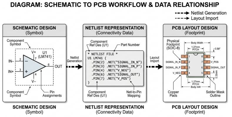
The Bridge Between Schematic Design and Physical Layout
Basically, the PCB netlist is an ASCII text file that contains all the electrical connections of your circuit, but omits the graphic data. Consider it an abstraction level. Your schematic is a design intent consisting of symbols and wires. Your PCB layout includes physical reality in the form of pads, traces, and vias. The netlist is how these two worlds are connected.
Once finished with your schematic in an EDA (EasyEDA, KiCad, or Altium Designer), the EDA software will generate a netlist that includes all the connectivity information. The netlist can be either flat or hierarchical. A flat netlist is the most common type of netlist in PCB workflows, where all connections are listed without any groups. A hierarchical netlist is a netlist that keeps the structure of a multi-sheet schematic by collecting nets in groups, defined by their parent sheet. Most of the EDA tools support both of these, and the choice is based on the complexity of the design and the team workflow.
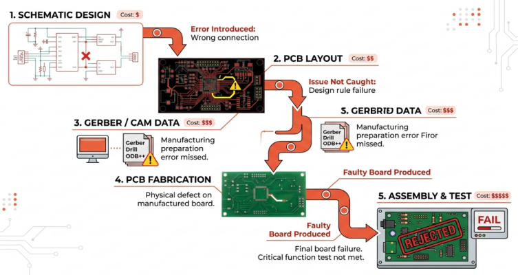
How Netlist Errors Can Cascade into Production Problems
Let's get the bad news out of the way. The one netlist error does not cause one error, but cascades. A net that is not in the netlist will never be offered to be routed by the layout tool. That unrouted connection then passes DRC (not part of anything to check), Gerber generation, CAM processing, and only comes to light when the assembled board fails to work.
The more time that passes, the more expensive it is to fix the error:
- Schematic stage: A few minutes to fix a wire or net label
- Layout stage: time depending on routing density.
- Gerber/CAM stage: (with re-review fees if applicable)
- Fabrication stage: Days of wasted production time and materials should be eliminated.
- Assembly and test stage: Full rework or board re-spin, hundreds to thousands of dollars.
A netlist is a text file that contains all the essential elements needed by every professional netlist.
Essential Elements Every Professional Netlist Should Include
Accurate Component Data, Net Connections, and Attributes
For each component in your netlist, you must provide the following information:
- Reference designator: unique identifier for each component instance
- Value of component: the electrical value/part number
- Footprint: physical land pattern for layout
- Attributes: Other information, including tolerance, voltage rating, manufacturer part number, or DNP (Do Not Populate) status
Net entries should contain a unique net name and a list of all pins that are part of the net. Of course, there are a number of nets that are particularly noteworthy, such as power nets like VCC, GND, 3V3, and 5V, which are generally connected to dozens or hundreds of pins. When a power net is not complete, it can be deadly.
A summary of the critical data elements and their roles is given below:
| Netlist Element | Example | Role in Manufacturing |
|---|---|---|
| Reference Designator | U3 | Identifies component placement on BOM and CPL files |
| Component Value | STM32F103 | Ensures the correct part is sourced and placed |
| Footprint | LQFP-48 | Determines pad geometry and stencil aperture design |
| Net Name | SPI_CLK | Guides routing and enables electrical test verification |
| Pin Mapping | U3.Pin14 = SPI_CLK | Ensures correct pin-level connectivity in layout |
| Attributes | DNP, 50V rating | Drives assembly instructions and BOM filtering |
Best Practices for Version Control and Documentation
Netlist management is not a one-shot. Designs change, and each schematic change results in a new netlist. If you don't keep track of your versions, you could be sending an old netlist for layout or even worse, to fabrication.
To ensure a strong netlist workflow, do the following:
- Regenerate the netlist after any schematic change, regardless of the magnitude of the change. If the netlist is stale, the names don't match even if you change the net label name.
- Maintain a synchronic schematic and layout with the built-in annotation and back-annotation functions of your EDA tool. When configured properly, tools such as EasyEDA and KiCad will do this automatically.
- Use version control for netlists (git, svn, date-stamped file system, etc.). This will let you compare changes to previous revisions and prevent unwanted changes.
- Record the team's net naming conventions. No confusion and fewer merge conflicts in collaborative designs (e.g., SPI_MOSI, UART1_TX, PWR_5V).
- Add a netlist revision log that documents changes, when, and why. This is particularly crucial when passing along designs to a manufacturing partner.
Common Netlist Pitfalls and How to Avoid Them
Duplicate Nets, Missing Connections, and Naming Issues
The most frequent netlist errors fall into a few well-known categories:
- Duplicate net names: Two electrically separate nets are named the same. This causes the layout tool to short them together and cause a functional failure, which may not be apparent on review.
- Unconnected pins: A pin that is supposed to connect to a net is not connected in the schematic. Either it will not be included in the netlist, or it will be assigned to an unnamed net, which will create issues downstream.
- Missing components: A component is shown in the schematic but has been improperly annotated, which means there is no reference designator. The netlist might ignore it, or a netlist might contain a netlist that the layout tool cannot resolve.
- Errors with pin swaps: Two pins of a multi-function IC are accidentally swapped in the schematic symbol. The netlist accurately reflects the incorrect mapping, and this error goes unnoticed during layout and manufacturing.
From Netlist to Reliable PCB Production
Seamless Handover to DFM and Fabrication Stages
Netlist is the reference standard for electrical verification at fabrication. It is used by manufacturers for bare-board electrical testing (usually with flying probe or bed-of-nails fixtures) per IPC-9252. If you don't have a valid IPC-D-356 netlist, then the fabricator won't be able to ensure that each connection on the board they're making is the one you intended.
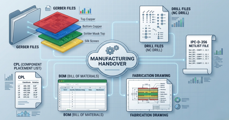
A manufacturing “handover” package should contain:
- Gerber files of all layers (Or ODB++ / IPC-2581 format)
- Drill files (Excellon format) and Tool table
- IPC-D-356A netlist of electrical test
- Fabrication Drawing including Stackup, Material, and Finish Specification
- BOM and CPL (Component Placement List) files for assembly.
- Special instructions/constraints
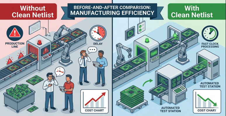
How Accurate Netlists Improve Yield and Reduce Revisions
The more quality design data is provided, the more the manufacturing yield is affected. A clean netlist helps improve yield in a number of ways:
| Netlist Quality Factor | Impact on Manufacturing |
|---|---|
| All nets are correctly defined | Electrical test catches 100% of open/short defects |
| Consistent net naming | Reduces CAM processing errors and review time |
| Complete pin mapping | Ensures no connections are missed during routing verification |
| Matched BOM/netlist data | Prevents wrong-component placement during assembly |
| IPC-D-356 included | Enables automated bare-board testing, catching defects before assembly |
Clean netlist boards tend to have fewer engineering queries (EQs) during fabrication, lower test escapes, and lower first article failures. Even a small yield increase can be important in high-volume production. The mathematics is simple. On a 10K board production run at $5 per board, a netlist error that results in a 2% yield loss translates to $1K in material waste, not to mention the labor that has to be invested in root cause analysis and corrective action. The netlist review is a 30-minute activity that removes that risk completely.
JLCPCB's Strength in Netlist-Driven PCB Manufacturing
Thorough DFM Review Based on Clean Netlists
JLCPCB does a thorough DFM check for each order prior to manufacturing. This review is not a standard Gerber inspection. By submitting an IPC-D-356 netlist along with your order, you enable JLCPCB's engineering team to cross-validate the connectivity that was extracted from your Gerber files with your design intent, helping to identify discrepancies that might not be spotted during visual Gerber inspection. It is especially easy to integrate for designers who use EasyEDA. EasyEDA outputs all the required manufacturing files (such as netlist) in the format optimized for JLCPCB's production process. The close relationship between the design tool and the manufacturer minimizes the likelihood of file format mismatches and conversion errors.
Consistent High-Quality Results Across All Production Volumes
From an initial order of 5 prototype boards at $2 to a production run of 10,000 pieces, JLCPCB always maintains the same quality standards. Standard boards can turn around as quickly as 1-2 days, so even if a netlist problem is identified during the DFM review, the corrected file can be turned around quickly. In the assembly order, the netlist-BOM-CPL alignment is cross-checked during the SMT assembly process, so that the component placement is in accordance with your design. This is an end-to-end verification, from netlist to final assembly.
FAQ about PCB Netlist
Q: What is a netlist in PCB design?
A PCB netlist is a text-based file that describes every electrical connection in your circuit. It lists all components (with reference designators, values, and footprints) and all nets (with the pins that belong to each net). The netlist serves as the bridge between your schematic and your physical PCB layout.
Q: What format should my netlist be in for manufacturing?
For bare-board electrical testing, the standard format is IPC-D-356A. For design transfer between EDA tools, common formats include EDIF and proprietary formats specific to each tool (such as KiCad's .net or Altium's .NET). For simulation, SPICE netlists are the standard. Always check with your manufacturer for preferred formats.
Q: Can I manufacture a PCB without a netlist?
Technically, a manufacturer can fabricate a board from Gerber files alone. However, without an IPC-D-356 netlist, the fabricator cannot perform electrical testing to verify connectivity. This means open or short defects may go undetected until assembly or functional testing, significantly increasing your risk.
Q: How do I verify my netlist before sending it to manufacturing?
Run your EDA tool's Electrical Rules Check (ERC), perform a netlist diff against previous versions, cross-reference against your BOM, and manually inspect critical power and ground nets. For final verification, use a CAM tool to compare the extracted Gerber connectivity against your IPC-D-356 netlist.
Conclusion
A clean and accurate PCB netlist is far more than just an intermediate file — it is the electrical DNA of your entire design and the cornerstone of successful PCB manufacturing. From schematic capture to final assembly, the netlist serves as the single source of truth that ensures every connection, component, and intention is faithfully translated from digital design into physical reality.
By maintaining a high-quality netlist, engineers can dramatically reduce costly errors, accelerate design iterations, improve manufacturing yield, and minimize the risk of board re-spins. Whether you are building a quick prototype or preparing for high-volume production, investing time in netlist verification, proper version control, and adherence to best practices will pay significant dividends in reliability and time-to-market.
JLCPCB supports this rigorous approach by offering comprehensive DFM reviews and advanced electrical testing capabilities when a clean IPC-D-356 netlist is provided. In today’s fast-paced electronics industry, those who master the netlist are those who consistently deliver working boards on time and within budget.
Popular Articles
• Understanding Electrical Schematics: A Comprehensive Guide
• The Comprehensive Guide to Circuit Symbols: Key to Understanding Electrical and Electronic Diagrams
• PCB Board Design: A Step-by-Step Guide for Beginners
• Choosing the Best PCB Color-Enhancing Aesthetics and Functionality
• PCB Silkscreen: All You Need to Know
Keep Learning
Understanding Electrical Schematics: A Comprehensive Guide
Key Takeaways Schematics vs. Block Diagrams: Schematics detail exact components and connections; block diagrams only show high-level functions. Mark Polarity: Essential to prevent circuit failure and automated SMT placement errors at JLCPCB. Clean Layout: Use modular blocks and net labels (VIN, GND) to eliminate visual clutter. Manufacturing Ready: Follow DFM trace rules and export standard Gerber, BOM (LCSC C-IDs), and CPL files. Fast Troubleshooting: Isolate schematic blocks to test expected voltage......
A Beginner's Guide to Basic Electronic Components: Functions, Symbols & Uses
Every circuit, from a simple LED flashlight to a microcontroller board, is built from the same handful of common electronic components. This guide breaks down the ten basic electronic components you will encounter most often: What each component does How it works Key specifications Where engineers use it By the end, you will be able to recognize these electronic circuit components on a schematic, a PCB, or a parts bin, and know exactly why each one is there. These electronic components are the buildin......
Via Stubs in High-Speed PCB Design: Causes, Effects, and Solutions
Key Takeaways Via stubs are unused via sections that cause reflections, resonance, and jitter in high-speed PCBs. They become critical above 5–10 Gbps; stubs longer than 15 mils (0.381 mm) need mitigation. JLCPCB precision back-drilling reduces residual stubs to under 0.15 mm, greatly improving signal integrity. Optimized stack-up and back-drilling offer the best balance of performance and cost versus blind/buried vias. Choose experienced manufacturers like JLCPCB for reliable high-speed PCB fabricati......
The Comprehensive Guide to Circuit Symbols: Key to Understanding Electrical and Electronic Diagrams
Note Need a quick reference while reading schematics? Download our free, printable Circuit Symbols Cheat Sheet (PDF), featuring the most common IEC and ANSI symbols organized by category. Keep it on your desktop or print it for easy reference at your workbench. ⬇ Download the Free Circuit Symbols Cheat Sheet (PDF) Every electronic diagram is written in a visual language, and circuit symbols are its alphabet. From your first electrical schematic to a multi-layer board, knowing circuit symbols can make ......
Hierarchical Design : Making Complex PCB Projects More Manageable
Key Takeaway Hierarchical design transforms complex PCB projects from overwhelming single-sheet nightmares into well-organized, modular, and manageable systems. By breaking down large schematics into functional blocks with clear interfaces, engineers can significantly improve organization, reduce errors, enhance reusability, and enable smoother collaboration. This approach not only simplifies debugging and layout but also leads to better DFM outcomes and faster time-to-market, making it the preferred ......
Why a Clean PCB Netlist Is the Foundation of Successful Manufacturing
Key Takeaways A clean PCB netlist is the foundation of successful manufacturing, serving as the single source of truth that bridges schematic and physical PCB layout. By ensuring accurate component data, net connections, and version control, it prevents costly errors, improves yield, and enables reliable production. Mastering IPC-D-356 netlist best practices helps engineers reduce risks and achieve high-quality results with JLCPCB. Ever wonder what exactly the link is between your wonderfully drawn sc......