Via Stubs in High-Speed PCB Design: Causes, Effects, and Solutions
13 min
- What Is a Via Stub and Why It Matters in Modern Electronics
- How Via Stubs Are Formed and Their Negative Effects on Signal Integrity
- Effective Strategies to Minimize or Eliminate Via Stubs
- JLCPCB's Professional Capabilities in Via Stub Control and High-Speed PCB Manufacturing
- FAQ about Via Stubs in High-Speed PCB Design
- Conclusion on Via Stubs in High-Speed PCB Design
Key Takeaways
- Via stubs are unused via sections that cause reflections, resonance, and jitter in high-speed PCBs.
- They become critical above 5–10 Gbps; stubs longer than 15 mils (0.381 mm) need mitigation.
- JLCPCB precision back-drilling reduces residual stubs to under 0.15 mm, greatly improving signal integrity.
- Optimized stack-up and back-drilling offer the best balance of performance and cost versus blind/buried vias.
- Choose experienced manufacturers like JLCPCB for reliable high-speed PCB fabrication with strict via control.
In high-speed PCB designs, a via stub — the unused portion of a plated through-hole via — creates significant signal integrity challenges. As data rates climb beyond 5–10 Gbps, these stubs introduce reflections, resonances, and jitter that can close eye diagrams and increase bit error rates. Understanding via stubs, their formation, and effective mitigation strategies helps engineers deliver reliable performance. Manufacturers like JLCPCB provide practical solutions such as precision back-drilling on multilayer boards up to 32 layers.
What Is a Via Stub and Why It Matters in Modern Electronics
A via stub refers to the unused segment of a through-hole via that extends beyond the last connected signal layer. In a multilayer PCB, a signal transitioning from Layer 1 to Layer 3 leaves the copper barrel from Layer 4 to the bottom as a stub. This acts as an open transmission line stub, creating parasitic inductance and capacitance.
Via stubs matter because modern systems — 5G base stations, automotive radar, data center switches, and high-performance computing — operate at frequencies where even short stubs become problematic. A stub longer than 15 mils (0.381 mm) often requires mitigation on boards thicker than 1.2 mm. JLCPCB's capabilities in controlled-depth drilling address these issues directly for volume production.
Engineers can no longer treat vias as simple interconnects. At multi-gigabit speeds, every discontinuity affects the channel budget.
Basic Definition of PCB Vias and Via Stubs
A standard via is a drilled and plated hole that electrically connects traces on different layers. When the via extends fully through the board but the signal only uses part of it, the remaining plated barrel becomes a via stub.
This stub behaves like a resonant stub antenna at high frequencies. Its electrical length depends on physical length, dielectric constant (typically 4.0–4.5 for FR-4), and frequency. Stubs create impedance discontinuities, leading to signal reflection and potential system-level failures in severe cases.
In practice, designers encounter stubs most often in thick, high-layer-count boards where through-hole vias are the most cost-effective choice for many nets.
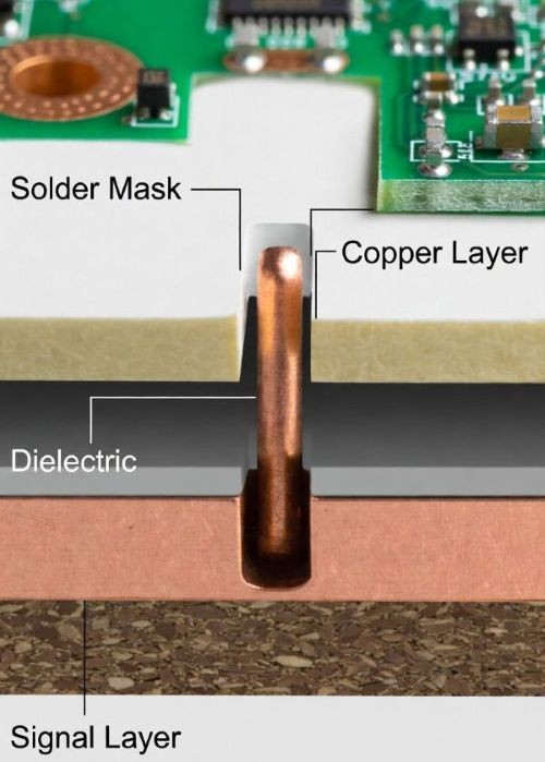
Visual comparison of through-hole vias, blind vias, buried vias, and how via stubs form in standard through-hole designs.
The Difference Between Through-Hole Vias, Blind Vias, Buried Vias, and Stubs
Through-hole vias span the entire board thickness. They are easy to manufacture but create the longest potential stubs.
Blind vias connect an outer layer to an inner layer without penetrating the full board. Buried vias connect only internal layers and require sequential lamination. A via stub is specifically the non-functional extension on any via type, though most common with through-hole designs.
Blind and buried vias eliminate stubs by design but increase fabrication steps and cost. Back-drilling a through-hole via often provides comparable electrical performance at lower overall expense. JLCPCB supports standard through vias with back-drilling on 4–32 layer boards, balancing density, performance, and manufacturability.
When Via Stubs Become Critical: High-Speed Signals, 5G, Automotive, and Data Centers
Via stubs become critical above 5–10 Gbps or when board thickness forces stub lengths over 15 mils. In 5G infrastructure, a stub resonance near the Nyquist frequency can degrade return loss dramatically. Automotive radar modules operating at 24/77 GHz are especially sensitive to any additional radiation or loss. Data center ASICs handling 112G PAM4 or higher demand extremely clean channels with minimal jitter.
Real deployments show that unmitigated stubs force designers to add heavy equalization or shorten trace lengths, raising power consumption and system complexity. JLCPCB's back-drilling process helps maintain performance using standard stack-ups.
How Via Stubs Are Formed and Their Negative Effects on Signal Integrity
Via stubs form naturally during standard multilayer fabrication. After drilling and plating a through-hole, any portion beyond the functional signal layers remains as a conductive stub. The longer the board or the deeper the transition, the longer the potential stub.
These stubs introduce parasitic effects that scale with frequency and length. In high-speed channels, they are often the dominant source of discontinuity.
The Physics Behind Stub Resonance and Impedance Discontinuity
A via stub acts as an open-circuited transmission line. Its input impedance varies with frequency and creates reflections when it deviates from the trace impedance (typically 50 Ω single-ended or 100 Ω differential).
The quarter-wavelength resonance frequency can be estimated as:
f ≈ c / (4 × L_stub × √ε_r)where c is the speed of light, L_stub is stub length, and ε_r is the dielectric constant. For a 0.5 mm stub in FR-4 (ε_r ≈ 4.3), resonance appears around 10–12 GHz — right in the operating band for many 25 Gbps signals.
This resonance produces a sharp notch in insertion loss (S21) and a peak in return loss (S11). Parasitic capacitance is roughly 0.5–1 pF per mm of stub length, while inductance adds 0.3–0.5 nH per mm.
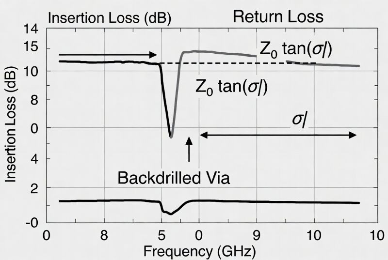
Signal integrity degradation caused by via stubs, showing reflections, insertion loss notches, and increased crosstalk in high-speed differential pairs.
Common Problems: Reflections, Insertion Loss, Crosstalk, and Bit Error Rates
Reflections from a via stub cause ringing and inter-symbol interference (ISI). Insertion loss increases due to energy diverted into the stub. In differential pairs, even small stub length mismatch between P and N creates skew of 0.5–1 ps per 0.1 mm difference, harming timing margins in DDR5 or Ethernet.
Crosstalk rises because the stub radiates into adjacent vias and reference planes. The net result is higher jitter, reduced eye height, and elevated bit error rates. In extreme cases, a system may fail compliance testing entirely.
Table 1: Typical Performance Impact of Via Stubs (10-layer board, ~1.6 mm thick, 0.2 mm via)
| Metric | With ~0.5 mm Stub | Backdrilled (<0.15 mm) | Improvement |
|---|---|---|---|
| Return Loss @ 5 GHz | –12 dB | –22 dB | +10 dB |
| Insertion Loss @ 5 GHz | –3.5 dB | –1.8 dB | 1.7 dB better |
| Peak-to-Peak Jitter | 18 ps | 9 ps | 50% reduction |
| Eye Height | 0.55 UI | 0.78 UI | +42% |
| Resonance | ~11 GHz | Eliminated in band | None |
Real-World Case Studies of Via Stub Failures in High-Frequency Designs
One 12-layer 25 Gbps networking board initially failed PCIe compliance due to excessive jitter on critical differential pairs. Cross-section analysis revealed stubs averaging 0.6 mm. After implementing back-drilling, eye height improved by approximately 40% and the board passed testing.
In a 5G mmWave module, unmitigated stubs caused return loss notches exceeding 8 dB, forcing extra equalization and increasing power draw. Switching to controlled-depth drilling eliminated the notches and simplified the receiver design. These examples illustrate why fabricators like JLCPCB integrate back-drilling into standard multilayer workflows.
Effective Strategies to Minimize or Eliminate Via Stubs
Designers have several proven methods to control via stubs. The choice depends on frequency, layer count, cost targets, and density requirements.
Back-Drilling (Backdrill) Technology – Principles and Advantages
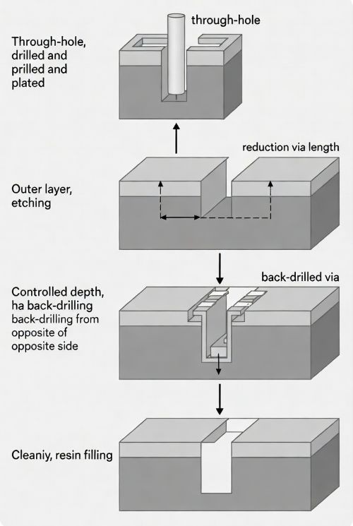
Back-drilling removes the unused copper barrel with a second, larger-diameter controlled-depth drill from the opposite side of the board after initial plating. JLCPCB's process targets residual stubs below 0.15 mm (6 mils), well under the 15 mil (0.381 mm) threshold where resonance becomes problematic.
- Maintains simple stack-ups compared to blind/buried vias
- Improves return loss, insertion loss, and eye diagrams with modest added cost (typically 5–10% for high-layer boards)
- Compatible with standard FR-4 and high-frequency materials
The process uses high-RPM CNC equipment with laser depth control (±0.05 mm accuracy) and vision alignment. Debris is removed via vacuum and ultrasonic cleaning, followed by resin filling. JLCPCB supports this on boards from 4 to 32 layers.
Blind and buried via structures in a multilayer PCB, showing how these via types eliminate stubs by avoiding unused barrel extensions.
Blind and Buried Vias: When to Use Them in Multilayer PCBs
Blind vias connect outer to inner layers; buried vias connect only internal layers. Both eliminate stubs by design but require additional lamination cycles and laser drilling for microvias. They excel in ultra-high-density BGA fan-out regions or when back-drilling clearance cannot be guaranteed.
For many long-haul signals, back-drilling a through via offers nearly equivalent performance at lower cost and faster turnaround. A hybrid approach — back-drilled through vias for most routing and micro blind vias for dense areas — is common in JLCPCB high-speed builds.
Optimized Layer Stackup Design and Via Placement Best Practices
Careful stack-up planning minimizes stub lengths from the start. Place high-speed signals on layers close to the surface or reference planes to reduce via travel distance. Use ground vias around signal vias for better return paths and reduced crosstalk.
Design Tip
JLCPCB recommends enlarging antipads on unused layers by 0.1 mm when back-drilling to ensure clearance. Via placement should avoid dense clusters that complicate depth control. Simulation of the full channel, including via models, remains essential before tape-out.
Advanced Techniques: Skip Vias, Microvias, and Filled Vias
Skip vias jump multiple layers with controlled depth. Microvias (laser-drilled, typically <0.15 mm) suit HDI designs and can be stacked or staggered. Filled vias (with conductive or non-conductive fill) improve thermal performance and allow via-in-pad, though back-drilling compatibility needs verification to avoid solder wicking.
These techniques complement back-drilling. JLCPCB's capabilities include microvia technology alongside precision back-drilling for complex high-speed boards.
JLCPCB's Professional Capabilities in Via Stub Control and High-Speed PCB Manufacturing
JLCPCB integrates via stub mitigation into its standard production flow, supporting engineers from prototype to volume without forcing expensive process changes.
1Precision Back-Drilling Services with Tight Depth Control
JLCPCB's back-drilling uses CNC machines with closed-loop servo and laser interferometry for depth accuracy of ±0.05 mm. The process occurs after outer-layer etching but before solder mask. Residual stubs are controlled to <0.15 mm, with test coupons cross-sectioned for verification on every panel.
Designers specify back-drill layers via separate drill files or diameter differentiation (e.g., +0.1 mm larger for back-drilled holes). This ensures clean, repeatable results across 4–32 layer boards.
2Advanced Multilayer Fabrication up to 32 Layers with Microvia Technology
JLCPCB fabricates multilayer PCBs up to 32 layers in standard offerings, with controlled impedance across the full range. Microvia and HDI options support higher densities where needed. Back-drilling works alongside these processes, giving designers flexibility without compromising lead times.
3High-Frequency Material Expertise and Impedance Control Excellence
The manufacturer works with FR-4, Rogers, and PTFE materials, maintaining ±10% impedance tolerance. DFM checks automatically flag vias likely needing back-drilling based on the 15-mil rule. Online impedance calculators and detailed reports help designers achieve consistent results.
4Quality Assurance: Testing, Verification, and Reliability for Stub-Free Designs
Every order includes rigorous checks: AOI, flying-probe electrical test, TDR/VNA validation on coupons, and cross-section analysis. Depth tolerance is tracked panel-wide. This ISO-certified process delivers repeatable stub control from prototypes through mass production, giving engineers confidence in high-speed deployments.
FAQ about Via Stubs in High-Speed PCB Design
Q: What exactly is a via stub and when does it become a problem?
A via stub is the unused plated barrel portion of a through-hole via that extends beyond the last connected signal layer. It becomes problematic above 5–10 Gbps data rates or when the stub length exceeds 15 mils (0.381 mm). At these frequencies, the stub behaves as a resonant antenna, creating impedance discontinuities that degrade signal integrity.
Q: How does back-drilling eliminate via stubs?
Back-drilling uses a second, larger-diameter controlled-depth drill to remove the unused copper barrel from the opposite side of the board after initial plating. This reduces the residual stub to below 0.15 mm (6 mils), well under the threshold where quarter-wavelength resonance causes significant signal degradation. The process uses CNC equipment with laser depth control for ±0.05 mm accuracy.
Q: What is the maximum acceptable via stub length for high-speed designs?
The commonly accepted rule is 15 mils (0.381 mm) as the threshold where back-drilling or stub mitigation should be considered. However, for very high frequencies (25 Gbps and above), even shorter stubs can cause issues. The actual limit depends on the signal frequency, board dielectric constant, and channel loss budget. For a 0.5 mm stub in FR-4, resonance appears around 10–12 GHz, which falls within the operating band of many 25 Gbps signals.
Q: Are blind and buried vias a better solution than back-drilling?
Blind and buried vias eliminate stubs by design since they don't extend through the full board thickness. However, they require additional lamination cycles and laser drilling, increasing fabrication cost and complexity. For many applications, back-drilled through-hole vias provide comparable electrical performance at lower cost. A hybrid approach — using back-drilled through vias for most routing and microvias only in dense BGA areas — often delivers the best balance.
Q: How does JLCPCB verify back-drilling quality?
JLCPCB verifies back-drilling quality through multiple inspection methods on every panel: AOI (Automated Optical Inspection), flying-probe electrical testing, TDR/VNA validation on test coupons, and cross-section analysis. Depth tolerance is tracked panel-wide under an ISO-certified process, ensuring consistent stub control from prototypes through volume production.
Conclusion on Via Stubs in High-Speed PCB Design
In summary, via stubs remain a key consideration in high-speed PCB design, but proven manufacturing techniques effectively control them. By combining good layout practices with precision fabrication capabilities like JLCPCB's back-drilling, engineers can achieve clean signals, open eye diagrams, and reliable system performance without unnecessary complexity or cost.
Popular Articles
• The Comprehensive Guide to Circuit Symbols: Key to Understanding Electrical and Electronic Diagrams
• Design Guidelines for PCB Using FR4 Substrates
• Choosing the Best PCB Color-Enhancing Aesthetics and Functionality
• PCB Silkscreen: All You Need to Know
• PCB Board Design: A Step-by-Step Guide for Beginners
Keep Learning
How to Read and Create PCB Schematics
Key Takeaways Read Schematics: Understand symbols, net labels, and component values. Design in EasyEDA: Place components and create circuit connections. Run Design Checks: Use ERC and DRC to identify potential issues. Verify Components: Check pin assignments and PCB footprints. Prepare for Manufacturing: Validate PCB layouts and manufacturing files. Printed circuit board (PCB) design begins with a clear understanding of how the electronic circuit should function. A schematic diagram represents the cir......
Maximizing Circuit Reliability with PCB Test Points and Smart DFT
Key Takeaways Early Fault Catching: Test points drastically reduce diagnosis time and prevent costly field failures. Standard Pad Sizing: Use 1.0 mm flat copper pads with 2.54 mm spacing for optimal fixture contact. Protect High-Speed Signals: Keep branch traces short to prevent capacitive loading and resonance. Single-Sided Access: Place all test pads on the bottom layer to cut fixture costs. Right Test for Volume: Use flying probe for prototypes and bed-of-nails ICT for mass production. A PCB test p......
The Comprehensive Guide to Circuit Symbols: Key to Understanding Electrical and Electronic Diagrams
Note Need a quick reference while reading schematics? Download our free, printable Circuit Symbols Cheat Sheet (PDF), featuring the most common IEC and ANSI symbols organized by category. Keep it on your desktop or print it for easy reference at your workbench. ⬇ Download the Free Circuit Symbols Cheat Sheet (PDF) Every electronic diagram is written in a visual language, and circuit symbols are its alphabet. From your first electrical schematic to a multi-layer board, knowing circuit symbols can make ......
Design Guidelines for PCB Using FR4 Substrates
Material substrate concerns are necessary while designing electrical circuit boards. This is due to the fact that printed circuit boards cannot be manufactured without the appropriate PCB materials. When developing and producing circuit boards, the substrate material must be taken into account just as much as the copper layers, silkscreen, and surface polish. Generally speaking, non-conductive materials like porcelain, Marlon, FR4, and the like must be used for PCB substrates. Depending on its intende......
Choosing the Best PCB Color-Enhancing Aesthetics and Functionality
Key Takeaways Choosing the best PCB solder mask color involves balancing aesthetics, visibility, and functionality. Green remains the top choice for superior contrast and inspection, while black offers premium appeal, white excels in LED applications, and other colors like purple and red provide unique design options. The ideal color depends on your priorities in inspection ease, thermal performance, and brand image, with minimal impact on electrical performance when using proper silkscreen contrast. ......
4 Layer vs 6 Layer vs 8 Layer PCB: How to Choose the Right Stackup
Random selection of layers in electronics may lead to serious signal integrity issues. That's why we always design our stackup before designing the PCB. Stackup decides the type of PCB and how it gonna perform under high-frequency conditions. There are a lot of things that directly affect the stackup of the PCB, related to impedance matching, routing density, signal and power integrity, electromagnetic compatibility (EMC), and cost. Knowing the requirements before design and the most critical componen......