
The Foundation of Every Great PCB: Mastering Schematic Capture
13 min
- Why Schematic Capture Is the Most Critical First Step
- Choosing the Right Schematic Capture Software and Tools
- Best Practices for Creating High-Quality Schematics
- Connecting Schematic Capture to Successful PCB Layout
- How Professional Schematic Capture Drives Manufacturing Excellence
- Frequently Asked Questions (FAQ)
Schematic capture is the process of creating an electronic circuit diagram using specialized software. Here we have to place component symbols (such as resistors, capacitors, ICs, and connectors) and connect them with wires to represent the electrical connection. Although it is not the real connection yet, but can be translated once it goes to layout. Hence, we can say on a big scale schematic capturing serves as the first step in the PCB design workflow, which allows designers to define how components interact electrically before moving to the physical PCB layout.
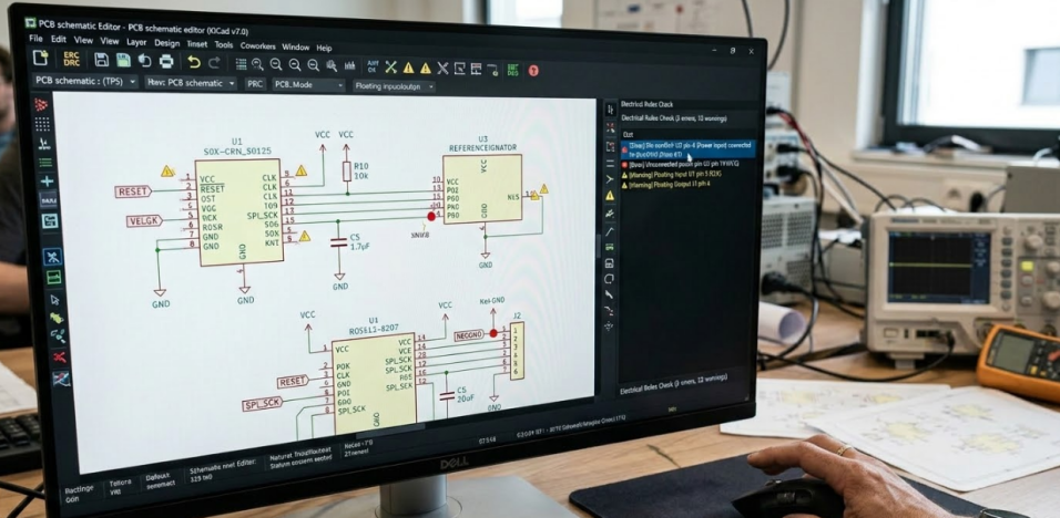
Schematic capture tools also help generate netlists, perform electrical rule checks (ERC), and prepare the design for further next stage. We are taking the example of a dense microcontroller board like the WCH32V003 and will see how the quality of your schematic determines the quality of your final product. Today, we will see how to choose the right tools and what will be the best practices that separate clean designs from messy ones.
Why Schematic Capture Is the Most Critical First Step
How a Well-Captured Schematic Impacts Final PCB Quality
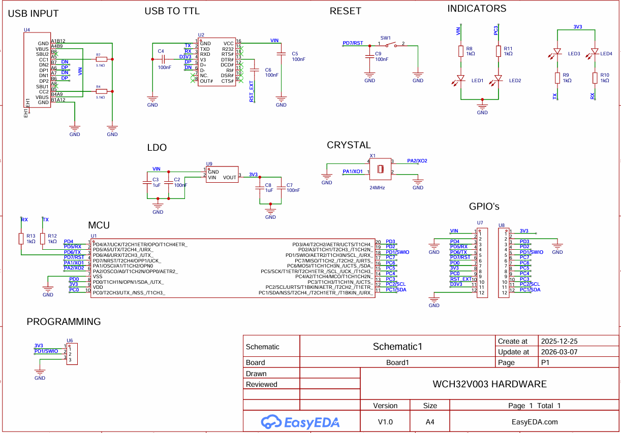
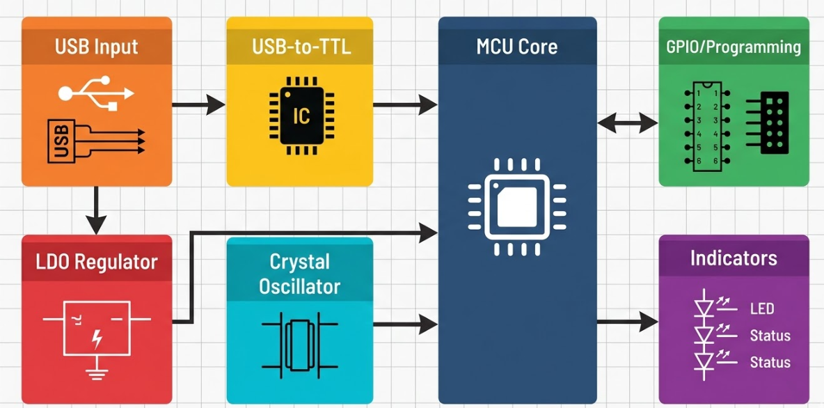
Think of your schematic as the architectural blueprint for your PCB. Just as a building architect organizes spaces by function, kitchen, bedrooms, utilities a well-structured schematic partitions the circuit into logical functional blocks. On the WCH32V003 board, these blocks are clearly defined: USB Input, USB-to-TTL, LDO, Crystal, MCU, GPIOs, Programming, Reset, and Indicators.
This clean block partitioning is not just about visual organization. It directly reduces layout mistakes. When your USB input section feeds cleanly into the LDO regulation stage, which then powers the MCU core and its peripherals, the signal flow is obvious to anyone reading the design.
Clear net naming is equally critical. On the CH32V003 board, programming and IO nets like PD1/SWIO, PD7/NRST, UART TX/RX, and I2C lines are labeled explicitly in the schematic. This prevents confusion during assembly, testing, and firmware bring-up. When a test engineer needs to probe the programming interface, there is no ambiguity about which pad carries SWIO versus which is a generic GPIO.
Common Pitfalls When Schematic Capture Is Rushed or Poorly Done
The most expensive mistakes in PCB design rarely originate in the layout tool. They originate in a sloppy schematic. Here are the pitfalls that cause the most downstream pain:
1.Missing power intent. When decoupling capacitors are not explicitly tied to the correct rails, you end up debugging voltage rail issues during bring-up. On a board with an LDO stage, this can mean the difference between a clean 3.3V output and a noisy unstable supply.
2.Ambiguous connector pin mapping. USB-C connectors carry configuration channel pins (CC1, CC2) alongside data lines (D+, D-) and power (VBUS). If these are not mapped precisely in the schematic, the board will fail during initial bring-up.
3.Inconsistent designators and net labels. If R12 in the schematic becomes R13 in the BOM, or if a net called UART_TX in one sheet appears as TX in another, the assembly house receives conflicting information. This breaks downstream BOM, CPL file generation, and assembly communication.
4.Floating pins left unaddressed. Unconnected MCU pins that are not explicitly marked as no-connect create ERC warnings that designers learn to ignore. But those warnings can mask real connectivity issues hiding underneath.
Choosing the Right Schematic Capture Software and Tools
Popular Professional Tools and Their Key Features
The schematic capture tool you choose shapes your entire design workflow. Here is a practical comparison of three popular options:
| Feature | Altium Designer | KiCad | EasyEDA |
| License Model | Commercial (subscription) | Open-source (free) | Free (web-based) |
| ERC Capability | Advanced rule-driven | Mature with configurable rules | Built-in with quick checks |
| Schematic-to-PCB Sync | Tight bidirectional sync | Forward/back annotation | Integrated single-environment |
| BOM Generation | Native with variants | Plugin-based and built-in | Direct export with part linking |
| Library Ecosystem | Manufacturer Part Search | Community + official libs | LCSC-integrated parts library |
| Learning Curve | Steep | Moderate | Low |
Altium Designer offers the most integrated rule-driven flow with tight schematic-to-PCB synchronization. It is the standard in many professional teams where complex designs demand rigorous design rule management.
KiCad has come out in a big way and is now doing full schematic capture in full ERC, BOM generation and with an expanding library feel. It is simply a default choice among us engineering students who desire the open-source experience, yet require the actual power.
EasyEDA is simply the quickest route to go schematics to manufacturing, and the web-based workflow contains built-in design constraints and is integrated directly with component sourcing and PCB manufacturing services. The simplified process of schematic capture to Gerber output that EasyEDA provides is particularly effective in a project such as the WCH32V003 board, which saves a ton of time and irritation.
The right choice depends on your team’s workflow, project complexity, and manufacturing pipeline, not just price. A solo hobbyist prototyping a CH32V003 dev board has different needs than a team designing a 12-layer automotive ECU.
What to Look for in Schematic Capture Programs for Manufacturing Readiness
Regardless of which tool you choose, certain capabilities are non-negotiable for manufacturing readiness:
- Native ERC and net connectivity validation before you ever enter the layout tool. Catching power pin mismatches and floating nets early prevents costly re-spins.
- Stable library and footprint linking with proper ECO (Engineering Change Order) handling. When you swap a component, the footprint and pin mapping must update reliably.
- Clean export pipelines for BOM, CPL (Component Placement List), and fabrication files. If your tool cannot produce manufacturing-ready outputs without manual reformatting, you are introducing error opportunities.
- Naming convention enforcement for test and programming pins. On the CH32V003 board, nets like SWIO, NRST, and 3V3 must survive the entire design flow from schematic to assembly documentation without corruption.
Best Practices for Creating High-Quality Schematics
Organizing Components, Nets, and Hierarchical Design
The single most impactful practice in schematic capture is functional block organization. For the WCH32V003 project, this means dedicating separate schematic regions or sheets to each functional block:
- USB Input block: USB-C connector, CC1/CC2 resistors, VBUS protection, D+/D- routing
- USB to TTL block: Bridge IC with UART interface
- LDO block: Input capacitor, regulator, output capacitor, 3V3 rail distribution
- Crystal block: Crystal oscillator connected to PA1/OSCI and PA2/OSCO, load capacitors
- MCU core block: CH32V003 with decoupling, power pins, and reset circuitry
- GPIO and Programming block: PC0 through PC7 breakout, PD1/SWIO programming header, PD7/NRST reset line
- Indicators block: Status LEDs with current-limiting resistors
Adding Critical Annotations and Manufacturing Notes
A schematic is not just a circuit diagram it is a communication document. Adding the right annotations transforms it from a technical drawing into a manufacturing instruction set. Add intent notes directly on the schematic for key functional areas. For example, annotate the programming header with “SWIO programming interface requires 10K pull-up to 3V3.” Mark the USB input section with notes about protection diode polarity and CC1/CC2 pull-down resistor values for proper USB-C detection.
Mark DNP (Do Not Populate) designations where supply chain flexibility is needed. If an alternate LDO or a different crystal frequency might be used in a variant, note it on the schematic. This information flows directly into the BOM and prevents assembly confusion. Add polarity and orientation notes for components where mistakes are common: LED cathode marking, electrolytic capacitor polarity, USB connector pin 1 identification, and power path diode direction. These annotations cost you five minutes during schematic capture and can save days of debugging during assembly.
Ensuring Electrical Rules and Connectivity Integrity
Electrical Rule Check (ERC) is your first line of defense against schematic errors. The key is to run it methodically, not just once at the end.
1.Run ERC after completing the power stage (LDO, decoupling, rail distribution). Verify that all power pins have the correct pin type assignments and that no power nets are shorted or floating.
2.Run ERC after adding the clock stage. Confirm that the crystal nets (PA1/OSCI, PA2/OSCO) connect only where intended and that load capacitor ground connections are solid.
3.Run ERC after each interface stage (USB, UART, programming). Verify that bidirectional pins, open-drain outputs, and input-only pins are configured correctly.
4.Run a final comprehensive ERC before transferring to layout. Clear every warning that could become a production risk.
Do not ignore warnings. A “power pin connected to power pin” warning might be harmless, or it might indicate that two voltage regulators are fighting each other on the same net. A “floating pin” warning on the MCU might be an intentional no-connect, or it might be a missed connection to a pull-up resistor.
Connecting Schematic Capture to Successful PCB Layout
Smooth Transition from Schematic to Layout and Routing
Define net classes early in the schematic stage. For the WCH32V003 board, establish these classes before entering layout:
| Net Class | Example Nets | Routing Priority | Typical Width |
| Power | VBUS, 3V3, GND | High | 0.3-0.5 mm |
| High-Speed/USB | D+, D- | High (length-matched) | Per impedance target |
| Clock | PA1/OSCI, PA2/OSCO | High (short, direct) | 0.2-0.25 mm |
| Programming | SWIO, NRST | Medium | 0.2 mm |
| GPIO | PC0-PC7 | Standard | 0.2 mm |
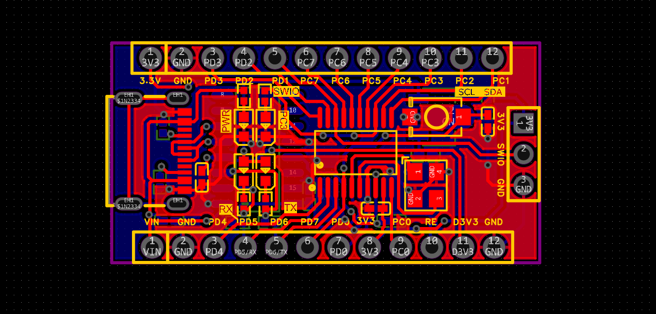
On a compact board like this one, crystal nets and programming pins should be treated as priority routes. The crystal traces to PA1 and PA2 need to be kept short with solid ground return paths, while the SWIO programming line needs clean access for both the programming header and test probes.
Preparing Schematics for Optimal DFM and Fabrication
Before you export Gerbers, go back to the schematic and verify these critical items:
- Confirm symbol-to-footprint mapping. Every schematic symbol must be mapped to the exact assembly footprint that matches the physical component you intend to use. A wrong pad pattern on even one component can scrap an entire production run.
- Ensure test and programming accessibility. On the WCH32V003 board, pads or headers for SWIO, NRST, and UART must be accessible for programming and debug. If these points are buried under components or placed on inner layers, firmware loading becomes impossible without rework.
- Pre-check panelization intent. If you plan to panelize your 34.976 mm x 17.998 mm board for volume production using tabs or mouse bites, plan the panel borders and tooling holes early. Schematic-level planning ensures that board edge connectors and mounting holes do not conflict with panel rails.
Modern manufacturers like JLCPCB offer online DFM checking tools that analyze your Gerber files for manufacturing issues. But those tools work best when the upstream schematic is already clean. A DFM tool can catch a drill hole that is too small, but it cannot fix a net that was never connected in the schematic.
How Professional Schematic Capture Drives Manufacturing Excellence
Reducing Revisions and Production Delays
Every ambiguity in your schematic generates an engineering question from the fabrication or assembly house. Each question adds hours or days to your production timeline. On a board with 29 components and 35 nets, even two or three unclear net assignments can trigger a review cycle that delays your order.
Early ERC combined with thorough library checks prevents PCB re-spins caused by simple symbol or pin mistakes. A misassigned pin on a USB-to-TTL bridge IC might pass a quick visual review but fail catastrophically in production. The few hours spent on rigorous schematic validation pay for themselves many times over in avoided re-spins.
Enabling Higher Yield and Lower Costs
Clear schematic intent directly improves DFM review quality and first-pass assembly yield. When the assembly house can read your schematic and immediately understand which component goes where, how power flows through the board, and what the programming interface looks like, they can optimize their pick-and-place setup and reflow profile with confidence.
Better part definition in the schematic reduces wrong-part placements and sourcing substitutions. When your BOM specifies exact manufacturer part numbers tied to verified schematic symbols, the risk of a purchasing agent substituting an incompatible component drops significantly. This is especially important for components like the CH32V003 MCU itself, where package variants exist with different pin counts and thermal pad configurations.
JLCPCB’s Expertise in Turning Great Schematics into Reliable Boards
The process of manufacture at JLCPCB is our additional lab mate that we all require: it provides a stress test of our design, and, in return, rewards us with feedback loops that make our schematic playbooks hold together. Their online DFM tools are displayed via the JLCDFM checker that crunches your files and identifies possible fab hiccups before a board hits the shop floor. In addition to that, their PCBA file instructions ensure that your BOM and CPL files are directly out of your schematic, else no confusion down the line.
Such a pro preview is a magnifying device rather than a guide to sweet schematic labour. Of course, a fab can pick up a misplaced footprint or a drill spec, but it is not going to pick up a raw circuit error. It is up to you, your design, and your project to create a clean schematic. When you give JLCPCB a clean, annotated schematic and they begin production at a cost of only 2$ per board, and you get the option of having the SMT assembly done, chances are that you will have a board that works as soon as you open it.
Frequently Asked Questions (FAQ)
Q1: What is the minimum schematic quality bar before starting layout?
At minimum, your schematic should pass a full ERC with zero unresolved errors, have consistent net naming across all sheets, and have every symbol linked to a verified footprint. All power rails must be explicitly labeled, all unused MCU pins must be marked as no-connect or properly terminated, and connector pin mappings must match the physical part datasheet.
Q2: How often should ERC be run in a small MCU board project?
Run ERC after completing each functional block: power regulation, clock circuitry, MCU connections, communication interfaces, and IO breakout. For a project like the WCH32V003 board with nine distinct functional blocks, that means at least four to five ERC runs during schematic development, plus a final comprehensive check before layout handoff.
Q3: How do I avoid symbol/footprint mismatches for production?
Always verify footprints against the component datasheet, not just the library default. Check pad dimensions, pin numbering, and thermal pad size. Use 3D model previews when available to visually confirm the footprint matches the physical component. Before generating manufacturing files, do a final cross-check of every component in your BOM against its assigned footprint.
Q4: Which nets should be treated as "must-verify" on CH32V003 boards before fabrication?
The critical nets to verify are: 3V3 and GND power distribution (continuity and decoupling), PD1/SWIO programming interface (connectivity to header and pull-up), PA1/OSCI and PA2/OSCO crystal connections (load capacitor values and ground returns), USB data lines D+ and D- (routing to the USB-to-TTL bridge).
Keep Learning
How Modular PCB Design Simplifies Complex Electronics Projects
Key Takeaway Modular PCB design simplifies complex electronics by breaking boards into independent, reusable functional blocks with clear interfaces. It boosts reusability, speeds up debugging, enhances team collaboration, and reduces errors.Shift from flat to modular design for faster development and more scalable, reliable PCBs. Ever seen a 400+ component schematic and got your head scrambled before even beginning routing? You are not alone. With the ever-increasing density of electronics combined w......
Your Ultimate Guide to PCB Rulers
In the world of PCB design and manufacturing, having the right tools is crucial for achieving accuracy and precision. One such tool that has gained popularity among professionals and hobbyists is the PCB ruler. This specialized measuring tool is designed to provide accurate measurements, reference information, and component footprints, assisting designers, engineers, technicians, and assemblers in various stages of PCB development. In this guide, we'll explore what a PCB ruler is, the features and mea......
Understanding the Materials Used in PCBs: Selection, Types, and Importance
Key Takeaways FR-4 is the go-to material for most cost-effective and reliable PCBs. Use Rogers for high-frequency and RF applications to reduce signal loss. Higher copper weight (2oz) improves current and heat handling. Choose High-Tg substrates for better thermal stability in multilayer boards. Green LPI soldermask offers the best balance of performance and inspection. Printed circuit boards (PCBs) are an essential component of modern electronics. These boards connect and support electronic component......
How to Select Tg of PCB ?
What is the Tg of PCB? In PCB manufacturing, "Tg" stands for Glass Transition Temperature. It is the temperature at which the PCB substrate material transitions from a rigid, glassy state to a soft, rubbery state. PCBs are flame-retardant (UL94 V-0) and do not burn easily; instead, they soften above Tg. The Critical Correlation Between Tg and Z-Axis CTE (Coefficient of Thermal Expansion) When the temperature exceeds the Tg point, the PCB substrate material (such as standard FR-4) undergoes a physical ......
How to Choose the Thickness of PCB
First, In the world of electronic products, the PCB is often referred to as the "heart" of the device. It interconnects all components, making board thickness one of the most important parameters. Choosing the right PCB thickness directly affects the electrical performance, mechanical stability, thermal management, and long-term reliability of the final electronic product. The process of selecting PCB thickness is influenced by various factors, such as product application scenarios, board material, an......
PCB Copper Pour Basics
What is Copper Pour in PCB Design? Copper pour refers to the technique of filling unused areas of a PCB's copper layers with solid copper planes. These planes are connected to power or ground nets, creating a continuous conductive path. Copper pour is typically used in the power and ground planes, as well as in signal layers for specific purposes. Purpose and Benefits of Copper Pour: Copper pour is primarily used to fill unused areas on PCB copper layers with solid (or hatched) copper connected to pow......