Advanced PCB Via Filling Options for Superior Signal Integrity and BGA Layouts
14 min
- Understanding PCB Via Filling and Its Role in High-Density Interconnects
- Exploring Different Types of Via Fill Techniques
- Implementing Via in Pad Technology for Compact Designs
- Advanced Manufacturing Excellence with JLCPCB Via Filling Solutions
- FAQ About PCB Via Fill
- Conclusion
Key Takeaways
- Prevents BGA solder wicking by sealing holes to stop solder from draining during reflow.
- Frees up routing space by using Type VII via-in-pad to eliminate dog-bone traces.
- Selects non-conductive resin for flat pads and copper-epoxy for heat transfer.
- Requires surface grinding to keep dimples under 25 microns for good paste printing.
- Uses cross-section coupons and flying probe tests to verify hidden fill quality.
A PCB via is normally a hollow plated hole, but that open structure creates a problem when you place it directly under a fine-pitch BGA pad. During reflow, solder can flow into the via and leave the BGA joint starved. Via filling solves this by sealing the hole and, in some cases, plating over it to create a flat surface. The result is better control of solder, more routing space, and a cleaner layout for high-density boards.
In this guide, you will learn:
- What does filling actually do inside a plated hole
- The seven IPC-4761 via protection types in plain words
- Non-conductive resin, copper-epoxy, and plated copper fill compared
- How via in pad frees routing space under a fine-pitch BGA
- Why does an unfilled via steal solder from a BGA ball
- Planarization, dimple limits, and the voids that cause rework
Understanding PCB Via Filling and Its Role in High-Density Interconnects
What is PCB Via Filling and How It Works
PCB via filling turns a hollow plated hole into a solid, sealed pillar. During fabrication, resin or metal is packed into the barrel, cured, ground flat, and covered with plated copper. This removes the open path that otherwise runs from one face of the board to the other.
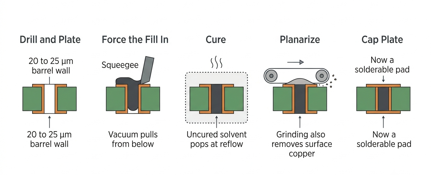
The sequence runs like this:
- Drill and plate the hole: Copper plating forms the barrel wall here, typically 20 µm (0.8 mil) average for IPC-6012 Class 2 and 25 µm (1.0 mil) for Class 3.
- Force the fill in: A squeegee or pressurized applicator pushes paste down the barrel while vacuum pulls from below.
- Cure the fill: Heat or UV hardens the paste. End curing early, and the solvent remains trapped in the hole.
- Planarize: A sander grinds the surface back until the fill sits level with the copper.
- Cap plate: A second plating cycle closes the top, turning the via into a solderable pad.
The fill must reach the whole barrel, because a partial fill leaves a pocket of air. It must also shrink as little as possible while curing, because shrinkage pulls the surface into a dip called a dimple. The governing document is IPC-4761, the design guide for via protection. It defines seven types, and only three involve filling the hole.
Key Electrical and Thermal Benefits of Via Fill in Modern Layouts
The practical truth is that filling a via barely changes its impedance. What it changes is where you are allowed to put the via, and that is what improves signal integrity. An unfilled via must sit beside the pad it serves, joined by a short escape trace that adds length to every net. Fill and cap it, and the via moves inside the pad, so that the trace disappears.
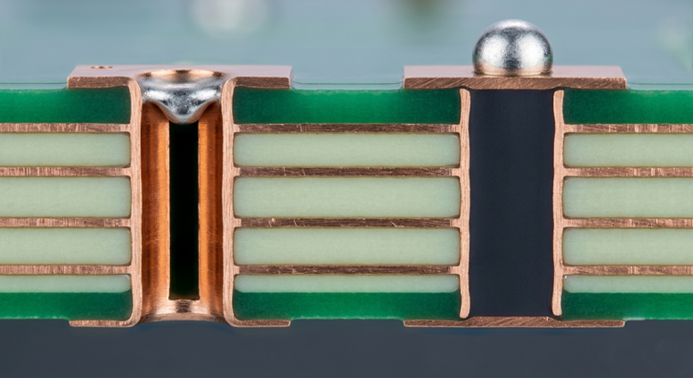
IPC-4761 lists the practical wins, and they are mostly about keeping things out of the hole:
- No loose solder balls: Trapped air in an open via can eject molten solder during reflow, leaving a loose conductive ball somewhere on your board.
- No mask creep and less paste loss: Liquid mask stops pooling in the barrel, and paste printed over a sealed pad stays on the pad.
- A reliable vacuum seal with no hidden flux: Pick-and-place nozzles and test fixtures depend on suction, which an open via leaks away. Once filled, the same via also gives flux nowhere to hide.
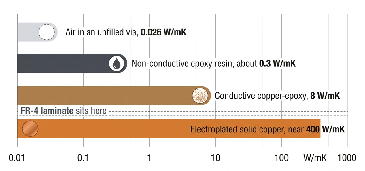
For heat flow, keep the fill's role clear. The copper barrel still carries most of the heat either way. Air in an open via moves about 0.026 W/mK, and non-conductive resin sits near 0.3 W/mK, roughly the same as the FR4 around it. Conductive copper-epoxy changes the result, reaching 8 W/mK in JLCPCB's published figure.
Exploring Different Types of Via Fill Techniques
Three words are often used interchangeably despite describing different structures: tented, plugged, and filled. Confusing these terms is the most common via specification error, and the fabricator builds exactly what your drawing note says.
Resin Non-Conductive vs. Copper-Filled Conductive Vias
There are three families of fill material, and they differ by roughly a factor of a thousand in how much heat they move.
| Fill Type | What It Is Made Of | Heat It Moves | Choose It When |
|---|---|---|---|
| Non-conductive epoxy resin | Polymer paste, thermally or UV cured, no metal | About 0.3 W/mK, similar to FR4 | You need a flat solderable pad, not a heat path. The default for via in pad |
| Conductive copper-epoxy | Polymer loaded with copper or silver particles | 8 W/mK on JLCPCB's published figure | The via array is doing thermal work under a power part |
| Electroplated solid copper | Bulk copper grown in the barrel, no polymer | Approaching 400 W/mK | Stacked microvias in HDI, or the highest thermal demand |
Thermal cycling creates a mechanical constraint that sales sheets rarely explain. Copper expands at about 17 ppm per degree C. Taiyo's THP-100DX1 gap-filling resin, a common non-conductive fill, expands at about 32 ppm below its glass transition temperature and about 115 ppm above it. As the board cycles, the resin pushes against a barrel that expands at a different rate. IPC-4761 states plainly that CTE mismatch is known to cause barrel cracks, and on a capped via, that stress shows up as a lifted pad.
Tented Vias, Plugged Vias, and Complete Epoxy Fill Options
Tenting is a film of a soldier's mask stretched over the hole like a drum skin, with nothing inside. Plugging pushes the material partway in. Filling packs the whole barrel. Only the third one seals the via.
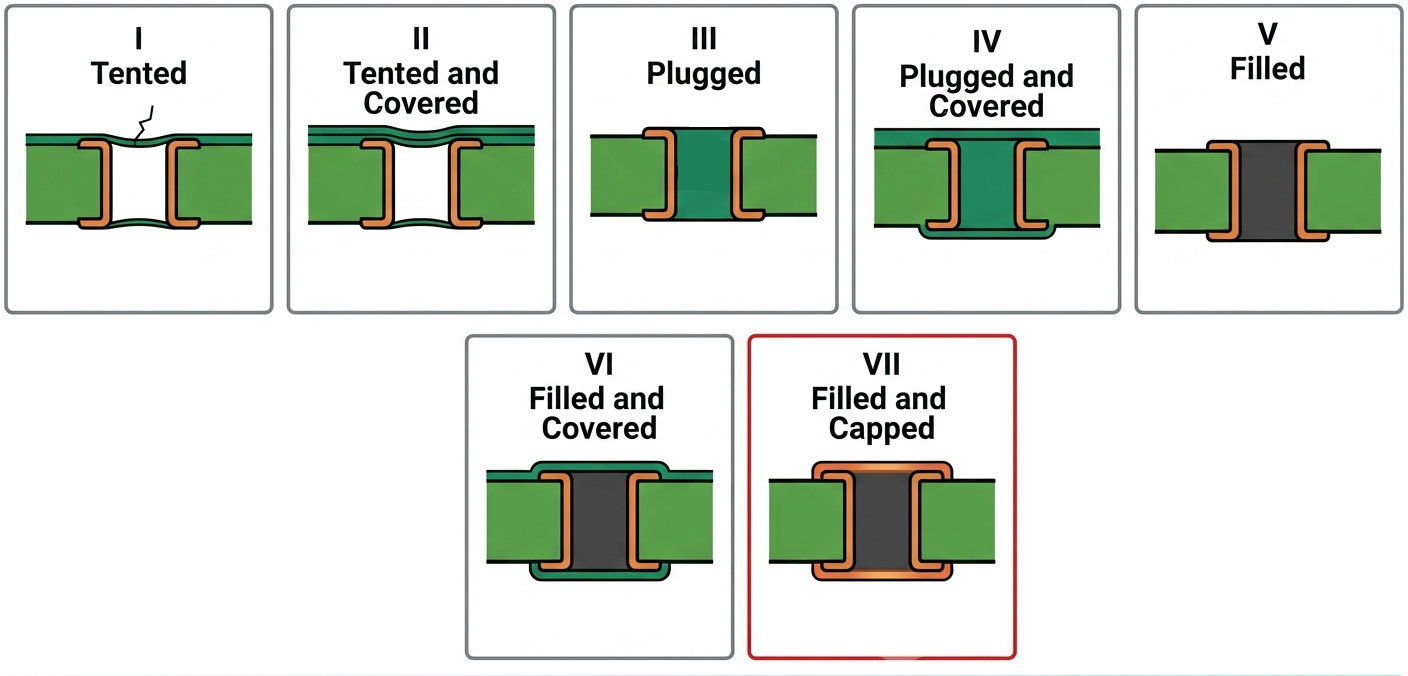
IPC-4761 sorts all of this into seven types:
| IPC-4761 Type | What Is In or Over the Hole | Hole Sealed? | Use It For |
|---|---|---|---|
| I: Tented | Dry film mask bridged over the opening | No, the film often opens | Signal vias away from pads, cheapest |
| II: Tented and Covered | Type I plus a second mask layer | No, but the tent is stronger | Tents that must survive handling |
| III: Plugged | Ink or resin pushed partway in | Partly, air is trapped in the middle | Blocking solder migration |
| IV: Plugged and Covered | Type III plus mask over the top | Partly, seals surface pinholes | Plugs that must stay opaque |
| V: Filled | Material driven through the full barrel | Yes | Vias inside cores, thermal fills |
| VI: Filled and Covered | Type V plus a mask layer over it | Yes | Filled vias needing a mask on the land |
| VII: Filled and Capped | Type V plus copper plated over both ends | Yes, and the top is solderable | Via in pad under a BGA |
Two details catch designers out. Tenting needs a dry film solder mask, because a liquid mask will not bridge a hole, and IPC-4761 calls for film at least 0.076 mm (3 mil) thick when the tent is not covered. A tented via is also a sealed air pocket, so reflow heat expands that air until the tent cracks or pops upward.
Implementing Via in Pad Technology for Compact Designs
Via in pad plated over, commonly called VIPPO, is a Type VII via built directly inside a component land. It is the only routing technique that scales below about 0.65 mm ball pitch, which is why a phone mainboard is a fraction of the size of a development board.
How Via in Pad Saves Board Real Estate in Fine-Pitch BGAs
The traditional escape is a dog bone: a short trace from the BGA pad out to a via placed in the gap between pads. It works until the gap runs out.
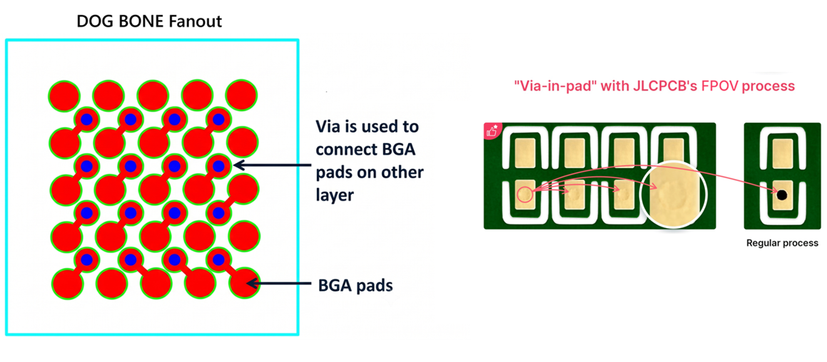
Example: An AMD Xilinx XC7A100T-FGG484 is 23 x 23 mm with 484 balls on a 1.0 mm pitch, leaving a comfortable channel for a via and a trace. An STM32H743XI in TFBGA240 drops to 0.8 mm pitch, and the channel gets tight. An nRF52840-CKAA in wafer-level chip scale runs 0.35 mm pitch with 0.212 mm pads, and there is no channel at all.
Take the 0.8 mm case. With a 0.4 mm pad, the gap between neighboring pads is 0.4 mm. JLCPCB's minimum finished via diameter is 0.25 mm, needing 0.2 mm clearance to copper on each side. The geometry demands 0.65 mm inside a 0.4 mm slot. At the third ring of balls, the dog bone escape no longer fits.
Via in pad changes the geometry completely:
- The escape trace disappears: Each dog bone carries 0.5 to 0.8 mm of trace, and a 484-ball part has 484 of them.
- The outer layer frees up: Space filled with fanout vias becomes a usable routing channel.
- Inner balls become reachable: A via straight down from the pad reaches any layer, so the ring count stops limiting you.
- Decoupling gets closer: A ground via inside the pad shortens the loop from ball to plane, cutting inductance.
Preventing Solder Wicking and Void Formation During Reflow
Put a via in a pad without filling it, and you have built a drain. IPC-4761 puts it bluntly: vias can act as a thermal path that draws solder volume away from the joint.
The volume comparison shows why this matters. A 0.3 mm via through a 1.6 mm board holds about 0.11 mm³ of empty space. A 0.8 mm-pitch BGA ball is only around 0.45 mm wide, with roughly 0.05 mm³ of solder. So an unfilled via can readily absorb more solder than the entire BGA ball contains. The result is a solder-starved joint that may still pass a basic bench test, making it easy to miss. The real failure can show up later under vibration or thermal cycling.
The second issue is outgassing, usually caused by incomplete curing. UV light cannot fully reach the bottom of a deep via, leaving solvent trapped inside. During reflow, that solvent heats up, expands, and can create voids or other defects.
Advanced Manufacturing Excellence with JLCPCB Via Filling Solutions
Executing the process matters as much as writing the via fill specification. Fill percentage, cure completeness, and surface flatness are factory-floor variables, so confirm exactly what your fabricator actually commits to.
High-Precision Automated Resin Plugging and Planarization Capabilities
Planarization is the least discussed and most consequential step. The fabricator deliberately overfills the via to guarantee a complete barrel, leaving a raised bump of cured resin standing above the copper surface. A sander grinds it back until the surface is level, and only then does cap plating go on. That grinding removes surface copper, too, which is why IPC-4761's sample drawing note limits the loss to 50% of the specified minimum plated surface copper.
The tolerance that matters afterward is the dimple, the small dip left where the fill shrank during cure. IPC-4761 does not name a number; it tells the designer and fabricator to agree on one. Most fab drawings for BGA pads call for a dimple or protrusion no greater than 25 µm (1 mil), tightening toward 15 µm for Class 3 work. IPC-4761 records that a bump height of 0.076 mm (3 mil) or more lifts the stencil off the board, breaking the gasket seal around every nearby aperture. One badly planarized via ruins the print for its neighbors.
JLCPCB publishes the following via specifications:
- Minimum via hole 0.15 mm (6 mil), minimum finished diameter 0.25 mm (10 mil), the diameter is at least 0.1 mm larger than the hole.
- Tented vias ideally 0.4 mm (16 mil) or less, 0.5 mm (20 mil) maximum, because mask film cannot bridge a wider opening.
- Plugged vias with ink, better than 98% plugging rate and better than 95% opacity.
- Epoxy-filled and capped, resin planarized and plated over with copper, for vias up to 0.5 mm (20 mil).
- Copper-epoxy filled and capped at 8 W/mK, for arrays carrying heat as well as current.
Integrated Quality Inspection with X-Ray and Flying Probe Testing
A filled via hides its own defects: a void inside the fill, incomplete cap plating, and a crack in the barrel wall. Each type of failure needs a different inspection instrument.
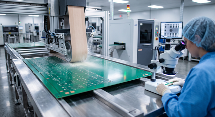
- Cross-section coupons catch voids: Resin has no metal in it, so it is nearly invisible to X-rays. The only way to see a bubble in the fill, or fill that has separated from the knee of the barrel, is to cut a sacrificial coupon from the panel edge and study the polished face under a microscope. IPC-4761 treats that separation as a void because it traps chemistry against the copper.
- X-ray catches the consequences: X-ray sees metal, so it is the tool for what sits above the via rather than inside it. On an assembled board, it shows voiding inside the BGA ball, the exact defect that a dimple or an outgassing plug produces.
- Electrical test catches opens: A flying probe checks each net against the netlist, so a cap that failed to plate through or a barrel cracked by CTE stress appears as an open. Filled vias help again here, because IPC-4761 notes that unfilled holes leak air and cause intermittent probe contact in vacuum-based test fixtures.
FAQ About PCB Via Fill
Q: What is the difference between a tented via and a filled via?
A tented via has a film of dry solder mask stretched over the opening with nothing inside. A filled via has the whole barrel packed with cured resin or metal. Only a filled and capped via gives you a solderable surface.
Q: How much solder can an unfilled via steal from a BGA ball?
More than the whole ball. A 0.3 mm (12 mil) via through a 1.6 mm (63 mil) board holds about 0.11 mm³ of space, while a 0.45 mm BGA ball is roughly 0.05 mm³ of solder. The barrel holds more than twice that volume.
Q: Should I use conductive or non-conductive via fill?
Use non-conductive epoxy resin for via in pad, where the goal is a flat, solderable surface. Use conductive copper-epoxy, around 8 W/mK, only when the array carries real heat from a power component. It costs several times more and buys nothing on a signal via.
Q: What is a dimple, and how flat does the finished pad need to be?
A dimple is the small dip left in the pad after the fill shrinks during cure. IPC-4761 leaves the limit to the designer and fabricator, but most BGA drawings call for no more than 25 µm (1 mil). Bumps of 0.076 mm (3 mil) or more lift the stencil and ruin the paste print nearby.
Q: Does via filling cost extra?
Costs depend on layer count and fabricator. JLCPCB includes resin filling/POFV as standard at no charge on 6-layer through 20-layer boards, while POFV on a 4-layer board is charged. Copper-epoxy fill is a separate, more expensive process.
Conclusion
The most useful shift in thinking about PCB via fill is to stop treating it as a surface finish option and start treating it as a structural decision. Tenting manages what crosses the board. Filling and capping change what the via is, converting a hollow tube into a solid, solderable pillar you can place anywhere, including inside a component land. That distinction also determines the material: resin buys a flat pad, copper-epoxy buys a heat path, and neither substitutes for the other.
Component pitches keep shrinking, and every step down pushes more designs from optional via in pad toward mandatory. With resin filling and POFV standard on 6-layer and higher boards at JLCPCB, the old cost barrier has largely disappeared. What remains is specifying the process correctly, which takes only one drawing note.

Keep Learning
Understanding SMT PCB Boards Technology: An Essential Component of Modern Electronics
Surface Mount Technology (SMT) has changed manufacturing of modern electronics. It has made designs and assembly methods more efficient. Many modern electronics depend on SMT PCB boards, which make it possible for circuit designs to be small and efficient. This is what today's technology needs. This article discuss about many types of SMT PCB boards, their uses, and the best methods for designing and assembling them. 1. What is an SMT PCB Board? Printed circuit boards called SMT PCB boards, use surfac......
How to Choose the Right Prepreg Material for Reliable Multilayer PCB
Have you ever wondered what makes all those copper layers stick to a cross-section of a multilayer PCB? Prepreg material is the answer, and it is of much more importance than most engineers think it is. Choose the prepreg selection wrong, and you are predetermined to delamination, impedance drift, and long-term reliability problems. Prepreg is not only glue. It is a designed composite that determines your dielectric separation, dictates your impedance, affects signal loss, and determines your board be......
Via Filling Explained: Key Techniques, Benefits, and Solutions for High-Performance PCBs
Key Takeaways Via filling completely fills plated through-holes and microvias with epoxy or conductive copper paste, followed by planarization and copper capping (POFV). It eliminates voids, solder wicking, and thermal/mechanical issues while enabling reliable via-in-pad designs. Benefits include superior heat dissipation (up to 8 W/m·K), better signal integrity, higher mechanical strength, and improved assembly yields. JLCPCB provides free non-conductive filling + POFV on 6+ layer boards. Ideal for H......
How Fiducial Markers Guarantee Perfect Alignment in Professional PCB Fabrication
Today, the most sophisticated pick-and-place machine can place a 0.5 mm pitch QFP on its footprint, board after board, thousands of times, and never miss. It is not only a matter of expensive cameras or high-quality servos, but it begins with a little, very small copper dot, simply hanging there in the corner of your PCB. That dot represents a fiducial marker, and without it, even the smoothest SMT line would be laying components in the dark. The unrecognized heroes of automated assembly are the fiduc......
Technical Guidance: Character Design Specifications
To facilitate component assembly, future maintenance, and traceability of PCB manufacturing information (such as manufacturer, production date, batch number, etc.), various character markings are typically silk-screened onto the PCB. These include component designators, polarity marks, test point labels, company logos, and production traceability information. Traditional PCB character silk-screening uses the screen printing process, hence the term “silk-screen characters.” High-definition characters a......
Step-by-Step Guide to the Printed Circuit Board Manufacturing Process
Key Takeaways Core Role: PCBs provide the physical foundation and electrical connections for modern electronics. Multi-Step Process: Manufacturing spans design imaging, substrate creation, inner/outer layer etching, lamination, and surface finishing. Precision & Quality Control: Features micro-drilling (down to 100 µm) for layer connectivity, Automated Optical Inspection (AOI), and final electrical testing. Protection & Finish: Solder masks and surface finishes (e.g., ENIG, HASL) protect copper traces......