
How PCB Cross Section Analysis Ensures Flawless Multilayer PCB Quality
12 min
- Key Insights Revealed by PCB Cross Section
- Best Practices for Effective Cross-Section Analysis
- Manufacturing Benefits of Routine Cross-Section Analysis
- JLCPCB's Advanced Cross-Section Capabilities
- Frequently Asked Questions (FAQ)
Ever wondered what is really under a multilayer PCB? A completed board appears to us as a student as a flat and homogeneous slab of laminate and copper, yet internally a maze of plated vias, buried copper layers, thin dielectric films, and resin-filled structures, all of which must be within very strict tolerances. Cross-section analysis is the PCB equivalent of peeling back the layers and getting the true picture. Every person involved in PCB design or manufacturing, in a laboratory or on a production line, is aware that learning how to cross-section-analyze is not a choice; it is the surest method of ensuring that what we put down on screen reflects on the actual board in the fab.
It is used whether you are creating a 4-layered prototype of a consumer device or a 30-layered backplane of an aerospace project; this technique exposes defects that cannot be detected by other inspection techniques. Today, we will discuss how PCB cross-section analysis, start to finish, what it can tell us about the internal quality of the board, the best practices that can distinguish solid analysis and great analysis, and how big organizations such as JLCPCB have incorporated it into their quality systems. Let’s dive in.
What PCB Cross-Section Analysis Is and How It Works
Microsectioning Analysis PCB cross-section analysis, or microsectioning or metallographic analysis, is simply a destructive method of inspecting the interior of a printed circuit board. The most important word here is destructive. You are actually cutting in the board, unlike X-ray or AOI, and the sample is not a finished product. The trade-off is justified, since there is no other approach that will provide you with that kind of detail. It is a rather strict process. The engineer then selects a point on which to examine, typically a through-hole (PTH), a microvia, or a layer transition point where the defects tend to be most noticeable.
The piece is then sliced out of the panel by a precision low-speed diamond saw. The piece cut is placed in a clear epoxy resin in a mounting cup (typically 25 to 32mm in diameter) and left to dry. When it is installed, the actual preparation begins. The sample is lapped with successively finer silicon carbide (SiC) abrasive papers - beginning with 120 -grit and continuing through 240, 320, 600, 800, and finally, 1200 -grit. Finally, the polishing is done after grinding using alumina or diamond suspensions to a particle size of 0.05 microns. To ensure that you have a smooth surface with no scratches, the rotation of the sample is reversed between grit stages.
Why It Is Essential for Multilayer and HDI Boards
Four-plus-layer multilayer PCBs possess very complicated inner designs immeasurable with surface inspection tools or Automated Optical Inspection (AOI). You simply would not be able to see a buried via, a delaminated prepreg layer, or a resin void on the surface. It is where cross-sectional analysis comes in with no substitute. The difficulty is further increased by the High-Density Interconnect (HDI) boards. Microvias in HDI designs are typically 75-150 microns in diameter, stacked and staggered, and dielectric layers are typically less than 75 microns in thickness.
At these small scales, a minor variation of the process can cause open circuits, unreliable connections, or concealed failures that only manifest themselves in the field. Non-destructive tests, such as X-ray, are excellent in inspecting component positioning, solder joint configuration, and general orientation. However, they have no idea of the actual copper thickness, the structure of copper grains, or micrometric inter-layer delamination. Cross-section analysis is actually the only game in town in terms of those critical details.
Key Insights Revealed by PCB Cross Section
Layer Thickness, Copper Plating, and Delamination Detection
One of the most fundamental measurements from a PCB cross-section is the thickness of each individual layer. This includes copper foil layers, prepreg bonding layers, and core laminate layers. Every one of these must fall within the design specification and the applicable IPC tolerances. A cross-section provides direct, accurate measurement of all of them in a single view.
| Copper Weight (oz) | Nominal Thickness (microns) | Nominal Thickness (mils) |
| 0.5 oz | 17.5 | 0.7 |
| 1 oz | 35 | 1.4 |
| 2 oz | 70 | 2.8 |
| 3 oz | 105 | 4.2 |
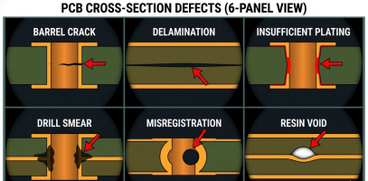
In addition to copper, delamination, or the separation between laminate layers due to moisture, thermal stress, or poor bonding during lamination, is visible in the cross-section. It also reveals drill smear, in which the resin used in the drilling lines coats the inner copper layers and prevents them from connecting to electricity. Another common occurrence is resin voids, tiny pockets in which the resin did not laminate.
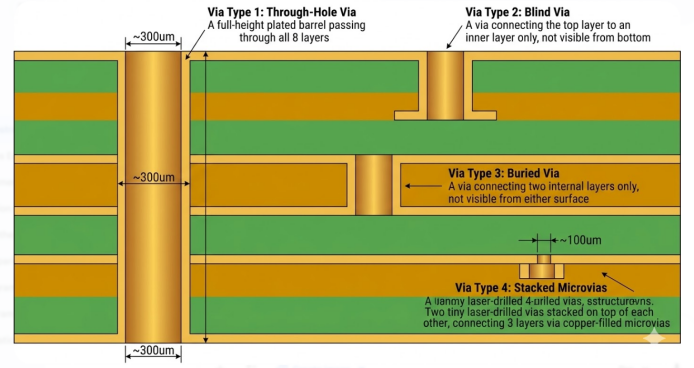
Via Quality, Alignment, and Interlayer Integrity
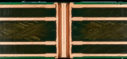
One of the most examined aspects of a cross-section is via integrity. The via barrel is the cylindrical copper plating within a hole that has been drilled; it must have no cracks. A popular thermal cycling failure mode is barrel cracks. The expansion of the laminate on the Z axis during heating and cooling of the board is what puts stress on the copper barrel. These cracks can only be detected by cross-sectioning before they lead to field failures.
Microvias of HDI are also treated with special concern in the cross-section analysis. The engineer checks the shape of the microvia (it should be a clean and slightly conical profile), the depth, the amount of copper that has been covered on the walls of the via, the dimple depth at the top, and the percentage of voids. The aspect ratio of microvia (depth/diameter) is generally restricted to 1:1 in order to be able to plate and fill it reliably. Another important measurement is layer-to-layer registration. The copper pad that is left around a hole to be drilled must be of IPC minimums. In Class 3 external layers, the lowest annular ring is 50 microns.
Best Practices for Effective Cross-Section Analysis
Sample Preparation and Sectioning Techniques
Frankly speaking, the quality of a cross-section is all up to the way the sample is prepared. When you go wrong, you will have scratches, smears, or edge rounding that conceals true details and could even create artificial ones. The first thing you need to do is to choose the right spot. The majority of production panels are provided with test coupons, just small patches that replicate the via structure and the layer stackup of the actual board.
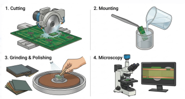
After cutting it, pour the sample into transparent epoxy with a mounting cup, typically with an area of 25 to 32mm in diameter. The use of clear resin is important since it allows you to observe the grinding in real time and when you are close to the desired plane. Once the epoxy has hardened, you polish the surface using a progression of SiC papers, 120, 240, 320, 600, 800, 1200 grit. The final, ly polish with diamond or alumina suspensions, to a minimum diameter of approximately 0.05 u m. It is hoped to achieve a mirror-like finish in which all the copper, resin, and glass fibers are on a single plane with no bumps or rounding out.
The complete sample preparation sequence is:
- Select the region of interest (via PTH or layer transition) from a test coupon.
- Cut the sample using a low-speed diamond saw to avoid thermal or mechanical damage.
- Mount the sample in clear epoxy resin in a 25-32 mm mounting cup and allow full cure.
- Grind through SiC papers: 120, 240, 320, 600, 800, and 1200 grit, rotating 90 degrees between stages.
- Polish with diamond or alumina suspensions down to 0.05 microns.
- Clean the sample ultrasonically between polishing stages to prevent cross-contamination.
- Optionally etch with ammonium persulfate to reveal copper grain structure.
Microscopic Examination and Measurement Standards
After having prepared the sample, we primarily look at the sample using optical microscopy. The typical magnifications are approximately 50X to approximately 500X, which is sufficient to measure the copper thickness, dielectric separation, the annular rings, and identify any delamination or voids. We attach a digital camera to the lens, take high-resolution images, and then feed them into a calibrated measurement program that ejects dimensions with a 1-2 micron error margin.
The reference to be used when verifying the results of those cross-sections is IPC-A-600, Acceptability of Printed Boards. It contains numerous photographic samples of good and bad conditions on Class 1, 2, and 3 boards. The measurement criteria are based on IPC-6012, which gives the dimensional specifications of rigid PCBs. These two standards combined provide the protocol for pass or fail.
Manufacturing Benefits of Routine Cross-Section Analysis
Early Detection of Process Issues and Improved Yield
I have also understood that regular cross-section analysis is essentially a very simple kind of early warning system that detects process drift. Think of plating baths that wear out, drill bits that wear out, lamination press temperatures that change, chemical concentrations that vary, all these slow changes remain unnoticed in the normal day-to-day operations until they one day lead to a batch of plating failing.
This is particularly handy when introducing a new product (NPI) and first-article inspection. An initial cross-section of the first article will ensure that the process parameters are really giving us boards that satisfy all the specifications, before we commit to a complete production run. Identifying a problem at the coupon level is a fraction of the cost of having to rework an entire lot, and it is much more desirable than having to address a field failure in the future.
The key manufacturing benefits include:
- Early detection of plating thickness drift before it causes rejections
- Verification of lamination quality, including bond strength and void content
- Validation of new materials, processes, or equipment before full production
- Reduced scrap rates through proactive process correction
- Compliance evidence for customer audits and certification bodies
Ensuring Consistent Quality Across Production Runs
Only some of the major PCB manufacturers apply SPC to cross-section measurements. In essence, they maintain records of copper plating thickness, dielectric thickness, dimensions of the annular rings, and other materials in order to develop control charts that show process trends and their capacity. Process capability has an industry target of a Cpk of more than 1.33, which implies that the process is centred within its specification limits with a healthy margin.
In high-reliability applications, cross-section analysis is not only a best practice but a necessity. The aerospace standards AS9100 and automotive quality systems under IATF16949 also require objective evidence of internal board quality, and cross-sections are just that.
JLCPCB's Advanced Cross-Section Capabilities
State-of-the-Art Equipment and Expert Analysis Team
JLCPCB maintains its cross-section suite, such as precision diamond saws, auto-grinders and polishers, high-res metallographic microscopes with calibrated digital imaging. That equipment allows the quality department to perform entire tests within the premises, thus there is no need to outsource to laboratories- quicker response and more in touch with the manufacturing process.
The team of analysts consists of trained metallographers who completely understand IPC standards, such as IPC-A-600 acceptability and IPC-TM-650 test methods. They are able to provide same-day or next-day turnaround on urgent checks, and therefore, the production lines are not stalled waiting to get the results. The speed is extremely convenient when performing first-article tests or in the process of tracking down a suspect process hiccup.
Integrated Quality Control from Prototype to Volume
JLCPCB is not a situation where cross-sectioning is a single instance. It is integrated into a larger QC system, which includes AOI, electrical testing (flying probe and fixture-based), and impedance testing. They also take cross-sections at multiple phases: initially, when qualifying a process, then when inspecting first-article parts of a new design, and also during process monitoring.
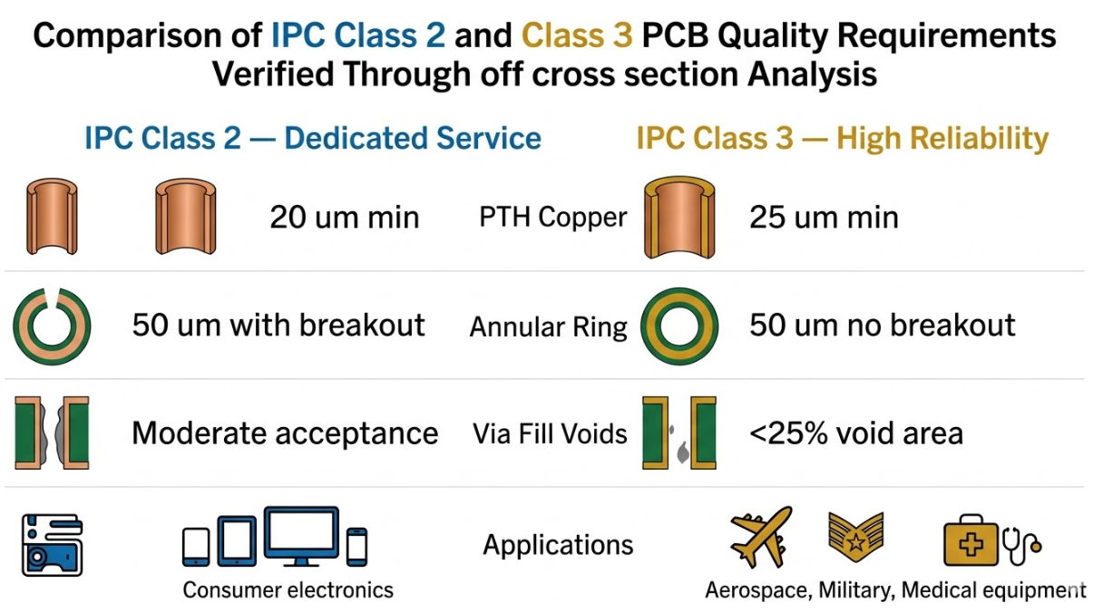
JLCPCB manufactures 1-14+ layers of boards, and the plant has an ISO 9001, UL listing, and is able to produce boards that can reach IPC Class 2 and Class 3. It does not matter whether you are getting a fast prototype at a cost of only $2 or you are going to large-scale production, the quality framework remains the same. The combination of cross-sectional analysis and the general QC toolkit implies that information on all inspection methods is input to a single, plugged-in board quality view.
Frequently Asked Questions (FAQ)
Q1: What is PCB cross-section analysis, and why is it important?
PCB cross-section analysis is a destructive inspection technique where a board sample is cut, mounted in epoxy, ground, polished, and examined under a microscope to reveal its internal structure.
Q2: What defects can cross-section analysis detect in a multilayer PCB?
Cross-section analysis can detect a wide range of defects, including insufficient copper plating in vias and PTHs, delamination between layers, resin voids, drill smear, barrel cracks from thermal cycling, poor via fill quality, and microvia defects.
Q3: What IPC standards govern PCB cross-section analysis?
The primary standards are IPC-TM-650 Test Method 2.1.1 (which defines the microsectioning procedure), IPC-A-600 (Acceptability of Printed Boards, which provides photographic accept/reject criteria), and IPC-6012 (Qualification and Performance Specification for Rigid PCBs, which defines the dimensional requirements that cross-section measurements are compared against).
Q4: How is a PCB cross-section sample prepared?
The sample, typically a test coupon from the production panel, is cut with a low-speed diamond saw, mounted in clear epoxy resin, and ground through progressively finer SiC abrasive papers from 120 to 1200 grit.
Q5: How often should cross-sectional analysis be performed during PCB production?
Cross-section analysis should be performed at several key stages: during initial process qualification for a new product or material, at first-article inspection for every new design, and at regular intervals during production runs (the frequency depends on volume and reliability class).
![]()
Keep Learning
Solder Joint Inspection in PCB Manufacturing : A Complete Guide to Catching Defects Early
Key Takeaways Solder Joint Inspection is critical in modern PCB manufacturing to catch defects early and ensure product reliability. By combining Solder Paste Inspection (SPI), 3D AOI for visible joints, and X-ray for hidden BGA/QFN issues, manufacturers can effectively detect common defects such as bridging, cold joints, tombstoning, and head-in-pillow. Following IPC-A-610 standards with a layered inspection strategy significantly reduces field failures while improving first-pass yield. JLCPCB’s prof......
3D AOI Inspection Explained : How It Catches Defects That 2D Systems Miss
Key Takeaways 3D AOI Inspection has become essential in modern PCB assembly by using advanced height and volume measurement to detect critical solder defects that traditional 2D AOI systems routinely miss, such as lifted leads, insufficient solder, head-in-pillow, and component coplanarity issues. By delivering precise 3D data through structured light or Moire technology, it significantly reduces false calls, improves first-pass yield, and ensures long-term reliability according to IPC-A-610 standards......
How Sustainable Materials and Expert Manufacturing Ensure RoHS Compliant PCBs
Have you ever experienced that a finished shipment of products was detained at the EU customs due to a single component on the board not passing the RoHS screening? It is higher than most engineers think, and the financial blow is far bigger than the impounded goods. Wasted time, remodeling expenses, and a compliance audit that is capable of halting your whole product introduction, that is the actual cost of doing RoHS wrong. The point is as follows: RoHS-compliant PCBs cease to be a checkbox exercise......
Preventing PCB Warping: Best Practices for Design and Manufacturing
In the design and manufacturing process of electronic equipment, PCB (Printed Circuit Board) warpage is a common but troublesome problem. PCB warping not only affects the performance and reliability of the device but can also cause connectivity issues and other serious consequences. Therefore, it is crucial to understand how to prevent and resolve PCB warping. This article will explore some best practices in design and manufacturing to help you effectively prevent PCB warpage problems from occurring. ......
PCB Cleanliness in Professional Manufacturing : Preventing Contamination and Ensuring Long-Term Reliability
In the construction of PCBs, the boards are contaminated with all sorts of dirt at almost every stage. In the soldering process, the flux (either rosin-based or more recent organic forms) may cause residues or ionic salts to remain on the pads and traces and be sticky. Next there is etching, plating and micro-etching; the chemical processes will put metal ions on the copper unless the rinsing is complete. Tiny particles of metal shavings, fiberglass dust, and laminate fragments are also thrown out in ......
PCB Basics 5: PCB Testing and Quality Assurance
Welcome to the realm of PCB testing and quality assurance! Quality control is always a crucial part of different industries. Great quality control not only could generate more energy for customers’ electronic projects, but it could also embark on certification and guarantee to the electronic industry. Let’s learn the importance of testing and quality assurance in PCB manufacturing. The Significance of Testing and Quality Assurance in PCB Manufacturing: Testing and quality assurance are extremely impor......