
Zener Diode vs Schottky Diode: Which One Should You Use?
16 min
- Zener Diode vs Schottky Diode: Quick Comparison
- Key Differences Between Zener Diodes and Schottky Diodes
- What Is a Zener Diode?
- What Is a Schottky Diode?
- Zener vs. Schottky Diode Symbol: How to Tell Them Apart
- Zener Diode vs. Schottky Diode: Electrical Characteristics
- When to Use a Zener Diode vs Schottky Diode
- Can a Schottky Diode Replace a Zener Diode (or Vice Versa)?
- Common Pitfalls When Using Schottky Diodes and Zener Diodes
- Zener Diode vs Schottky Diode: Package Selection and PCB Layout
- FAQs about Zener Diode vs Schottky Diode
- Conclusion
Zener and Schottky diodes may look identical in their physical surface-mount packages, but they serve completely different purposes in electronic design. A Zener diode is engineered specifically to operate in its reverse breakdown region for voltage regulation and overvoltage protection. Conversely, a Schottky diode is optimized for low forward voltage drop and high-speed switching in the forward conduction region.
This guide provides a comprehensive comparison of their operating principles, electrical characteristics, applications, packaging options, and real-world design considerations so you can confidently select the right diode for your next PCB assembly project.
Zener Diode vs Schottky Diode: Quick Comparison
Before diving into the detailed physics and design equations, let us review the high-level differences between these two common components.
| Parameter | Zener Diode | Schottky Diode |
|---|---|---|
| Junction type | Heavily doped P-N silicon junction | Metal to N-type semiconductor barrier |
| Carrier conduction | Bipolar (both electrons and holes) | Majority carrier only (unipolar conduction) |
| Forward voltage (Vf) | Typical silicon drop: 0.6 V to 0.7 V | Ultra-low: 0.2 V to 0.5 V |
| Designed operating region | Reverse breakdown region | Forward conduction region |
| Reverse characteristic | Precise, stable Zener voltage (Vz: 2.4 V to >200 V) | Rated peak reverse voltage (VRRM); exceeding it is destructive |
| Reverse leakage at 25°C | Extremely low (typically nA to low micro-amps) | Significantly higher (micro-amps to mA); rises exponentially with temperature |
| Reverse recovery time (trr) | Finite (tens of nanoseconds to microseconds) | Near-zero (no minority carrier charge storage) |
| Thermal runaway risk | Very low under recommended operating limits | Highly significant at ambient temperatures above 85°C |
| Primary circuit role | Voltage regulation, signal clamping, voltage reference | Power rectification, freewheeling, reverse polarity protection |
| Common SMD packages | SOD-123, SOT-23, SOD-323 | SMA, SMB, SMC (DO-214 family), SOD-123 |
Key Differences Between Zener Diodes and Schottky Diodes
Operating Principle
A Zener diode relies on reverse-bias breakdown. When the reverse voltage applied to its terminals reaches a specific threshold (Vz), the diode allows current to flow backward while clamping and holding the voltage drop remarkably stable.
A Schottky diode operates in the forward-bias direction. By substituting a metal-semiconductor interface for the traditional P-N semiconductor junction, it conducts forward current with a much smaller internal barrier and avoids the charge storage delays common to silicon diodes.
Forward Voltage Drop
Zener diodes display a standard silicon forward voltage drop of approximately 0.6 V to 0.7 V. Schottky diodes offer a highly efficient forward voltage drop of only 0.2 V to 0.5 V, depending on current density. This exceptionally low forward voltage drop directly translates to minimized power dissipation and higher conversion efficiency in power delivery paths.
Reverse Characteristics
While a Zener diode is specifically designed to operate indefinitely at its designated Zener breakdown voltage (Vz), a Schottky diode must be kept well below its maximum rated peak reverse voltage (VRRM). There is no controlled or safe breakdown mechanism in a Schottky diode; subjecting it to overvoltage beyond its VRRM rating will quickly degrade or destroy the barrier.
Switching Speed
Because they utilize the majority charge carriers (electrons) for conduction, Schottky diodes switch states almost instantaneously. There are no stored minority carriers to sweep away, resulting in an effectively zero reverse recovery time (trr).
Zener diodes contain heavily doped P-N junctions with high minority carrier densities, giving them a finite, measurable trr. Utilizing a Zener as a high-frequency switching rectifier can result in massive, destructive current spikes at switching nodes. This occurs because the slow turn-off transition causes a momentary short-circuit (shoot-through) when the complementary active switch turns on, generating excessive Electromagnetic Interference (EMI) and power losses.
Typical Applications
Zeners are ideal for static or low-speed voltage-control circuits: shunt regulators, voltage references, MOSFET gate clamps, and analog-to-digital converter (ADC) input protection.
Schottky diodes are the standard choice for moving raw current efficiently: switch-mode power supply (SMPS) rectifiers, freewheeling paths, reverse polarity protection, battery/USB power OR-ing, and high-frequency RF detector stages. If you are preparing to layout your power stage, you can evaluate the physical dimensions of both types of diodes in the solder pad design guide to ensure optimal heat dissipation and manufacturing yield.
What Is a Zener Diode?
A Zener diode is a specialized silicon P-N junction diode that has been heavily doped during manufacturing to narrow the depletion region. While it behaves like a standard diode in forward bias, its primary value lies in its predictable behavior under reverse-bias conditions.
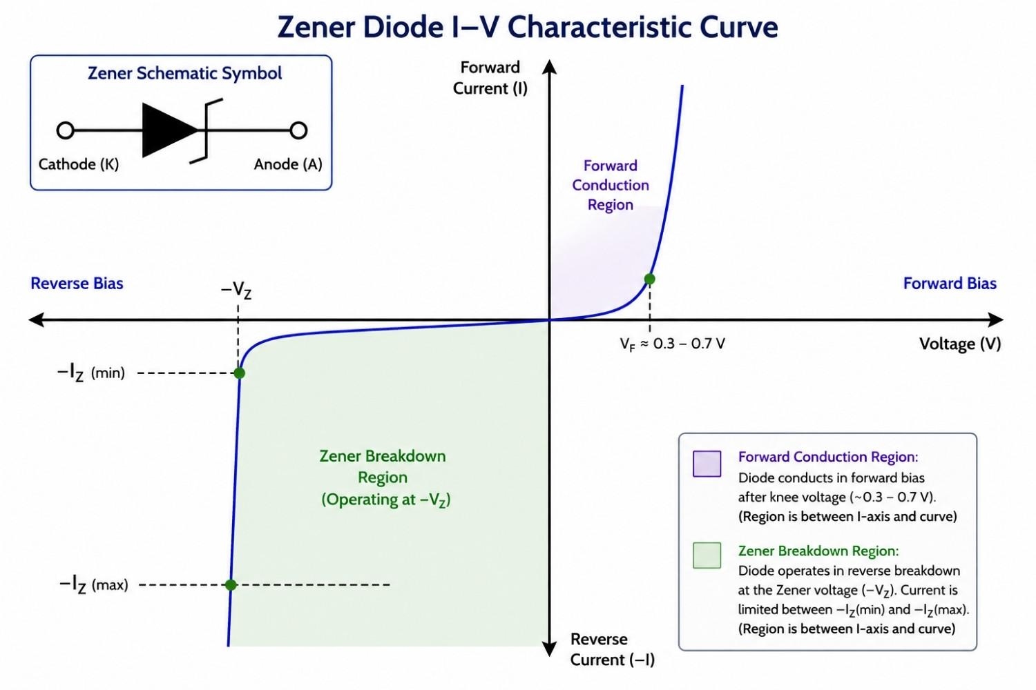
Figure: Zener diode I-V characteristic curve with schematic symbol inset.
Zener vs. Avalanche Breakdown
Engineers often refer to all reverse-breakdown diodes as "Zeners," but the physics behind their operation changes depending on the voltage threshold:
- The Zener Effect (Below 5 V): Under strong electric fields across a very narrow depletion region, electrons are pulled directly from the valence band to the conduction band via quantum tunneling. This effect has a negative temperature coefficient (TC) - the breakdown voltage decreases as the junction temperature rises.
- The Avalanche Effect (Above 5.6 V): High-energy carriers accelerated by the electric field collide with the crystal lattice, knocking free more electrons in a cascading impact ionization process. This mechanism exhibits a positive temperature coefficient—the breakdown voltage increases as temperature rises.
- The Sweet Spot (Around 5.6 V): At approximately 5.6 V, the negative temperature coefficient of the Zener effect and the positive temperature coefficient of the Avalanche effect cancel each other out. This produces a highly stable reference with near-zero voltage drift over temperature, making parts like the BZX84-C5V6 an industry favorite for precision sensing applications.
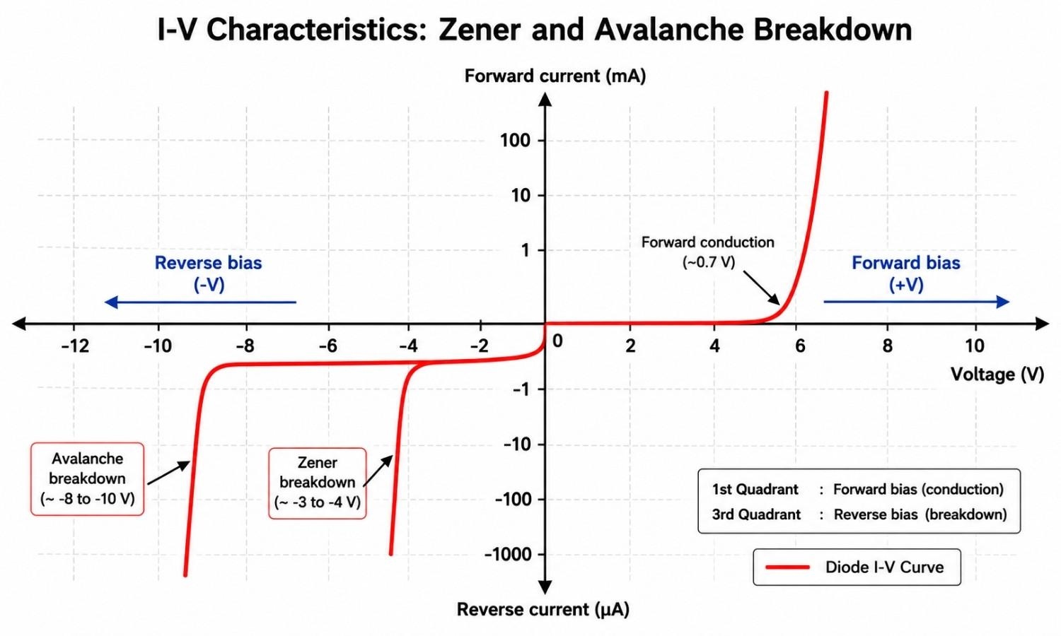
Figure: Single-panel I-V curve comparing Zener breakdown and Avalanche breakdown regions side by side under reverse bias.
Key Zener Diode Parameters
When sourcing components from the JLCPCB Parts Library, pay close attention to these parameters:
- Vz (Zener Voltage): This is the clamped voltage measured at a specific test current (IZT). For instance, a standard 1N4733A specifies a Vz of 5.1 V at an IZT of 49 mA, with a maximum dynamic impedance (Zzt) of 7 Ohms. Dynamic impedance represents the internal resistance of the Zener in its breakdown state. A lower dynamic impedance is critical for voltage regulation because it ensures the regulated Vz remains stable even if the current flowing through the diode fluctuates.
- Power Dissipation (Pd): The maximum thermal energy the package can safely dissipate. For a shunt regulator circuit, you must calculate the worst-case power dissipation when the load is completely disconnected:
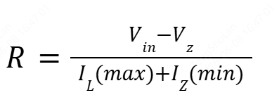
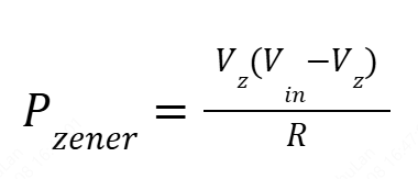
Failing to calculate this power dissipation correctly at cold start or open-load conditions is the most common reason shunt regulators fail in production.
What Is a Schottky Diode?
Unlike standard semiconductor diodes, a Schottky diode features a metal-semiconductor junction. Commonly, metals like platinum, tungsten, or chromium are mated with an N-type silicon substrate. This unique architecture yields a lower barrier potential and eliminates minority carrier charge storage.
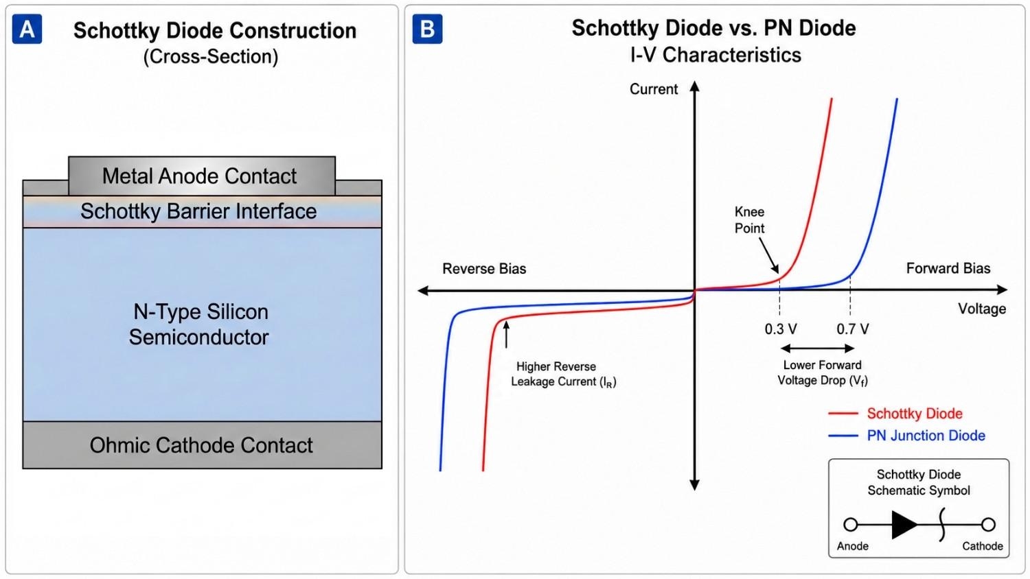
Figure: Schottky diode construction cross-section and comparative I-V curve.
Key Schottky Diode Parameters
- VF (Forward Voltage): Typically ranges from 0.2 V to 0.45 V at lower currents, rising toward 0.5 V to 0.65 V as current nears maximum limits. The popular SS14 Schottky diode (available in an SMA package) exhibits a VF of roughly 0.50 V at its full 1 A rating.
- VRRM (Peak Repetitive Reverse Voltage): The maximum reverse voltage the diode can block continuously. For the SS14, this is rated at 40 V. Running a Schottky diode near or above this limit risks immediate thermal puncture.
- IR (Reverse Leakage Current): Schottky diodes allow significantly more reverse leakage than P-N junction diodes. For example, the SS14 specifies a reverse leakage of 0.2 mA at 25°C, but this figure swells to 6.0 mA at 100°C.
- Reverse Recovery Time (trr): Near-zero. The onsemi 1N5817 datasheet notes majority carrier conduction means the device is not subject to minority carrier reverse recovery transients.
Note
While pure metal-semiconductor junctions have zero trr, commercial Schottky diodes integrate a built-in P-N junction guard ring around their perimeter to suppress edge electric fields and prevent early dielectric breakdown. At very high forward currents, this guard ring can inject minority carriers, creating a small, measurable reverse recovery charge (Qrr) that is typically not captured on standard datasheets when operating above rated forward currents.
Reverse Leakage and Thermal Runaway Risk of Schottky Diode
Because Schottky reverse leakage current is highly sensitive to temperature, it poses a severe thermal runaway risk. As the junction temperature rises, the reverse leakage current increases exponentially. This increased leakage generates more localized power dissipation (calculated as P = Vreverse ✕ IR), which heats the junction further, driving a positive feedback loop.
A 25°C increase in junction temperature can yield a 20x rise in Schottky reverse leakage. Designers must calculate the maximum thermal dissipation using the leakage current at the highest expected operating temperature, rather than relying on standard room-temperature datasheet values.
Zener vs. Schottky Diode Symbol: How to Tell Them Apart
Because Zeners and Schottkys are packaged in identical packages like the SOD-123, their schematic symbols must be carefully audited to prevent PCB layout errors.
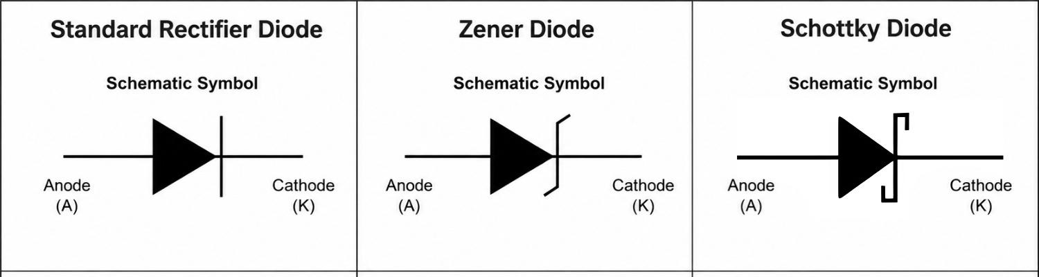
Figure: Comparison of rectifier, Zener, and Schottky schematic symbols.
On physical circuit boards, both components feature a simple painted band to mark the cathode terminal. This makes visual identification impossible once parts are removed from their carrier tapes. When reviewing assembled prototypes, engineers can check the SMD markings printed on the package body.
For assistance identifying specific laser markings, refer to this detailed SMD Diode Code guide to cross-reference common part families.
Zener Diode vs. Schottky Diode: Electrical Characteristics
To understand these differences in a real-world scenario, let us compare the datasheets of two highly popular surface-mount components: a 1N4733A Zener diode and an SS14 Schottky diode.
| Specification | 1N4733A Zener Diode (DO-41 Through-Hole, 1 W) | SS14 Schottky Diode (SMA SMD, 1 A) |
|---|---|---|
| Vz / VF at Rated Current | Vz = 5.1 V at IZT = 49 mA | VF = 0.50 V at IF = 1 A |
| Dynamic Impedance | Zzt = 7 Ohms (at test current) | Not Applicable |
| Temperature Coefficient | TC is roughly -0.01% to +0.04% / °C | VF drops by ~2 mV / °C; IR multiplies 20x per 25°C rise |
| Reverse Leakage Current (IR) | Extremely low (nA range at 25°C) | 0.2 mA at 25°C; climbs to 6.0 mA at 100°C |
| Blocking Capability (VRRM) | N/A (Designed for reverse breakdown) | 40 V |
| Thermal Runaway Risk | Extremely Low | High (Especially at high ambient temperatures) |
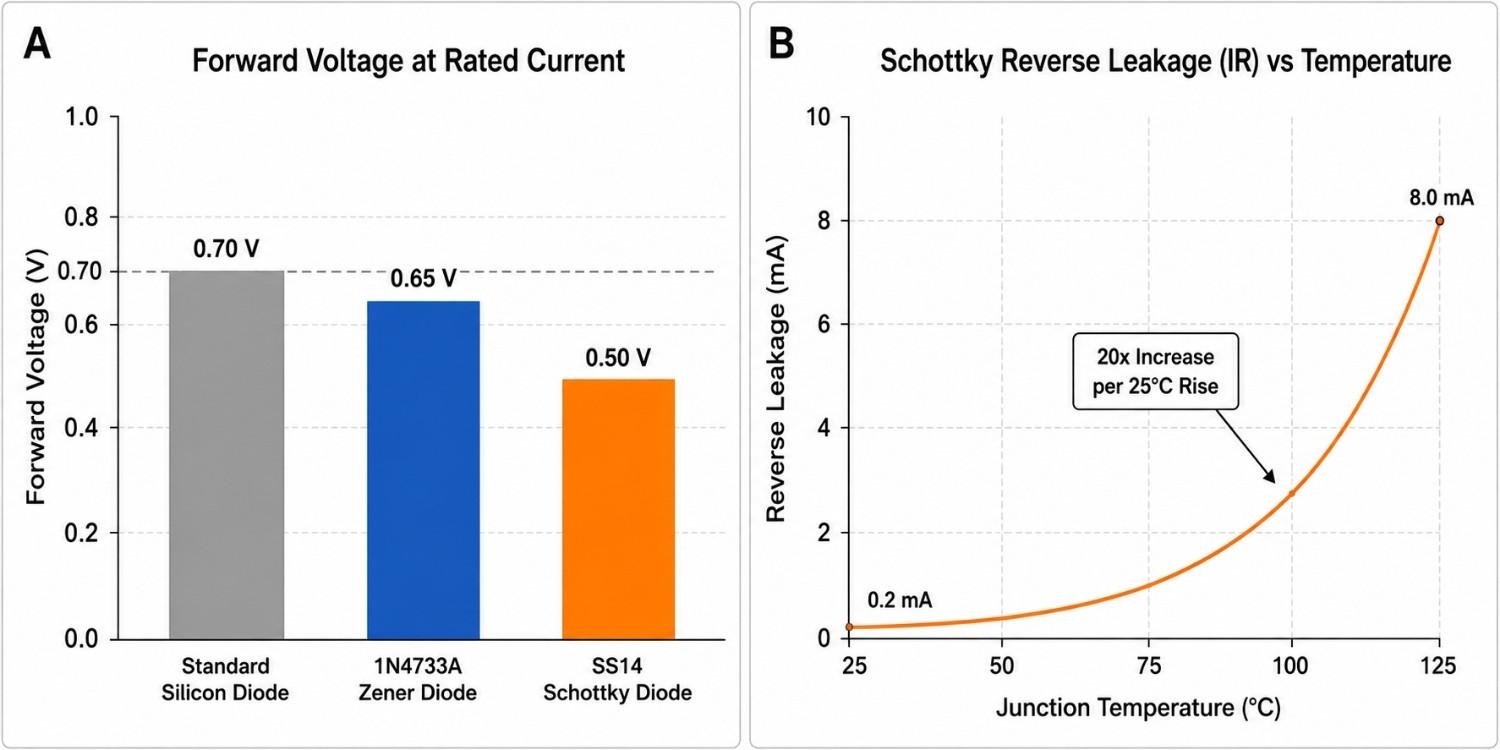
Figure: Charts showing diode forward voltages and Schottky reverse leakage vs temperature.
When to Use a Zener Diode vs Schottky Diode
The operating physics of these two components dictate where they belong on your schematic.
| Circuit Application | Zener Diode | Schottky Diode | Design Notes |
|---|---|---|---|
| Voltage Reference | Yes | No | Schottky forward voltage is highly dependent on current and temperature, making it unsuitable as a reference. |
| MOSFET Gate Protection | Yes | No | Back-to-back Zeners are excellent for protecting sensitive gate-source oxides from static spikes. See details on transistor gate behavior in BJT vs MOSFET comparisons. |
| ADC Signal Clamping | Yes | Limited | A low-voltage Zener prevents analog input pins from exceeding maximum silicon voltage rails. |
| SMPS Freewheeling Path | No | Yes | Schottky's near-zero trr prevents bridge shoot-through and maximizes conversion efficiency. |
| Output Rectifier Stage | No | Yes | Low forward drop minimizes power lost as heat in high-current power stages. |
| Reverse Polarity Protection | No | Yes | Ensure reverse leakage current at maximum operating temperature will not cause thermal runaway. |
| Power Path OR-ing | No | Yes | Ideal for selecting between battery and USB power inputs with negligible voltage drop. |
| RF Signal Detectors | No | Yes | High-speed, majority-carrier switching is required to rectify RF carrier waves. |
| Shunt Voltage Regulation | Yes | No | Only a Zener provides a defined, steep, and repeatable reverse-breakdown voltage. |
| ESD / Surge Protection | No | No | Use dedicated TVS diodes; standard Zeners and Schottkys are either too slow or lack the surge energy handling capabilities. |
Can a Schottky Diode Replace a Zener Diode (or Vice Versa)?
No. Under no circumstances should you swap these components.
- Substituting a Schottky in place of a Zener: A Schottky diode's forward voltage drop is fixed by its metallic junction (~0.3 V to 0.5 V) and cannot be modified. It cannot act as a 5 V or 12 V voltage clamp. If exposed to voltages beyond its peak reverse rating, it will suffer immediate, irreversible breakdown.
- Substituting a Zener in place of a Schottky: Using a Zener as a power rectifier introduces a high forward voltage drop (~0.7 V or higher at power currents), creating significant thermal losses. Additionally, its high reverse recovery time will introduce destructive high-frequency switching noise into your power paths.
Common Pitfalls When Using Schottky Diodes and Zener Diodes
- Neglecting Schottky Leakage in Low-Power Systems: Placing a Schottky diode in a battery-backup power path is excellent for efficiency, but its reverse leakage at 85°C can deplete small coin cells or lithium-polymer batteries unexpectedly fast.
- Ignoring Thermal Impedance in Shunt Regulators: If a load is suddenly disconnected from a shunt regulator, all excess current must pass through the Zener diode. If your layout lacks sufficient heat-sinking copper, the Zener will fail.
- BOM Component Mixing during Pick-and-Place Assembly: Because SOD-123 Zener and Schottky packages look identical on the component reel, double-check your BOM footprint naming. If you are manufacturing high-reliability prototypes, a component mix-up can cause boards to fail initial quality control.
Zener Diode vs Schottky Diode: Package Selection and PCB Layout
The thermal performance and current capacity of your diodes depend heavily on the physical packages you select during layout.
Common Zener Diode Packages
- SOD-323 / SOD-123: Standard for low-power signal Zeners (such as the BZT52 or BZX384 series), offering power ratings between 250 mW and 410 mW.
- SOT-23: Often used for dual-diode arrays, common cathode protection nodes, or precision voltage references (such as the BZX84 family).
- MELF (Metal Electrode Leadless Face): Glass cylindrical packages utilized in high-stability medical or military-grade reference circuits due to their low thermal resistance and resistance to aging.
Common Schottky Diode Packages
- SOD-123: Excellent for low-current signal Schottkys (such as the BAT54 series), typically rated for 200 mA to 300 mA.
- SMA (DO-214AC): The universal footprint for 1 A power Schottky diodes like the SS14.
- SMB (DO-214AA): Step-up package for 2 A to 3 A applications, offering enhanced heat dissipation.
- SMC (DO-214AB): Designed for high-power, high-current environments ranging from 3 A to 5 A.
SMA vs. SMB vs. SMC: Choosing the Right Footprint
For most 1 A power stages, the SMA footprint is the industry default. It balances compact size with pad sizes large enough to solder comfortably. However, if your system operates in ambient temperatures exceeding 70°C, upgrading to an SMB or SMC footprint provides a wider thermal buffer.
To ensure your pad dimensions are perfectly optimized to prevent tombstoning during reflow soldering, consult the comprehensive SMD Diode Size Guide to double-check footprint configurations before locking in your PCB routing.
Thermal and Layout Considerations for PCB Design
- Schottky Heat Dissipation: Extend your cathode copper pour 3 mm to 4 mm beyond the terminal pad on 2 oz copper weight. Because thermal runaway is highly dependent on junction temperature, minimizing the thermal resistance to ambient (Rth_ja) directly prevents runaway conditions.
- Zener Shunt Layout: Size the copper surrounding a shunt Zener to survive worst-case open-load scenarios. When the load drops out, the Zener must handle the entirety of the loop current.
- Visual Verification: Always verify cathode band polarities on your first prototype runs. Swapping orientations during pick-and-place assembly remains one of the most common physical layout errors in rapid turn production.
FAQs about Zener Diode vs Schottky Diode
Q: Can I use a Schottky diode instead of a Zener diode?
No. Schottky diodes have a fixed forward voltage drop determined by their metal-semiconductor junction, meaning they cannot be custom-tuned to clamp at standard voltage limits like 5.1 V or 12 V. Furthermore, they do not possess a stable, non-destructive reverse breakdown region.
Q: Why is a Zener diode not suitable as a high-speed switching rectifier?
Zener diodes are built with heavily doped P-N junctions that store significant minority carrier charges in forward bias. When switched off rapidly, they exhibit a finite, slow reverse recovery time (trr). In switch-mode power supplies, this delay causes severe reverse current spikes and driver failure.
Q: How does temperature affect Schottky diode forward voltage and reverse leakage?
As junction temperature rises, a Schottky diode's forward voltage drop decreases by approximately 2 mV per degree Celsius, which slightly improves conduction efficiency. However, its reverse leakage current increases exponentially, scaling roughly 20x for every 25 degrees Celsius rise, which poses a serious thermal runaway risk.
Q: What makes the 5.6V Zener diode ideal for reference voltage designs?
At approximately 5.6 V, the negative temperature coefficient of the quantum tunneling Zener breakdown exactly cancels out the positive temperature coefficient of the avalanche multiplication breakdown. This results in an exceptionally stable voltage reference with near-zero thermal drift.
Q: Which SMD packages are best suited for high-current Schottky diodes?
For currents of 1 A, SMA (DO-214AC) is the standard selection. For systems running between 2 A and 5 A, larger packages like SMB (DO-214AA) and SMC (DO-214AB) are required. These larger packages provide the copper pad contact area needed to manage thermal dissipation.
Q: Can Zener diodes be used for active rectification?
No. Their high forward voltage drop (0.7 V or higher) and relatively slow reverse recovery times make Zeners highly inefficient for standard rectification tasks, leading to excessive heat generation.
Conclusion
When selecting between a Zener and a Schottky diode, remember this simple rule: if your circuit needs to regulate or clamp a voltage, choose a Zener diode; if your circuit needs to pass current with minimal power loss, choose a Schottky diode.
Always cross-reference your operating temperatures, peak currents, and package thermal resistance on actual component datasheets. Taking the time to verify these parameters during the design stage ensures your PCB performs reliably under real-world operating conditions.
Before finalizing your design files, check component availability in the JLCPCB Parts Library and get an instant quote!
Popular Articles
• SMD Capacitor Sizes: Complete Size Chart and Selection Tips for PCB Design and Assembly
• SMD Diode Code Lookup: Full List, Marking Guide & Identification [2026 Guide]
• SMD Resistor Package Sizes: Complete Size Chart, Footprints & How to Choose
• SMD Capacitor Codes: Identification, Markings, and Polarity
• How to Solder SMD Components Like a Pro [2026 Updated]
Keep Learning
What Is the ESP32? A Complete Guide to Features, Architecture, Modules, Programming, and Applications
From Wi-Fi-enabled temperature sensors and wearable health monitors to industrial gateways and AI-powered cameras, the ESP32 microcontroller has become one of the world's most widely adopted wireless embedded platforms. Combining a powerful processor with integrated Wi-Fi and Bluetooth, it lets engineers build connected devices without separate networking hardware. This guide covers ESP32 specifications, architecture, the full family of variants, development boards, programming tools, and real-world E......
How to Choose the Right STM32 Microcontroller: Compare Series, Cortex-M Cores, and Key Features
STMicroelectronics ships thousands of STM32 MCU part numbers across more than a dozen series, and that variety is exactly what makes STM32 microcontroller selection difficult. Pick the wrong family, and you pay for it later: oversized BOM cost, wasted power budget, or a board respin when a peripheral turns out to be missing. This STM32 microcontroller selection guide breaks the decision into a five-step framework built on practical engineering criteria, not datasheet marketing copy, so you can match a......
SMD Transistor Code Lookup: Identify Markings, Pinout & Multimeter Test Guide
Repairing a circuit board often brings a familiar frustration: staring at a tiny, three-legged black component with an obscure two- or three-letter code. Whether troubleshooting a bare prototype or a mass-produced PCBA, knowing how to quickly decode these surface-mount device (SMD) markings is an essential skill for any electronics engineer or repair technician. In this comprehensive guide, you will learn: 1. How to decode SMD transistor marking codes 2. How to identify BJT vs MOSFET types 3. How to f......
SMD Capacitor Sizes: Complete Size Chart and Selection Tips for PCB Design and Assembly
In the world of modern electronics, surface mount devices (SMDs) have revolutionized board design, allowing for smaller, faster, and more efficient printed circuit boards. When designing a PCB, selecting the correct SMD capacitor sizes is one of the most critical decisions an engineer must make to ensure both electrical reliability and manufacturability. In this article, you will find practical, authoritative guidance on: Comprehensive SMD capacitor size charts for quick reference. How to read imperia......
SMD Diode Code Lookup: Full List, Marking Guide & Identification [2026 Guide]
In modern electronics, surface-mount diodes are used everywhere - from power input protection circuits to high-speed signal routing. Because these components are extremely small, manufacturers cannot print full part numbers on their bodies. Instead, they use short marking codes such as A2, M7, SS14, or SL, which often confuse beginners during PCB repair, reverse engineering, or component replacement. This guide explains how to decode SMD diode codes, identify polarity, test components using a multimet......
Thin Film vs. Thick Film Resistors: Key Differences & Selection Guide
Key Takeaways Default to thick film resistors for most designs. They are cost-effective, robust, and ideal for pull-ups, LED current-limiting, digital circuits, and surge-prone applications. Choose thin-film resistors whenever a resistor defines an analog quantity, such as a voltage divider, reference network, gain-setting circuit, or current-sensing signal chain. Their tight tolerance and low TCR help maintain measurement accuracy over temperature and time. Most PCB designs use thick film or thin fil......