
Complete SMD Diode Size Guide: Package Dimensions, Charts, and Selection Tips
14 min
- Understanding SMD Diode Package Naming
- SMD Diode Size Chart
- Common SMD Diode Package Sizes
- Choosing the Right SMD Diode Package
- Common Mistakes When Selecting SMD Diode Sizes
- PCB Design Guidelines for SMD Diode Packages
- Why SMD Diode Package Size Matters
- How SMD Diode Package Size Affects Current and Thermal Performance
- FAQs about SMD Diode Size
- Conclusion
Picking the wrong SMD diode package usually shows up late, either during layout when footprints mismatch, or during testing when junction heating climbs past safe limits. Package size dictates how much current a diode carries, how efficiently it sheds heat, and whether your assembly line can solder it reliably.
This guide details common SMD diode package families (SMA, SMB, SMC, SOD-123, SOD-323, SOD-523, and SOD-923).
You will find our comprehensive SMD diode package size chart, layout recommendations, and a practical selection guide by application.
Understanding SMD Diode Package Naming
Before jumping into the SMD diode dimensions, decoding the standard naming conventions prevents footprint mismatches. Understanding these names is also a helpful foundation when reviewing SMD transistor codes or selecting IC package types for your broader design.
SMA, SMB, and SMC
These are JEDEC-standardized designations for surface-mount power diodes in the DO-214 family. The letters indicate size increments within the series. SMA is the smallest, and SMC is the largest. Their formal JEDEC names are DO-214AC (SMA), DO-214AA (SMB), and DO-214AB (SMC).
SOD-123, SOD-323, SOD-523 and SOD-923
SOD stands for Small Outline Diode. Within the common SOD series discussed here, higher numbers generally correspond to smaller package sizes. SOD-123 is the largest, followed by the highly compact SOD-323, SOD-523, and SOD-923. These flat, two-terminal packages are designed primarily for signal and low-power rectifier applications.
JEDEC Package Standards
JEDEC (Joint Electron Device Engineering Council) is the standards body responsible for semiconductor package specifications. Following JEDEC-compliant footprints in your PCB layout reduces the risk of physical component mismatches. Checking standard diode symbols in your schematic capture tool against the JEDEC footprint is a highly recommended verification step.
SMD Diode Size Chart
If you need immediate dimensional data, use the SMD diode size chart below. It compares the most common packages by footprint, current capacity, and typical use cases.
| Package | Nominal Body Dimensions (mm) | Max Continuous Current | Power Dissipation (PCB) | Approx. Area | Typical Applications |
|---|---|---|---|---|---|
| SMA (DO-214AC) | 4.4 x 2.7 x 2.3 | 1 A | 1 W (up to 2 W w/ copper) | ~24 mm² | General rectifiers, low-power TVS |
| SMB (DO-214AA) | 5.6 x 3.8 x 2.4 | 2 A | 1.5 W (up to 2.5 W) | ~40 mm² | Medium rectifiers, interface TVS |
| SMC (DO-214AB) | 7.7 x 5.9 x 2.6 | 3-5 A | 2-3.5 W (up to 5+ W) | ~75 mm² | High-power rectifiers, surge TVS |
| SOD-123 | 2.8 x 1.8 x 1.2 | 200-500 mA | 350-500 mW | ~9 mm² | ESD data lines, small signal |
| SOD-323 | 1.7 x 1.25 x 0.9 | 200-300 mA | 200-350 mW | ~4 mm² | Mobile ESD, compact rectifiers |
| SOD-523 | 1.2 x 0.8 x 0.6 | 150-250 mA | 150-250 mW | ~1.3 mm2 | Logic boards, compact portables |
| SOD-923 | 1.0 x 0.5 x 0.5 | ≤ 200 mA | 100-150 mW | ~1 mm² | Wearables, IoT devices |
| D2PAK (TO-263) | 10.2 x 8.9 x 4.6 | 10-30+ A | 20-30+ W w/ heatsink | ~180 mm² | SMPS rectifiers, motor drives |
Note
Dimensions listed above and throughout this guide are common nominal package sizes. Exact measurements and tolerances may vary slightly between manufacturers and specific JEDEC variants. Always verify against your specific component's datasheet.
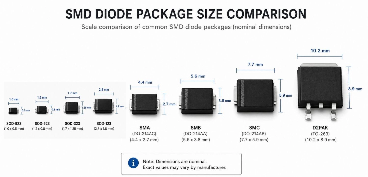
Figure: Common SMD diode packages showing nominal dimensions.
Common SMD Diode Package Sizes
The following sections break down exactly when and why you should choose each specific footprint.
SMA Package (DO-214AC)
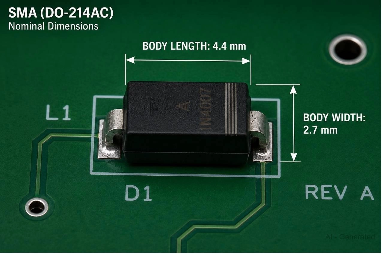
Figure: SMA DO-214AC SMD diode showing nominal 4.4 x 2.7 mm dimensions.
Quick Specs & Recommendations:
- Nominal Dimensions: 4.4 x 2.7 x 2.3 mm
- Max Current: 1 A continuous
- Power Dissipation: 1 W standard footprint
- Best Applications: General-purpose rectifiers, battery protection Schottky diodes, and industrial signal lines.
- Recommendation: The industry standard for basic power handling. Offers an excellent balance of manageable board area and reliable manual solderability.
SMB Package (DO-214AA)
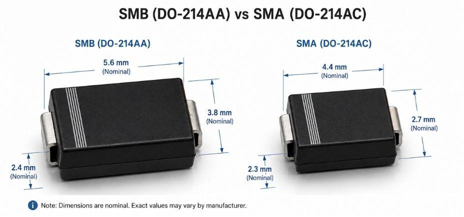
Figure: Size comparison of SMB and SMA diode packages showing nominal dimensions.
Quick Specs & Recommendations:
- Nominal Dimensions: 5.6 x 3.8 x 2.4 mm
- Max Current: 2 A continuous
- Power Dissipation: 1.5 W standard footprint
- Best Applications: Medium-power rectifiers, flyback diodes across relay coils, and moderate TVS ESD protection.
- Recommendation: Choose SMB when an SMA package falls slightly short on current, but an SMC package would waste board space.
SMC Package (DO-214AB)
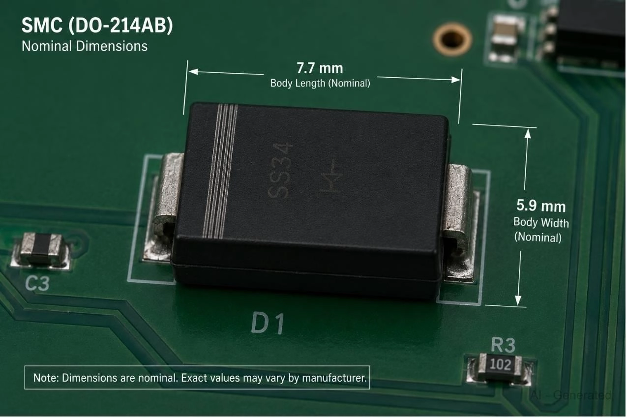
Figure: SMC DO-214AB power diode showing nominal 7.7 x 5.9 mm dimensions on a PCB.
Quick Specs & Recommendations:
- Nominal Dimensions: 7.7 x 5.9 x 2.6 mm
- Max Current: 3-5 A continuous
- Power Dissipation: 2-3.5 W standard footprint
- Best Applications: SMPS output stages, automotive reverse battery protection, and high-energy surge clamping.
- Recommendation: Best for heavy-duty power line clamping and substantial continuous current requirements.
SOD-123 Package
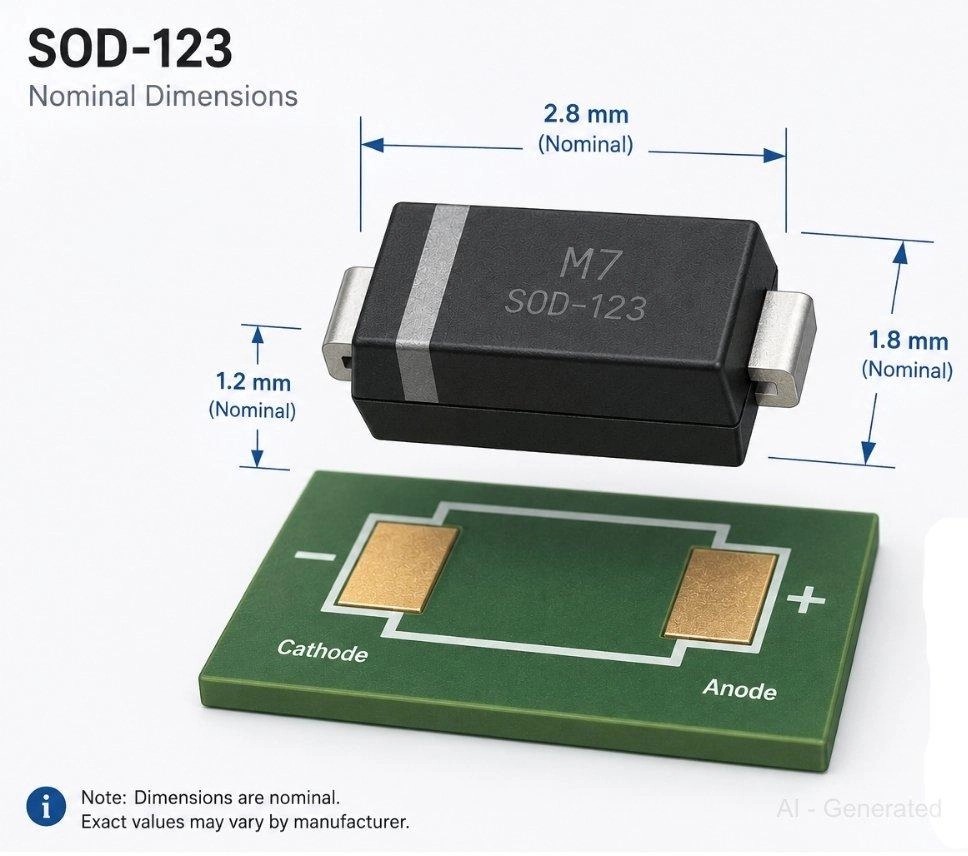
Figure: SOD-123 dimensions 2.8 x 1.8 mm
Quick Specs & Recommendations:
- Nominal Dimensions: 2.8 x 1.8 x 1.2 mm
- Max Current: 200-500 mA continuous
- Power Dissipation: 350-500 mW standard footprint
- Best Applications: Low-power Schottky rectifiers, signal clipping, and USB/HDMI ESD protection.
- Recommendation: The go-to choice for logic-level signals. Small enough for dense layouts but still practical for manual prototyping.
SOD-523 Package
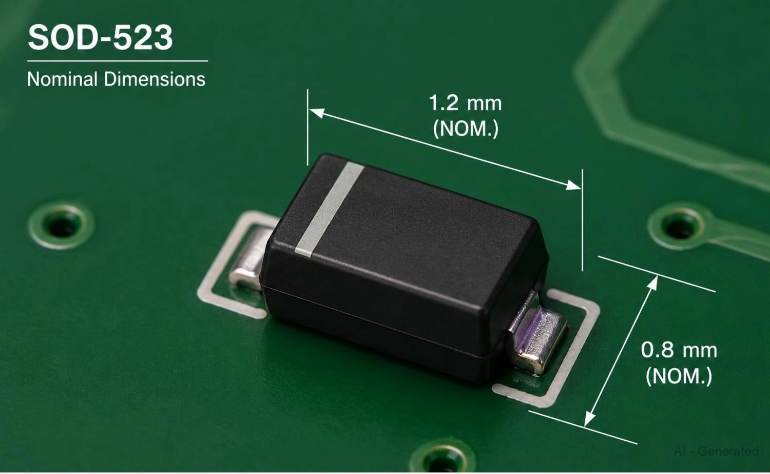
Figure: SOD-523 package dimensions 1.2 x 0.8 mm.
Quick Specs & Recommendations:
- Nominal Dimensions: 1.2 x 0.8 x 0.6 mm
- Max Current: 150-250 mA continuous
- Power Dissipation: 150-250 mW standard footprint
- Best Applications: High-density logic boards, LED drivers, and compact portable electronics.
- Recommendation: Offers an excellent middle ground between the SOD-323 and the ultra-tiny SOD-923. It is roughly equivalent to a 0603 footprint, requiring pick-and-place assembly.
SOD-323 Package Dimensions
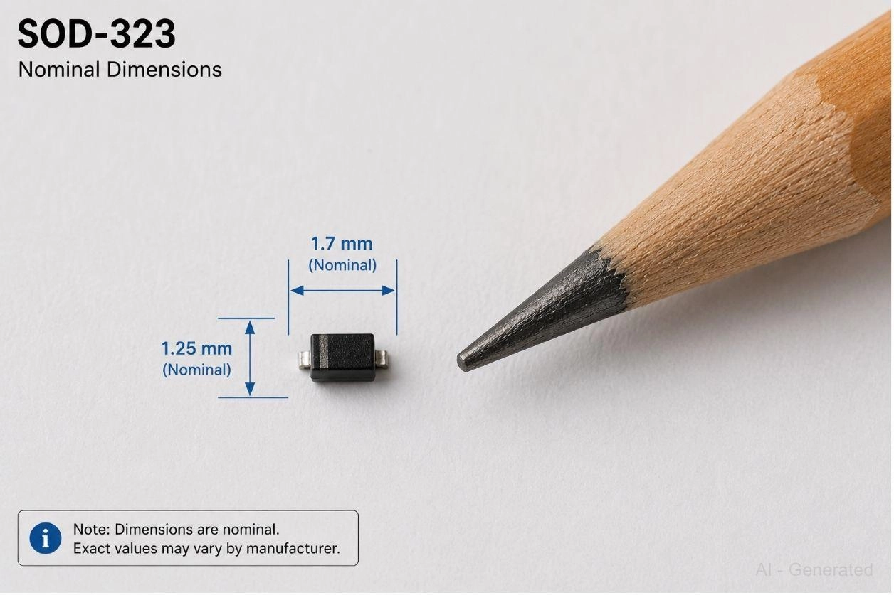
Figure: SOD-323 dimensions 1.7 x 1.25 mm
Quick Specs & Recommendations:
- Nominal Dimensions: 1.7 x 1.25 x 0.9 mm
- Max Current: 200-300 mA continuous
- Power Dissipation: 200-350 mW standard footprint
- Best Applications: Portable device reverse polarity protection, switch-mode rectification, and RF circuits.
- Recommendation: Ideal for lightweight consumer electronics. Reflow assembly is highly recommended due to the miniature pad pitch.
SOD-923 Package
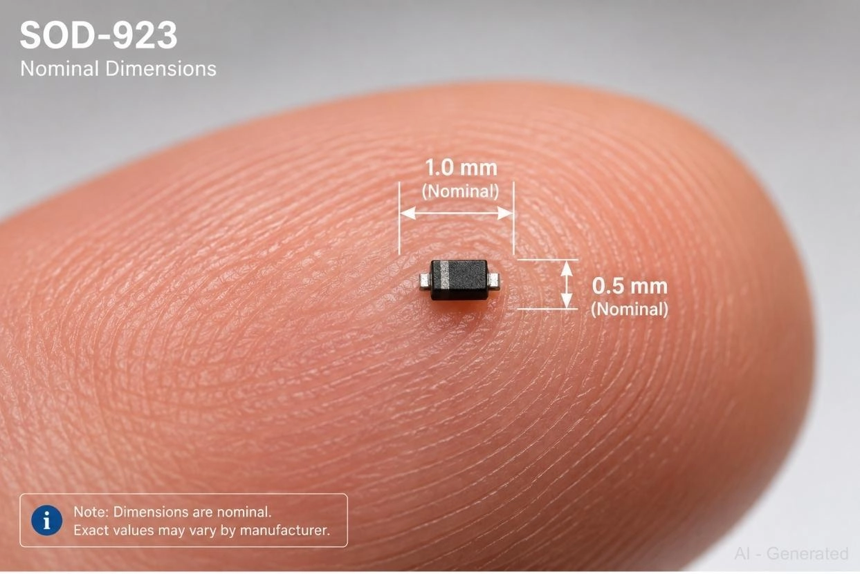
Figure: Ultra-miniature nominal 1.0 x 0.5 mm SOD-923 SMD diode.
Quick Specs & Recommendations:
- Nominal Dimensions: 1.0 x 0.5 x 0.5 mm
- Max Current: ≤ 200 mA continuous
- Power Dissipation: 100-150 mW standard footprint
- Best Applications: Wearable electronics, smartphones, and ultra-compact RF modules.
- Recommendation: Best for high-density applications where board space is critical. Requires automated pick-and-place assembly.
D2PAK Package
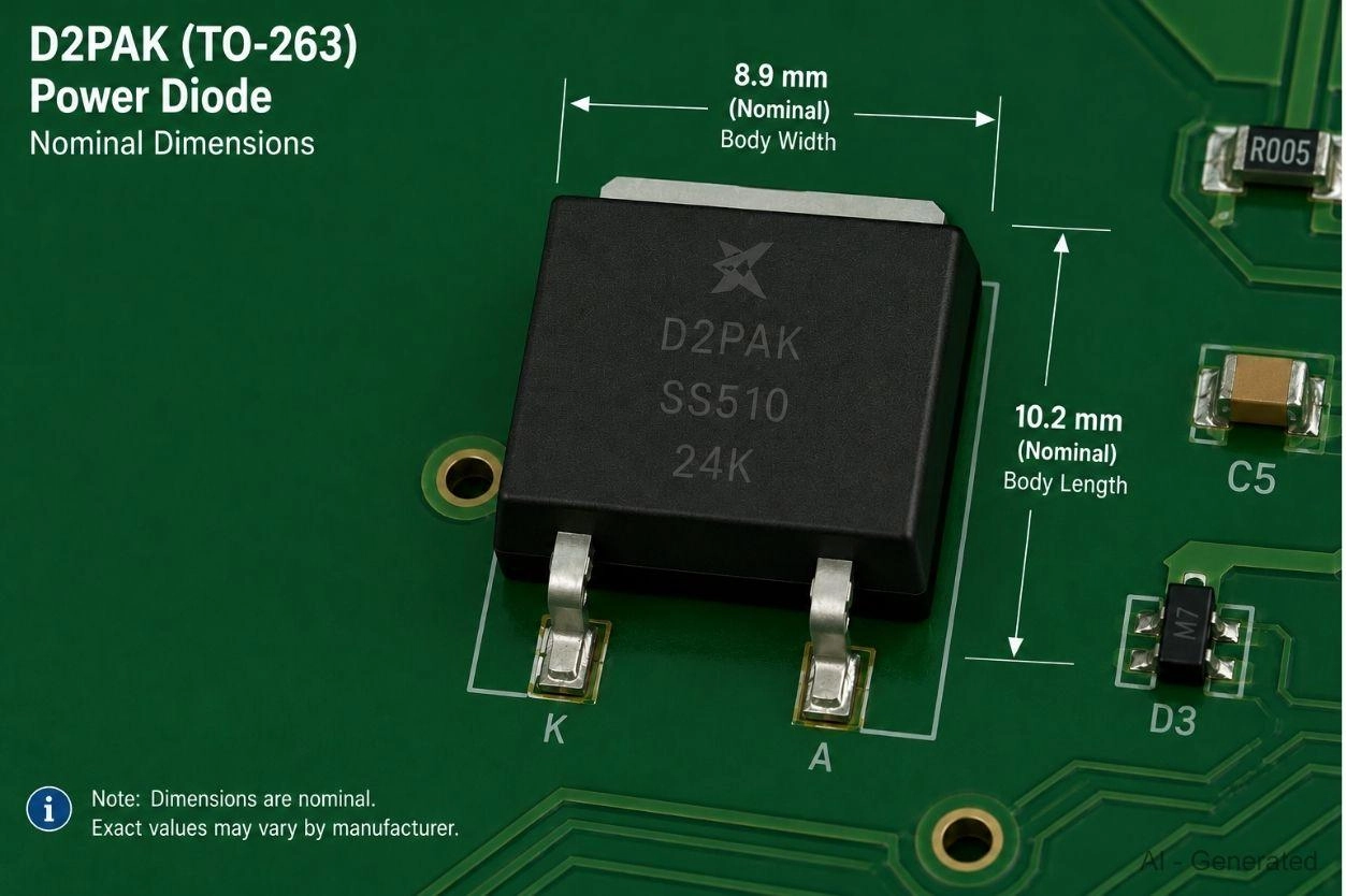
Figure: D2PAK TO-263 power diode showing nominal 10.2 x 8.9 mm dimensions on a PCB.
Quick Specs & Recommendations:
- Nominal Dimensions: 10.2 x 8.9 x 4.6 mm
- Max Current: 10-30+ A continuous
- Power Dissipation: 20-30+ W with heavy copper/heatsinking
- Best Applications: Synchronous rectification, motor drive freewheeling diodes, and high-power SMPS.
- Recommendation: Well-suited for high-current power stages and thermally demanding designs.
Choosing the Right SMD Diode Package
Use these practical guidelines to narrow down your choices based on your application.
For High-Frequency SMPS Designs
Switching power supplies operating above 100 kHz demand fast recovery or Schottky diodes.
- Low power: SOD-323, SOD-123
- Medium power (5-30 W): SMA, SMB
- High power (>50 W): SMC, D2PAK
For TVS and Surge Protection
TVS diode selection hinges on peak pulse power.
- Basic ESD (USB/signal lines): SOD-123, SOD-323
- Heavy Surge (AC mains/Automotive): SMC packages for robust load-dump protection
For Compact IoT and Mobile Devices
IoT designs prioritize size and power consumption over current capacity.
- Recommended Packages: SOD-923, SOD-523, SOD-323
- Design Note: Keep total continuous current under 100 mA to avoid thermal throttling inside enclosed plastic housings.
For Automotive and Industrial Electronics
Automotive designs must survive wide temperature swings (-40°C to +125°C) and heavy vibration.
- Recommended Packages: SMB, SMC
- Design Note: These packages provide the necessary vibration resistance and thermal headroom for harsh environments.
Common Mistakes When Selecting SMD Diode Sizes
Watch out for these frequent errors when reviewing your designs.
Choosing an Undersized SMD Diode Package
When sourcing electronic parts, do not select a diode based purely on average continuous current. A 1A SMA diode can easily be destroyed by a 5A startup inrush spike if the repetitive peak rating is exceeded.
Ignoring Thermal Derating
A diode rated for 1 A at 25°C ambient may only be safe to push 600 mA at 70°C. The ambient temperature inside an enclosure is often much higher than room temperature. Always check the thermal derating chart.
Poor PCB Copper Heatsinking
Adding a package to a board with minimum-width traces limits cooling capacity. For any package dissipating more than a few hundred milliwatts, the pad copper area should be extended.
Using Ultra-Small Packages for Manual Assembly
Trying to hand-build prototype boards with SOD-923 parts leads to ruined components and invisible shorts. Specify SOD-123 as the minimum acceptable package size for manual diode soldering.
PCB Design Guidelines for SMD Diode Packages
Smaller packages such as SOD-323, SOD-523, and SOD-923 require tighter stencil and solder paste control than larger SMA or SMB packages.

- For production builds, professional PCB assembly services such as JLCPCB help maintain consistent placement accuracy across fine-pitch SMD diode footprints.
SMD Diode Footprint Spacing and Reflow Soldering
Following JEDEC-recommended land patterns and proper solder pad design is critical for reliable SMD diode assembly. Incorrect pad sizing can cause tombstoning, poor solder wetting, or diode misalignment during reflow.
Thermal Copper Area for SMD Diode Packages
SMD diode thermal performance depends heavily on PCB copper area. Extending copper pours around SMA, SMB, SMC, and D2PAK packages significantly improves heat spreading and reduces junction temperature.
For higher-power diode packages:
- Use wider copper pours around the anode and cathode.
- Connect thermal pads to internal planes.
- Add thermal vias beneath D2PAK packages.
This becomes especially important in SMPS, automotive, and surge-protection circuits where continuous current and transient power are high.
Manual Soldering vs PCB Assembly for Small SMD Diodes
Ultra-small diode packages like SOD-923 and SOD-523 are extremely difficult to solder manually due to their tiny pad geometry and limited spacing. Even SOD-323 packages can become challenging without magnification and fine-tip tools.
For prototype or production boards using miniature SMD diode packages, automated SMT assembly through services like JLCPCB provides much more reliable solder consistency and placement accuracy.
For hand assembly, the most practical choices remain:
- SMA
- SMB
- SOD-123
PCB Clearance Requirements for High-Voltage SMD Diodes
High-voltage SMD diode layouts require proper creepage and clearance spacing between pads, copper pours, and adjacent traces.
Packages such as SMB and SMC are commonly used in:
- AC mains rectification
- TVS surge suppression
- Industrial flyback protection
When working above 400 V, always follow IPC-2221 spacing recommendations, even if compact package placement appears electrically possible.
Why SMD Diode Package Size Matters
Choosing a package is not purely about fitting a component onto a board. Package size affects far more than physical dimensions, directly determining how the device behaves under load and how straightforward it is to manufacture.
- PCB Space and Compact Circuit Design: Modern electronics, particularly IoT sensors and wearables, operate under tight area constraints. A SOD-923 measures roughly 1.0 x 0.5 mm, making it practical for dense layouts where an SMA package simply will not fit. However, minimizing package size without considering heat dissipation can cause major reliability issues.
- Current Handling and Cooling Performance: Larger packages feature lower junction-to-ambient thermal resistance (θJA). This allows heat to escape more efficiently, so the diode can carry more current before hitting its maximum rated temperature limit. For example, an SMA diode can handle 1A continuous forward current, while a SOD-923 is often limited to 200 mA or less.
- Package Size vs. Power Dissipation: Power dissipation (PD) is calculated simply: PD = VF x IF. Smaller packages force more heat to stay in the junction. As ambient temperature rises, the maximum safe power dissipation drops significantly, which is critical for enclosed or elevated-temperature environments.
- Manufacturing and Soldering Considerations: Package size dictates your assembly method. Ultra-small packages like SOD-923 require pick-and-place machines; hand-soldering them is extremely difficult. Conversely, larger packages like SMA and SMC are easily managed for manual prototyping and low-volume production.
How SMD Diode Package Size Affects Current and Thermal Performance
Understanding how heat dissipation connects to physical size prevents real-world failures.
How SMD Diode Package Size Affects Current Handling
The maximum current a diode can sustain without damage is limited by junction heating. As forward current increases, power dissipation raises the junction temperature. Larger packages offer lower thermal resistance, allowing more power to escape before the junction overheats.
PCB Copper Area and Thermal Dissipation
Datasheets publish values assuming a minimal footprint on a standard board. Adding robust copper pours around your diode improves heat spreading dramatically. Adding one square centimeter of 1 oz copper reduces thermal resistance by roughly 30-50°C/W as a general estimate, though this depends heavily on layer count and copper thickness. Both the anode and cathode pads contribute to cooling.
Surge Power Capability and Package Size
Larger packages tolerate transient energy spikes much better. An SMC-packaged TVS diode might absorb a peak pulse of 1500 W, while a SOD-123 is typically limited to 100-200 W. Always match package size to your expected surge environment.
FAQs about SMD Diode Size
Q: What is the most common SMD diode package?
SOD-123 handles low-power logic and consumer electronics, while SMA is the default for general power handling and industrial rectifiers.
Q: What is the difference between SMA and SMB packages?
SMB is physically larger (5.6 x 3.8 mm vs. 4.4 x 2.7 mm) and supports roughly double the continuous current (2 A vs. 1 A). Use SMB when an SMA package runs too hot for your load.
Q: Can I replace a through-hole diode with an SMD equivalent?
Yes. SMA is the standard SMD replacement for DO-41 diodes (like the 1N4007), while SMB replaces the larger DO-15. Ensure your PCB has adequate copper pours to replace the cooling effect of the original wire leads.
Q: Why do some SMD diodes come in 3-pin packages?
Packages like SOT-23 often contain two separate diodes wired internally (e.g., in series or common cathode). This saves valuable board space when designing logic gates or redundant power inputs.
Q: How do I identify an unknown SMD diode package?
Measure the body length and width with calipers. Compare your measurements against a standard SMD diode package size chart. If a laser marking is visible, check it against an online SMD code database.
Conclusion
Selecting the right SMD diode package comes down to balancing current demands, thermal limits, available board space, and layout constraints.
When in doubt, prioritize thermal margin over a minimum footprint. Always verify package thermal behavior experimentally under real PCB copper conditions, as minimum-pad datasheet values rarely reflect enclosed environments.
Once your design constraints are met, validate your JEDEC footprints before moving to production. Transitioning to prototype PCB assembly with JLCPCB provides a straightforward way to ensure your footprint choices and thermal assumptions perform reliably in the real world.
Popular Articles
• SMD Capacitor Sizes: Complete Size Chart and Selection Tips for PCB Design and Assembly
• SMD Diode Code Lookup: Full List, Marking Guide & Identification [2026 Guide]
• SMD Resistor Package Sizes: Complete Size Chart, Footprints & How to Choose
• SMD Capacitor Codes: Identification, Markings, and Polarity
• How to Solder SMD Components Like a Pro [2026 Updated]
Keep Learning
What Is the ESP32? A Complete Guide to Features, Architecture, Modules, Programming, and Applications
From Wi-Fi-enabled temperature sensors and wearable health monitors to industrial gateways and AI-powered cameras, the ESP32 microcontroller has become one of the world's most widely adopted wireless embedded platforms. Combining a powerful processor with integrated Wi-Fi and Bluetooth, it lets engineers build connected devices without separate networking hardware. This guide covers ESP32 specifications, architecture, the full family of variants, development boards, programming tools, and real-world E......
How to Choose the Right STM32 Microcontroller: Compare Series, Cortex-M Cores, and Key Features
STMicroelectronics ships thousands of STM32 MCU part numbers across more than a dozen series, and that variety is exactly what makes STM32 microcontroller selection difficult. Pick the wrong family, and you pay for it later: oversized BOM cost, wasted power budget, or a board respin when a peripheral turns out to be missing. This STM32 microcontroller selection guide breaks the decision into a five-step framework built on practical engineering criteria, not datasheet marketing copy, so you can match a......
SMD Transistor Code Lookup: Identify Markings, Pinout & Multimeter Test Guide
Repairing a circuit board often brings a familiar frustration: staring at a tiny, three-legged black component with an obscure two- or three-letter code. Whether troubleshooting a bare prototype or a mass-produced PCBA, knowing how to quickly decode these surface-mount device (SMD) markings is an essential skill for any electronics engineer or repair technician. In this comprehensive guide, you will learn: 1. How to decode SMD transistor marking codes 2. How to identify BJT vs MOSFET types 3. How to f......
SMD Capacitor Sizes: Complete Size Chart and Selection Tips for PCB Design and Assembly
In the world of modern electronics, surface mount devices (SMDs) have revolutionized board design, allowing for smaller, faster, and more efficient printed circuit boards. When designing a PCB, selecting the correct SMD capacitor sizes is one of the most critical decisions an engineer must make to ensure both electrical reliability and manufacturability. In this article, you will find practical, authoritative guidance on: Comprehensive SMD capacitor size charts for quick reference. How to read imperia......
SMD Diode Code Lookup: Full List, Marking Guide & Identification [2026 Guide]
In modern electronics, surface-mount diodes are used everywhere - from power input protection circuits to high-speed signal routing. Because these components are extremely small, manufacturers cannot print full part numbers on their bodies. Instead, they use short marking codes such as A2, M7, SS14, or SL, which often confuse beginners during PCB repair, reverse engineering, or component replacement. This guide explains how to decode SMD diode codes, identify polarity, test components using a multimet......
Thin Film vs. Thick Film Resistors: Key Differences & Selection Guide
Key Takeaways Default to thick film resistors for most designs. They are cost-effective, robust, and ideal for pull-ups, LED current-limiting, digital circuits, and surge-prone applications. Choose thin-film resistors whenever a resistor defines an analog quantity, such as a voltage divider, reference network, gain-setting circuit, or current-sensing signal chain. Their tight tolerance and low TCR help maintain measurement accuracy over temperature and time. Most PCB designs use thick film or thin fil......