Voltage Regulator PCB: Practical Design Guide
19 min
- Introduction
- How a Voltage Regulator Works on a PCB
- Voltage Regulator PCB Diagram and Schematic
- Voltage Regulator PCB Design for 12V Applications
- Voltage Regulator PCB Layout Best Practices
- Key Components in a Voltage Regulator Circuit
- Common Voltage Regulator PCB Design Mistakes
- FAQs about Voltage Regulator PCB
- Conclusion About Voltage Regulator PCB
Key Takeaways
A voltage regulator PCB doesn't just convert one voltage into another; it must also provide a stable output while handling heat, load changes, and noise in the circuit.
The layout is as important as the regulator IC; keep the input and output capacitors near the pins, use short power connections, and ensure a direct, low-impedance ground return.
Linear regulators are simple and quiet, but they lose voltage difference as heat; switching regulators are the better option when the voltage drops or the load current is high.
The input and output capacitors belong to the regulator system and are not optional decoration; their values, types, and, in some cases, their ESR must comply with the regulator's datasheet.
When designing with a 12 V supply, calculate power dissipation before routing the board, since a circuit that is electrically correct may still fail if the regulator cannot dissipate the heat.
Before routing a 12 V design, use the quick-selection table in the thermal design section to check whether your voltage and current combination suits a linear regulator or calls for a heatsink or a buck converter.
Introduction
A prototype may look perfect on the bench but become unstable when you connect a load; the output might sag, the regulator might get so hot it is impossible to touch, or a microcontroller might reset every time a motor starts. In most cases, the regulator isn't the real cause; the voltage regulator's PCB layout is.
Designing a good regulator starts with the right circuit, but it doesn't stop with the schematic. Trace resistance, capacitor placement, copper area, ground return paths, and package temperature all affect the outcome. This guide explains how a voltage regulator works on a PCB, shows how a typical schematic becomes a two-layer PCB, covers common 12 V to 5 V and 12 V to 3.3 V designs, and provides practical layout and thermal rules you can use on real boards.
The aim is not to turn each power supply into a complex power-electronics project; rather, it is to identify which factors matter so that a simple regulator functions as a reliable component of the power supply rather than becoming a weak point.
How a Voltage Regulator Works on a PCB
A voltage regulator keeps the output voltage close to the desired value even when the input voltage or load current varies within its operating range. On a printed circuit board, the regulator works with its input capacitor, output capacitor, copper connections, and ground path. The two usual methods are linear regulation and switching regulation.
Linear Regulators
A linear regulator functions as a controlled series component and constantly varies its internal conduction so that the output remains at the desired voltage. Its main advantage is simplicity, since it requires only a small number of external components and generates very little switching noise. The disadvantage is heat, as the regulator dissipates excess voltage. A useful first estimate is:

Switching Regulators
A switching regulator rapidly stores and transfers energy using components such as an inductor, a diode, or synchronous MOSFETs as well as capacitors. While this gives it much higher efficiency, especially with large voltage or current differences, it also makes PCB layout more critical because high-frequency current loops can cause ripple and EMI. The article mainly focuses on linear regulator layout; switching power stages must follow their own loop-area and EMI rules.
Voltage Regulator PCB Diagram and Schematic
A voltage regulator PCB design starts with an electrical schematic, which shows how components connect, while the PCB layout shows how those connections behave physically. Both views are necessary because a circuit that is correct on paper may perform poorly if long, thin, or poorly placed copper traces connect the same nodes.
Voltage Regulator Circuit Schematic
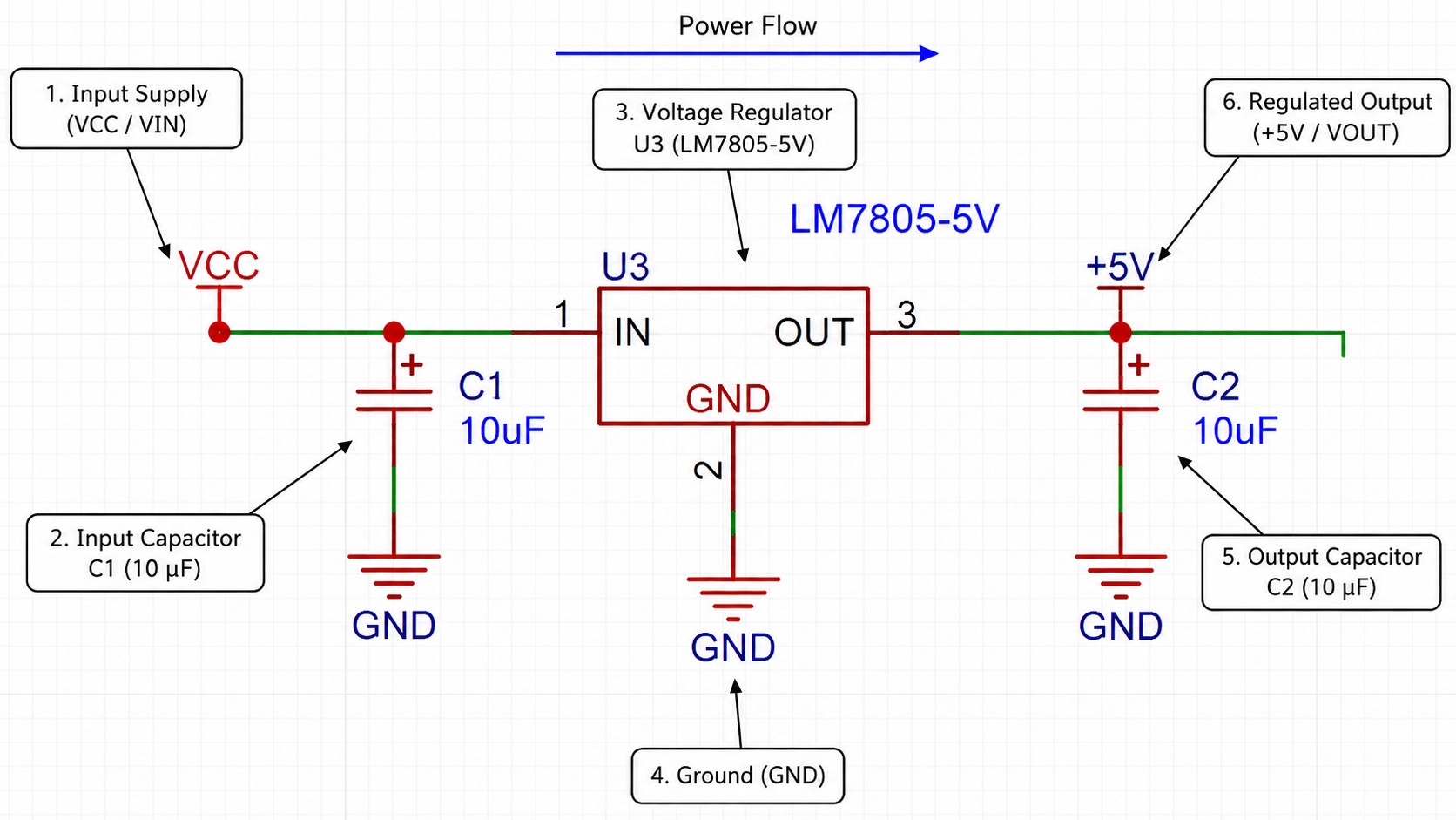
Figure 1. Circuit schematic diagram of an LM7805 voltage regulator with input and output filtering capacitors connected between VCC, VOUT, and ground.
A typical PCB diagram for a voltage regulator follows this sequence: input supply, input capacitor, regulator IC, output capacitor, and finally the load. For example, if you use a 7805 or a similar fixed linear regulator, connect the input capacitor between VIN and ground, and the output capacitor between VOUT and ground.
The input capacitor provides short-term current locally and removes high-frequency noise that might enter via the power cable or from the upstream supply. The output capacitor helps the regulator stay stable during load changes and reduces output ripple and transient variation. The exact values vary by application; For a 7805-type regulator, datasheets typically specify an input bypass of about 0.33 µF when the device is far from the main supply filter, along with a 0.1 µF ceramic at the output; the 10 µF capacitors shown in Figures 1 and 3 also work well and additionally cover long supply leads, whereas many LDOs require larger output capacitance—typically 10 µF or more—and may specify an ESR range. Always rely on the regulator datasheet for the final decision.
A reverse-protection diode is also useful if the output may remain charged while the input suddenly fails. Rather than letting reverse current pass through a regulator that can't withstand it, it provides a safer path for stored output energy.
From Schematic to PCB Layout
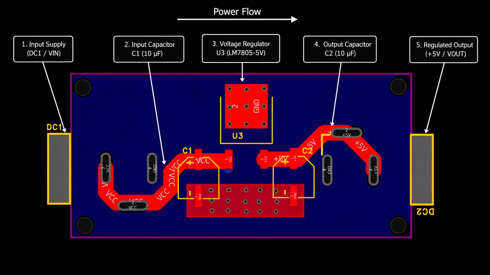
Figure 2. Printed circuit board layout showing top-layer copper routing and component placement for an LM7805 voltage regulator circuit.
Once the schematic is complete, assign a physical footprint to each symbol and place it on the PCB. What is important is not visual symmetry but electrical distance. Place the input capacitor next to the VIN and ground pins, and the output capacitor next to the VOUT and ground pins. This keeps the current paths short and reduces both trace resistance and parasitic inductance.
On a two-layer board, you can route most components on one layer while the other layer maintains a large, continuous ground plane. Size power traces according to the current they carry, rather than giving them the same narrow width as signal traces. The layout must make it easy to follow the main current from the connector through to the regulator and then to the load.
Voltage Regulator PCB Design for 12V Applications
Twelve-volt input is common in automotive electronics, industrial controls, adapters, battery-backed systems, and do-it-yourself equipment, and it also highlights the thermal limits of linear regulators, especially when the required output is 5 volts or 3.3 volts.
Common 12V Regulator Circuits
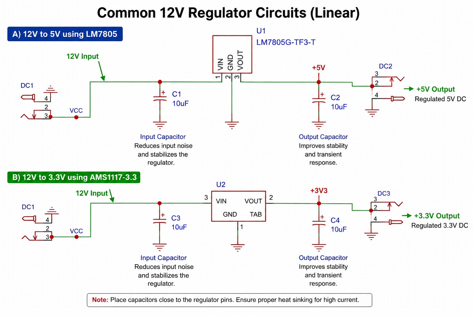
Figure 3. Circuit schematics for 12V to 5V LM7805 and 12V to 3.3V AMS1117-3.3 linear voltage regulators with filtering capacitors.
A fixed 7805-type regulator is a simple solution for a 12 V-to-5 V power supply rail. The circuit requires the regulator and the input and output capacitors recommended in the relevant datasheet, and it performs satisfactorily with moderate loads such as small logic sections, indicators, or auxiliary circuitry, provided the device's temperature remains within allowable limits.
You can construct a voltage regulator that converts 12 V to 3.3 V using a fixed LDO, for example, the AMS1117 is rated for up to 1 A, but at 12 V input the practical limit is closer to 100–250 mA depending on the available copper area, since a SOT-223 package has a thermal resistance of roughly 90 °C/W in free air and at best about 46 °C/W with a large copper pour. A larger voltage drop turns more power directly into heat: at 12 V input and 3.3 V output, even 300 mA already produces roughly 2.6 W of dissipation, which exceeds what a SOT-223 can safely dissipate (about 1.1 W in free air, and at best around 2.2 W with extensive copper), so the device would enter thermal shutdown—at this level, a buck converter is the right choice.
Also check the input rating before committing to this part: the original AMS1117 datasheet lists an absolute maximum input voltage of 15 V, and second-source versions differ in this limit, so a 12 V rail already runs close to it—always verify the specific supplier's datasheet. On an automotive 12 V system, load-dump and other transients rise far above this level, so a TVS diode or a pre-regulator stage must clamp the rail before it reaches the LDO. Since many variants of the AMS1117 depend on an appropriate output capacitor for stability, use a common value such as 10 µF as a starting point rather than a general rule. Note that the original AMS1117 datasheet calls for a 22 µF tantalum output capacitor, and that this family relies on the output capacitor's ESR for loop stability—directly substituting a low-ESR X7R ceramic can make the output oscillate, so check the specific manufacturer's capacitance and ESR requirements. Always confirm with the datasheet.
In each case, calculate the dissipation before choosing the package and PCB area. Linear solutions are usually practical only when the current is low, and the voltage is dropped from 12 . The precise safe current varies with ambient temperature, package thermal resistance, copper area, airflow, and the maximum allowable junction temperature. When the expected dissipation reaches several watts, a switching regulator is generally the right engineering choice.
Thermal Design for 12V Regulators
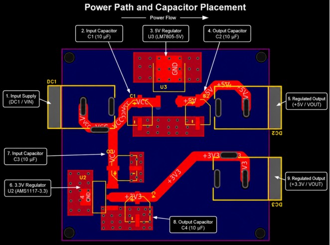
Figure 4. Two-layer PCB layout illustrating large top copper pour areas for thermal dissipation around 5V and 3.3V voltage regulators.
The thermal calculation is simple yet important; in a linear regulator reducing 12 V to 5 V at a current of 1 A results in about 7 W of heat, while reducing 12 V to 3.3 V at 0.5 A produces around 4.35 W. Since these figures are too high for a small SOT-223 regulator to dissipate safely on a normal PCB without taking aggressive thermal measures, a TO-220 device too might require a heatsink.
Table 1. Quick selection guide for 12 V linear regulators: voltage and current to power loss and recommended solution.
| Input → Output | Current | Power Loss | Recommended Solution |
|---|---|---|---|
| 12 V → 5 V | ≤ 100 mA | ≤ 0.7 W | SOT-223 / SOT-23 LDO, copper pour only, no heatsink |
| 12 V → 5 V | ~250 mA | ~1.75 W | TO-252 (DPAK) or TO-220 with generous copper pour |
| 12 V → 5 V | 500 mA | 3.5 W | TO-220 with heatsink — or switch to a buck converter |
| 12 V → 5 V | 1 A | 7 W | Use a buck converter (linear is impractical) |
| 12 V → 3.3 V | ≤ 100 mA | ≤ 0.87 W | AMS1117 (SOT-223) with copper pour |
| 12 V → 3.3 V | 500 mA | 4.35 W | TO-220 with heatsink at minimum; buck preferred |
Attaching copper to the regulator's heat-spreading tab reduces thermal resistance by spreading heat across the board. Thermal vias can transfer part of that heat to a copper area on the bottom layer. The larger and more continuous the usable copper area, the more effectively it can spread heat, but no single copper area can guarantee a particular temperature because the stack-up, airflow, copper weight, and enclosure conditions all affect it.
When the calculated power loss is in the range of several watts, don't use extra copper to replace the proper regulator topology. For 12 V conversion with higher current, a buck regulator is generally smaller, cooler, and more reliable than pushing a linear regulator near its thermal limit.
Voltage Regulator PCB Layout Best Practices
With linear regulators, the most important considerations on the printed circuit board are ensuring that the capacitors are properly connected, providing low-resistance power paths, having a clean ground return, and including sufficient copper to handle the heat; whereas with switching regulators there is another issue to take into account namely, minimizing the loop area at high frequency in order to control EMI.
Component Placement for Voltage Regulators
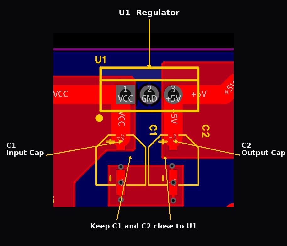
Figure 5. Detailed PCB layout view highlighting the close placement of input and output capacitors to the voltage regulator pins.
Position the input capacitor as close as possible to both VIN and the regulator ground connection and place the output capacitor directly next to VOUT and ground. When the package and routing allow it, a useful practical goal for a small regulator section is to keep the capacitors within a few millimeters of their respective pins.
Long traces increase resistance and inductance, causing voltage drop and making it harder to supply rapid local current changes. Make sure the route from the input connector to the regulator is sufficiently wide and carry the regulated output from the regulator to the load without unnecessary narrowing or detours. Position bulk capacitors, TVS devices, and reverse-polarity protection at the places where they are meant to protect or support the relevant node, not just because there is empty space left on the board. For general power-section placement rules, refer to our PCB Layout Process Guide 2026.
Ground Plane and Return Path Strategy
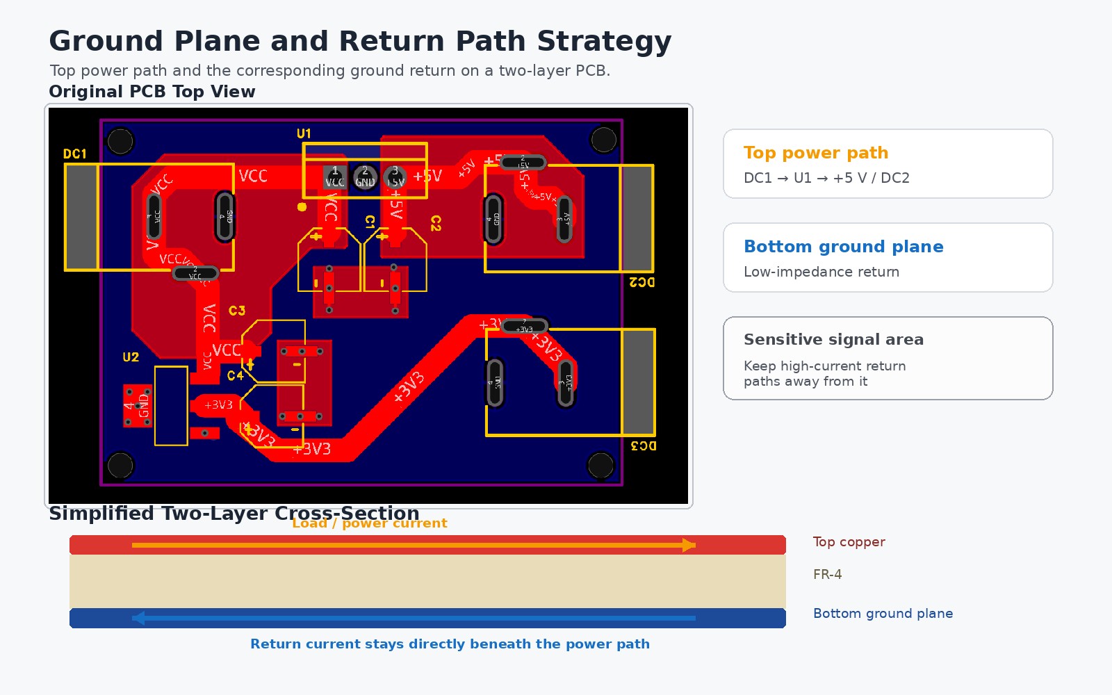
Figure 6. Diagram illustrating the top power path and corresponding bottom ground plane low-impedance return path in a two-layer PCB cross-section.
When the board layout permits, use a solid, continuous ground plane under the section containing the linear regulator; this gives the load current a low impedance return path and helps dissipate heat. Do not force the high-current return current through narrow signal-ground traces and only split the ground plane directly under the regulator if there is a clear reason at the system level.
With a linear regulator such as a 7805 or one from the AMS1117 series, no switching node causes the same high-frequency loop-area issue as in a buck converter; the ground plane mainly provides a clean reference, low resistance, and thermal spreading. In switching regulators, however, the return path around the high-di/dt loop must be much tighter because loop area directly affects ringing and EMI.
Thermal Management: Copper Pour and Thermal Vias
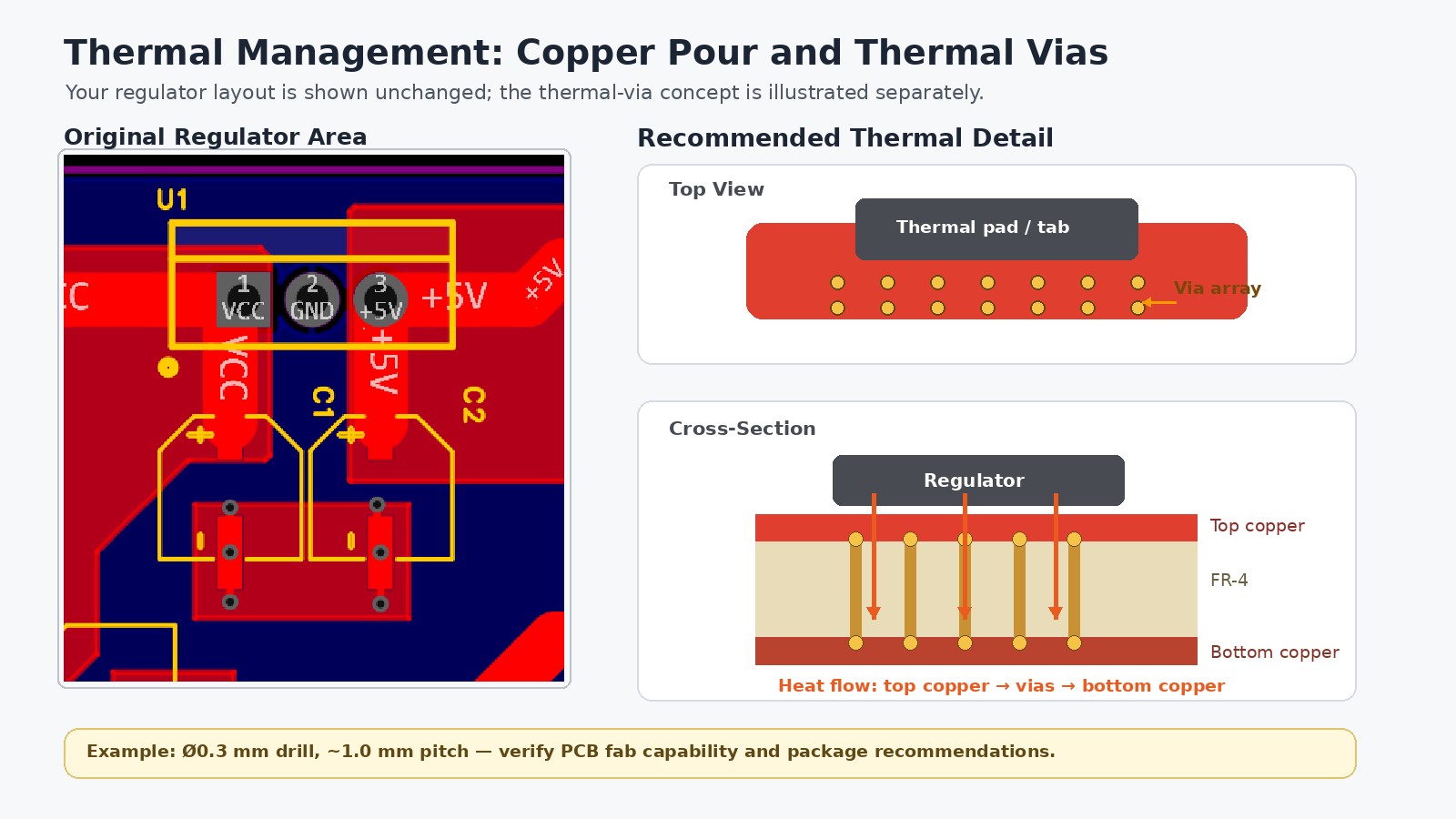
Figure 7. Diagram showing top view pad array and cross-sectional view of thermal vias transferring heat from top copper to bottom copper layer.
When using copper on the heat-spreading pin or exposed pad, use as much as the package permits, following the datasheet's recommended land pattern. If you need to share heat with the other side of the board, use plated thermal vias to connect the top copper to a copper area on the bottom. A typical starting point in PCB thermal design is a 0.3 mm finished drill with a pitch of about 1.0 mm. However, the exact via size must still correspond to the PCB manufacturer's capabilities, the soldering method, and the pad design. For reference, JLCPCB supports via holes down to 0.15 mm with 0.25 mm pads, so a 0.3 mm thermal drill sits comfortably within standard capability. One caveat matters more than size: when a via lands inside a solderable pad, molten solder can wick down the barrel during reflow and starve the joint, so vias placed in thermal pads should be plugged and capped—JLCPCB offers epoxy-filled, plated-over vias as the default process on 6-layer and above boards, which keeps the pads flat and solderable.
Copper pour and vias help reduce temperature rise, but they do not eliminate the need for a thermal calculation. Estimate the regulator's power loss, check the thermal data in the datasheet for junction-to-ambient or junction-to-case performance, account for the actual ambient temperature, and ensure the margin stays below the maximum junction temperature. If the board cannot dissipate the expected heat comfortably, use a heatsink, reduce the current, reduce the input voltage, or switch to a switching regulator. Board construction and copper weight are two further levers: a 4-layer board with solid internal copper planes spreads the same power loss far better than a 2-layer board, and moving from standard 1 oz to 2 oz outer copper noticeably lowers spreading resistance—both are standard selectable options when ordering from JLCPCB.
When selecting the width of traces that carry current, use an established sizing method such as IPC-2152 rather than choosing the width based on appearance. This principle also applies to thermal design: base dimensions on current and temperature requirements, not a general layout screenshot.
Key Components in a Voltage Regulator Circuit
An input capacitor
A small ceramic capacitor works well at high frequencies because of its low impedance. On the other hand, a larger electrolytic or polymer capacitor can supply the bulk energy needed when the supply cable is long or the load changes suddenly. Use the values recommended by the regulator manufacturer, and consider the voltage rating, temperature rating, and ESR.
The output capacitor
The output capacitor handles load transients and, in many LDOs, affects control-loop stability. It is not correct to think that 'the greater the capacitance the better'; some regulators do state a minimum value or specify an acceptable range of ESR.
Protection against reverse polarity
If the power supply might be connected backward, a series diode or MOSFET can protect the circuit board as part of a reverse-polarity stage. The method you select depends on the permitted voltage drop and current.
A TVS diode
A TVS diode is useful when the input is subject to transients, particularly on long cables, in automotive applications, or in industrial cabling. The diode's standoff and clamping ratings should correspond to the normal input voltage and the regulator's absolute maximum rating.
Protection diode across the regulator
In certain circuits, a diode connected from output to input protects the regulator against reverse current when the input voltage collapses, but the output capacitor is still charged. Whether it is necessary depends on the regulator and the circuit conditions.
LED indicator for power
An LED together with a series current-limiting resistor serves as a simple optional indicator for the regulated power supply. Select the resistor based on the rail voltage, the LED's forward voltage, and the desired LED current, and include that current in the regulator's load budget.
Common Voltage Regulator PCB Design Mistakes
Capacitors placed too far from the IC. The regulator sees extra trace inductance and resistance, which can worsen transients or even stability. Place the required input and output capacitors next to the regulator pins and use short ground connections.
Too little copper for heat spreading. A regulator may pass electrical testing for a few seconds, then overheat under continuous operation. Estimate power loss first and allocate copper or a heatsink before finalizing placement.
No thermal vias where they matter. A large bottom copper plane helps little if heat is trapped on the top layer. Where the package and assembly process allow it, use an appropriate via array to connect heat-spreading copper between layers.
Power routed through thin signal traces. Thin copper creates voltage drop and local heating. Size power tracks for the expected current and temperature rise, not for visual consistency with signal traces.
Ignoring the return path. Current always returns to its source. A poor ground route can introduce unwanted voltage differences across the board, so keep the power return broad, direct, and separated from sensitive signal paths where necessary.
FAQs about Voltage Regulator PCB
Q: What function does a voltage regulator have on a printed circuit board?
It supplies a regulated voltage to devices that cannot be connected directly to the unregulated power source and helps isolate the load from normal input variations, though the regulator must still be designed within its voltage, current, and thermal limits.
Q: What is the best way to decide between a linear regulator and a switching regulator?
Use a linear regulator when current is moderate, the voltage drop is small enough to manage thermally, and you need low noise or simplicity. Use a switching regulator when efficiency, battery life, or the need for high-current conversion makes the heating problem associated with a linear regulator impractical.
Q: What kind of capacitors do I need for a voltage regulator circuit?
The capacitors to be used as input and output should be the ones specified in the regulator's datasheet since their capacitance, the type of dielectric, the voltage rating, and in some cases the ESR have an effect on the transient response and stability; therefore, a general capacitor value should never be used in place of the manufacturer's recommendation.
Q: Can I use a voltage regulator PCB to change 12V to 5V?
Yes, a linear regulator of the 7805 type can be used with low-current loads, but the heat loss is approximately (12 - 5) times the load current. At higher currents, a buck converter is generally the best choice since it loses much less power.
Q: How much copper area do I need for thermal dissipation?
Since there is no universal answer, the required area depends on the package thermal resistance, copper thickness, number of layers, airflow, ambient temperature, via design, and maximum allowed junction temperature. Start with the thermal guidance in the regulator's datasheet, then verify the final design through calculations and temperature testing under worst-case load conditions.
Conclusion About Voltage Regulator PCB
Reliable voltage regulator PCB design involves considering the schematic, component selection, layout, and thermal path as a single system. Place the required capacitors close together, provide direct copper routes for power and ground currents, and calculate heat before concluding that a linear regulator can handle a 12 V conversion. If dissipation is too high, it is usually better to switch to a switching regulator than to increase the copper around an already overloaded linear device.
JLCPCB layout engineers can turn the design into a finished product once you've checked the regulator datasheet, PCB design rules, and thermal assumptions.
Keep Learning
Bypass Capacitor Placement in PCB Layout: Best Practices
Quick answer:Bypass Capacitor Place each bypass capacitor as close as possible to the IC's power and ground pins, connect it with short, wide traces, and drop dedicated vias to the power and ground planes right at the capacitor pads — never between the IC and the capacitor. Every millimeter of trace adds roughly 1 nH of parasitic inductance, which raises the loop impedance (Z = 2πfL) and defeats the capacitor at high frequencies. The smaller the capacitor value, the closer it must sit to the pin. Intr......
Track Width v/s Current Capacity: PCB Layout Tips for Power Routing
Key Takeaways Trace width and copper thickness set the current limit. Standard 1 oz (35 µm) copper suits most designs; step up to 2–3 oz for power-hungry boards. Size traces against IPC-2221/IPC-2152 for a safe temperature rise. Internal layers carry less current than external ones. Buried traces dissipate heat poorly, so derate them or move high-current paths to outer layers. Vias are a bottleneck—each carries only about 500 mA. When routing power across layers, stitch multiple vias in parallel rathe......
Circuit Board Ground Plane and Power Plane Guide 2026
Key Takeaways Continuous copper first: A solid circuit board ground plane creates a low-impedance return path, reduces noise, and is usually safer than split planes, even on mixed-signal boards. Think in current loops: Every signal needs a return path directly beneath it. Never route high-speed traces across plane gaps, slots, or cutouts. Plan the stack-up early: Choose the layer arrangement before routing critical signals, and keep power and ground planes close together to lower distribution inductan......
Guide to Ground Bounce in PCB - Causes, Effects & Prevention
Key Takeaways Ground bounce is a voltage spike between an IC's die ground and the PCB ground. It happens when current changes fast through parasitic inductance (V = L x di/dt). Many outputs switching at once, called SSO, make it much worse. It can cause logic errors, false resets, and ringing on signals. You measure it with a quiet-low sense line on a scope. Good decoupling, short ground loops, and slower slew rates fix most of it. Introduction A board passes every test on the bench. Then, in the fiel......
Voltage Regulator PCB: Practical Design Guide
Key Takeaways A voltage regulator PCB doesn't just convert one voltage into another; it must also provide a stable output while handling heat, load changes, and noise in the circuit. The layout is as important as the regulator IC; keep the input and output capacitors near the pins, use short power connections, and ensure a direct, low-impedance ground return. Linear regulators are simple and quiet, but they lose voltage difference as heat; switching regulators are the better option when the voltage dr......
LDO vs Switching Regulator: Comparison & PCB Layout
Key Takeaways Calculate LDO dissipation first: Always calculate LDO power dissipation at maximum input voltage and load before comparing packages or prices. Condition-dependent specs: Treat dropout, PSRR, noise, ripple, efficiency, and transient response as condition-dependent, not fixed values. Layout matters for both: A buck converter's high-di/dt input loop and high-dv/dt switch node create different coupling mechanisms. Both need deliberate PCB placement. Output capacitor selection: The output cap......