Boost Converter PCB: A Practical Layout Guide for Engineers
25 min
- Key Takeaways
- Introduction
- Boost Converter PCB Diagram: Where the Current Actually Flows
- Boost Converter PCB Layout: Five Rules for Efficiency and EMI
- Trace Width, Copper Weight, and Via Current Capacity
- Stackup Choice and a Boost Converter PCB Example
- Common Boost Converter PCB Layout Mistakes
- Boost Converter PCB Layout Checklist
- FAQs About Boost Converter PCB
- Conclusion About Boost Converter PCB
Key Takeaways
- In a boost converter, the pulsed high-di/dt loop is switch, diode, and output capacitor, not the input loop. Place those three parts first.
- Keep the switch node to the smallest copper shape that carries the current. Never pour it for cooling.
- Run one continuous ground plane under the power stage, with no splits.
- Size copper and vias from RMS current and duty cycle, not from average output current.
- A 10-minute checklist review before release prevents most re-spins.

Introduction
The board simulated cleanly. Then the first prototype runs hot, the output ripple doubles at full load, or radiated emissions fail somewhere between 30 and 100 MHz. The schematic is rarely the cause. The boost converter PCB is. A boost converter steps a lower DC input up to a higher regulated output, and the layout decides whether it does that quietly or noisily.
Most boost converter design effort goes into the inductor, the compensation, and the component ratings. Copper placement can undo all of it. The switching regulator layout rules are the same ones that decide whether a boost runs cool; what changes is which loop carries the pulsed current. Two boards with identical schematics can differ by several degrees of heating and a full EMC margin, purely because of where the diode sits.
This guide covers the current-path diagram that drives every placement decision, five layout rules, copper and via sizing, stackup, a complete schematic with real PCB screenshots of a worked 5 V example, common mistakes, and a checklist you can use on your own board.
Boost Converter PCB Diagram: Where the Current Actually Flows
Before placing a single part, mark where the current flows. A schematic shows connections, but not which wires carry steady current and which carry sharp, pulsed edges. That difference decides every placement choice that follows. Figure 1 gives the complete schematic for the example used throughout this article, then overlays the two current paths on top of it.
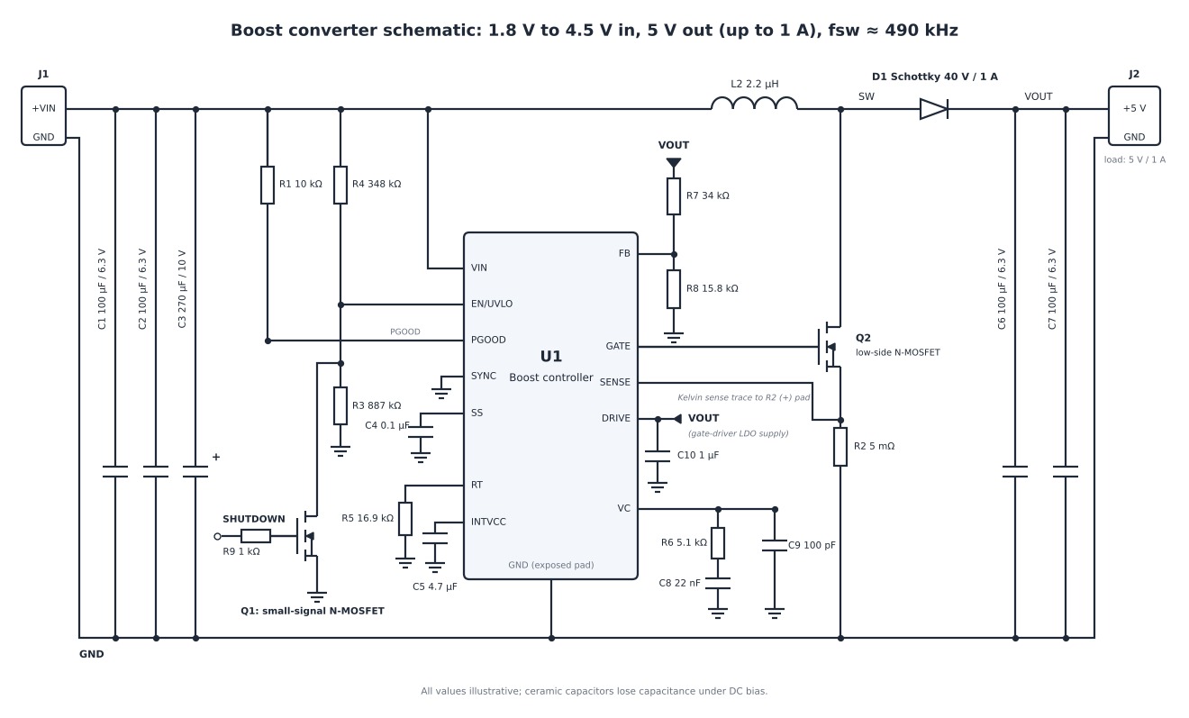
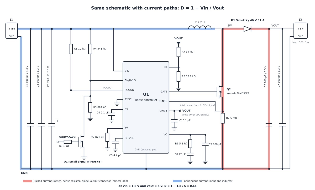
Figure 1. Complete schematic of the 5 V / 1 A example, 1.8 V to 4.5 V input (top), and the same schematic with the pulsed switch, sense-resistor and diode path in red and the continuous input and inductor path in blue (bottom).
The same values are used for the board shown later, so you can rebuild it as drawn. Q1 and R9 form an optional shutdown input and R1 pulls up the power-good pin; neither touches the power path. One detail to add if the shutdown input is optional: a 100 kΩ gate-to-source resistor on Q1, so its gate cannot float when nothing drives the input.
| Part | Value |
|---|---|
| Input / output | 1.8 V to 4.5 V in, 5 V out at up to 1 A (5 W) |
| Switching frequency | About 490 kHz (RT = 16.9 kΩ) |
| Inductor L2 | 2.2 µH, shielded, saturation current ≥ 4 A as built (5 A recommended with the 11 mΩ sense resistor) |
| Input capacitors C1–C3 | 2 × 100 µF / 6.3 V + 270 µF / 10 V bulk |
| Output capacitors C6, C7 | 2 × 100 µF / 6.3 V |
| Diode D1 | D1 (VD1 on the board), 40 V / 1 A Schottky (2 A recommended) |
| Low-side MOSFET Q2 | 60 V logic-level, about 12 mΩ RDS(on) (see the cold-start note) |
| Feedback divider R7 / R8 | 34 kΩ / 15.8 kΩ (1.6 V reference, about 5 V out) |
| UVLO divider R4 / R3 | 348 kΩ / 887 kΩ (turn-off ~1.7 V, start ~2.4 V) |
| Soft-start C4 / INTVCC C5 | 0.1 µF / 4.7 µF |
| DRIVE bypass C10 | 1 µF at the DRIVE pin (missing from the rev A layout; add it in rev B) |
| Current-sense resistor R2 | 5 mΩ as built (limit ~10 A); 11 mΩ recommended (limit ~4.5 A) |
| Compensation R6 / C8 / C9 | 5.1 kΩ / 22 nF / 100 pF |
The UVLO divider and Q2 are the two places where rev A falls short of its 1.8 V label. The divider turns off at 1.22 V × (1 + 348/887) ≈ 1.70 V, but the EN/UVLO pin pulls about 2 µA through the 348 kΩ upper resistor between 0.7 V and 1.22 V, so the board starts at about 2.4 V. The 1.8 V numbers in this article are the operating worst case after startup, not the cold-start point. Q2 has a similar low-voltage caveat. At the 2.4 V start point, the VIN LDO gives the gate driver only about 2.0–2.2 V; if you lower the divider for a true 1.8 V start, that falls to about 1.4–1.6 V. A 60 V logic-level FET is usually specified at 4.5 V gate drive, so check RDS(on) at the actual gate voltage and use a low-threshold part if you need a true 1.8 V cold start.
Two connections in Figure 1 are easy to misread, so they are called out here. The LT3759 datasheet is clear that DRIVE is not a gate output. It is the supply pin of the internal LDO that generates INTVCC for the gate driver, and the datasheet allows it to be tied to VIN or to a quasi-regulated supply such as a converter output. Here it is tied to the 5 V output, which makes INTVCC about 4.75 V once the converter is running. C10 is the 1 µF bypass at the DRIVE pin, as the datasheet requires, but the rev A layout left it out; add it next to pin 10 before you copy the board. The GATE pin is the separate gate-drive output to Q2.
SENSE is drawn as a Kelvin connection: a dedicated trace to the positive pad of the sense resistor R2, not to the Q2 source node. Rule 5 explains how to route it.
Two Current Loops, Two Very Different Jobs
A boost converter is not a buck converter turned around, and the layout rules do not transfer one-to-one. On the input side, the inductor sits in series with the source, so current flows continuously and only ramps up and down by the ripple amount. That side is quiet.
On the output side, the diode conducts only while the switch is off. The output capacitor and the load therefore see current delivered in pulses at the switching frequency. Every cycle, that current commutates abruptly between the switch and the diode.
The consequence is simple. The critical loop is switch, sense resistor, diode, output capacitor, and the ground return back to the switch. Any inductance in that loop turns a sharp current edge into a voltage spike and a radiated field. It is the EMI source and the main heating path at the same time.
Turning Boost Converter Design Numbers into Layout Rules
Four numbers from the example, worked at its worst case of 1.8 V in and 1 A out, translate directly into copper decisions:
- Duty cycle: D = 1 − Vin / Vout = 0.64 (only 0.10 at 4.5 V in)
- Average inductor current: IL = Pout / (η × Vin) = 3.1 A, assuming 90% efficiency
- Switch current: average IL × D = 2.0 A, RMS IL × √D ≈ 2.5 A
- Inductor ripple: ΔIL = Vin × D / (L × fsw) = 1.1 A (2.2 µH, 490 kHz), so IL peaks near 3.6 A
Duty cycle sets how conduction loss splits between the switch and the diode. The switch RMS value, never IL itself, sizes the copper around it. Ripple sets the ripple current in the output capacitor and the core loss in the inductor. These are the same values a boost converter equation sheet or an online boost converter calculator gives you, so reuse your own numbers. For the full boost converter design procedure, follow your controller's datasheet or a design calculator; this article only connects those results to the board. The table below works the same numbers at both ends of the 1.8 V to 4.5 V input range.
| Quantity | Formula | Vin = 1.8 V (worst case) | Vin = 4.5 V |
|---|---|---|---|
| Duty cycle D | 1 − Vin / Vout | 0.64 | 0.10 |
| Average inductor current IL | Pout / (η × Vin), η = 0.9 | 3.1 A | 1.2 A |
| Inductor ripple ΔIL | Vin × D / (L × fsw) | 1.1 A | 0.4 A |
| Inductor peak current | IL + ΔIL / 2 | 3.6 A | 1.4 A |
| Switch RMS current | IL × √D | 2.5 A | 0.4 A |
| Diode RMS current (average is 1 A) | IL × √(1 − D) | 1.9 A | 1.2 A |
| Output capacitor ripple current (RMS) | Iout × √(D / (1 − D)) | 1.3 A | 0.3 A |
| Capacitive output ripple | Iout × D / (fsw × C), C = 100 µF effective | 13 mV | 2 mV |
The worst case is the lowest input, not the highest. At 1.8 V the inductor peaks near 3.6 A, so specify a saturation current above the current limit, 5 A or more. R2 is the next thing to look at. At 5 mΩ, the controller's 50 mV current-limit threshold (46–54 mV over temperature) puts the limit at about 10 A, nearly three times the 3.6 A peak and far above the inductor's saturation rating. That keeps it from limiting at start-up but protects poorly against a short. The 40 mV in the datasheet's sizing equation is a design target, 20% below the 50 mV limit, not the limit itself. Sized from that target, R2 should be about 11 mΩ, which limits near 4.5 A, just under the 5 A saturation rating.
Losses come next. At 1.8 V in, the diode burns the most, roughly 0.5 W at about 0.5 V forward drop. The inductor adds about 0.2 W, assuming 20 mΩ of winding resistance, and the switch and R2 together add about 0.1 W. That totals about 0.8 W, or roughly 86% efficiency, so the 90% figure above is a little optimistic. The diode also runs right at its 1 A average rating, with an RMS current of 1.9 A, so it has no margin; specify a 2 A part in the same footprint. Either way, its copper matters in Rule 4. Finally, C6 and C7 are 6.3 V ceramics running at 5 V. That is only 1.26× the rail, and DC bias can halve their capacitance, so the table assumes only 100 µF effective. For production, specify 10 V or 16 V parts for C6 and C7 and 10 V for the input ceramics C1 and C2; at 5 V and 4.5 V, the higher-rated parts keep far more of their capacitance.
Boost Converter PCB Layout: Five Rules for Efficiency and EMI
These five rules explain most of the difference between a board that runs cool and passes EMC and one that runs hot and fails emissions. In order: shrink the pulsed loop, minimize the switch node, keep the ground plane whole, place the magnetics and diode deliberately, and protect the feedback path. They apply whether the design uses a controller IC with an external MOSFET, an integrated switcher, or a discrete gate driver. The thermal advice differs between those cases, as Rule 2 explains.
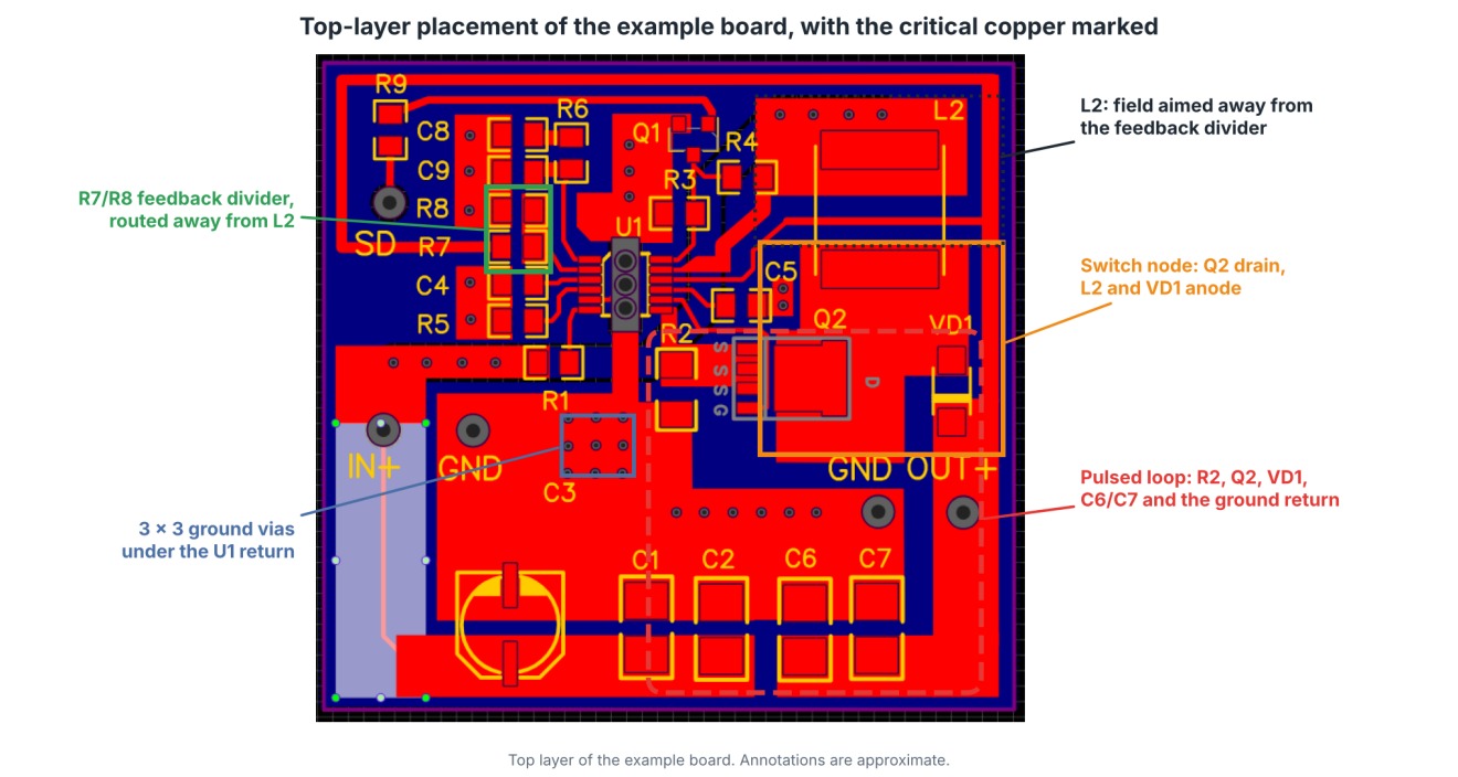
Figure 2. Top view of the rev A example board with the critical copper marked. The red outline is the pulsed loop, which is longer than it should be; the orange box is the switch node, and the feedback divider sits on the far side of U1 from L2. C10 is missing from this layout; add it at the DRIVE pin in rev B.
Rule 1 – Keep the Switch-Diode-Output Loop Tiny
Boost converter PCB layout starts with one compact cluster: the switch, its sense resistor, the diode, the output capacitor, and the ground return between them. Place them so the loop through all of them is as short and wide as possible, with the least stray inductance between any two of them. Every additional millimeter of separation adds loop inductance, and that inductance feeds directly into the switch-node voltage spike and the radiated field strength.
TI's five-step boost converter layout application note (SLVA773) reaches the same conclusion, treating output capacitor placement as the most important step. It also notes that a snubber is not needed for normal operation and is added only when EMI demands it. In practice, a lower loop inductance means a lower turn-off spike, which reduces the ringing a snubber would have to damp.
Keep the loop on one layer where possible. Never stub it or neck it down. Where a via is unavoidable, use several in parallel so the path still behaves as a low-inductance connection, and let the return current flow in the ground plane directly below the loop (Rule 3).
The input capacitor is less critical, but not irrelevant. The inductor keeps the input current continuous, so CIN sits outside the pulsed loop. Land its ground terminal close to the controller's power-ground pin and give it solid copper, but do not shorten the input-to-inductor distance at the expense of the output loop. Figure 2 shows the intent: the red loop should get the tightest geometry on the board, and everything else should be arranged around it. On this rev A board the loop is still longer than it should be; the example walkthrough shows where it went wrong.
Rule 2 – Treat the Switch Node as a Radiating Antenna
The switch node is the dv/dt node. Keep its copper to the smallest shape that carries the current. No pour "for cooling," no test point, no via, and no unrelated trace underneath or alongside. Keep it away from board edges, connectors, and the feedback network.
A hot switch tempts new engineers to add copper here, but the right fix depends on the device:
- Integrated switcher with a grounded pad. If the datasheet says the exposed pad is ground, heat leaves through the pad and an array of thermal vias into the ground plane on the bottom or an inner layer.
- Discrete low-side MOSFET. The exposed pad is usually the drain, which is the switch node. Vias from that pad to ground would short the node. Pad copper is a trade-off, small for EMI and large for heat, so remove heat by cutting loss (lower RDS(on), better gate drive, lower switching frequency) and by letting the input, output, and ground copper act as the heatsink. A source-down package, whose pad is source and ground, is an option when thermals dominate. Confirm what the pad connects to in the datasheet first.
Never enlarge the switch node on the assumption that it cools the part. If ringing is still excessive, add an RC snubber in one of two places: across the MOSFET, returning to the source and power ground, or across the diode, hugging its two terminals. Either way, the snubber's own loop must stay as small as possible.
Rule 3 – Use One Continuous Ground Plane Under the Power Stage
Return current follows the path of least inductance, which is directly under the signal path. Under the pulsed loop, a solid ground plane gives that current a tight mirror image to follow, and the two opposing currents cancel much of each other's field.
Do not split the ground plane under the power stage. The classic "split power and analog ground" habit backfires here: it lengthens the return path and turns the gap into a slot radiator. If the feedback network needs a quiet ground, allow a single-point tie between the analog ground and the power ground, placed at the controller, and keep the plane itself whole.
Add stitching vias around the power stage so the ground layers behave as one low-impedance surface. Do not use thermal reliefs on high-current pads. Reliefs are a soldering convenience, and on a power pad they add inductance and resistance exactly where the pulsed current returns. Connect those pads solidly to the plane.
Rule 4 – Place the Inductor and Diode for Heat and Field
The inductor is the largest heat source and the largest magnetic field on the board. Orient it so its field is not aimed at the feedback divider or the sense lines, and keep as much clearance from sensitive analog parts as the layout allows. A shielded inductor helps, but it does not replace distance.
Give the diode its copper on the output side. The heat-spreading pour belongs on the cathode (output) terminal, never on the switch-node terminal, which would enlarge the dv/dt node and undo Rule 2. The two copper areas must not merge.
Check the output capacitor for ripple-current self-heating. At D = 0.64 the ripple current in COUT is about 1.3 A RMS in the example, higher than the 1 A load current, and ceramic banks share it better than a single electrolytic does. Keep electrolytics away from the diode, since heat shortens their life.
Settle all of this before routing starts. Placement is the cheapest fix available, and moving a diode on a finished board costs far more than moving it on an empty one.
Rule 5 – Keep the Feedback Divider and Sense Lines Quiet
Route the feedback trace short and direct from the divider to the controller, with ground copper beside it. Never run it under or beside the inductor or the switch node. Put the divider near the controller, not near the output connector, so the long, noisy stretch is not the high-impedance one.
For current sense, use a Kelvin connection. The controller's SENSE pin gets its own trace to the positive pad of the sense resistor R2, not to the MOSFET source node, and the controller ground lands close to the ground terminal of R2, so the two sense conductors form a pair. Route them together, outside the pulsed loop. The resistor itself sits in the pulsed loop, so place it tight against the MOSFET source and let only the sense traces leave the loop.
The failure mode to recognize is a noisy feedback node. It produces jitter and output ripple that no capacitor change will fix. Note that control-loop instability, for example at duty cycles above 50%, is a compensation problem rather than a layout one. Do not chase it with copper changes.
Trace Width, Copper Weight, and Via Current Capacity
Size power-path copper from RMS current and the allowable temperature rise (IPC-2221-style curves), not from the average output current. The worked example shows why. At 1.8 V in and 5 V out at 1 A, D is about 0.64, IL is about 3.1 A, and the switch RMS current is about 2.5 A, even though the average switch current is only 2 A. A boost converter design that sizes copper from the 1 A output would be undersized on the inductor side by a factor of three.
For the pulsed path, 1.5 mm (60 mil) of 1 oz copper holds a 10 °C rise at the 2.5 A switch RMS current; 2 mm (80 mil) is good for about 4 A and leaves margin for peak current and pad neck-downs. Above about 5 A, move to 2 oz copper or parallel layers. For vias, a rule of thumb is that one 0.3 mm (12 mil) via carries about 1 A at a 10 °C rise, so use arrays of 4 to 8 where a net changes layers.
| Net | RMS Current | Trace Width | Copper Weight | Vias |
|---|---|---|---|---|
| Input to inductor | ~3.1 A | 2 mm (80 mil) | 1 oz | 4 if layer change |
| MOSFET drain / switch node | ~2.5 A | 1.5 mm (60 mil), minimal pad | 1 oz | None (top layer only) |
| Diode and cathode to COUT | ~1.9 A | 1.5 mm (60 mil) | 1 oz | None (top layer only) |
| Output to load | 1 A DC | 1 mm (40 mil) | 1 oz | 2 |
| Power ground return | ~2.5 A | Bottom-layer pour | 1 oz | 6 per cluster |
| Feedback | under 1 mA | 0.2 mm (8 mil) | 1 oz | 0 to 1 |
Watch for neck-downs at pads, where a wide trace squeezes into a narrow footprint and becomes the hottest spot on the net. Avoid 90-degree corners on high-di/dt nets; use two 45-degree bends or an arc.
Stackup Choice and a Boost Converter PCB Example
Stackup is the cheapest EMI decision available. It costs nothing at the layout stage, and it can save a re-spin. Below is a decision rule for two versus four layers, followed by the worked example board.
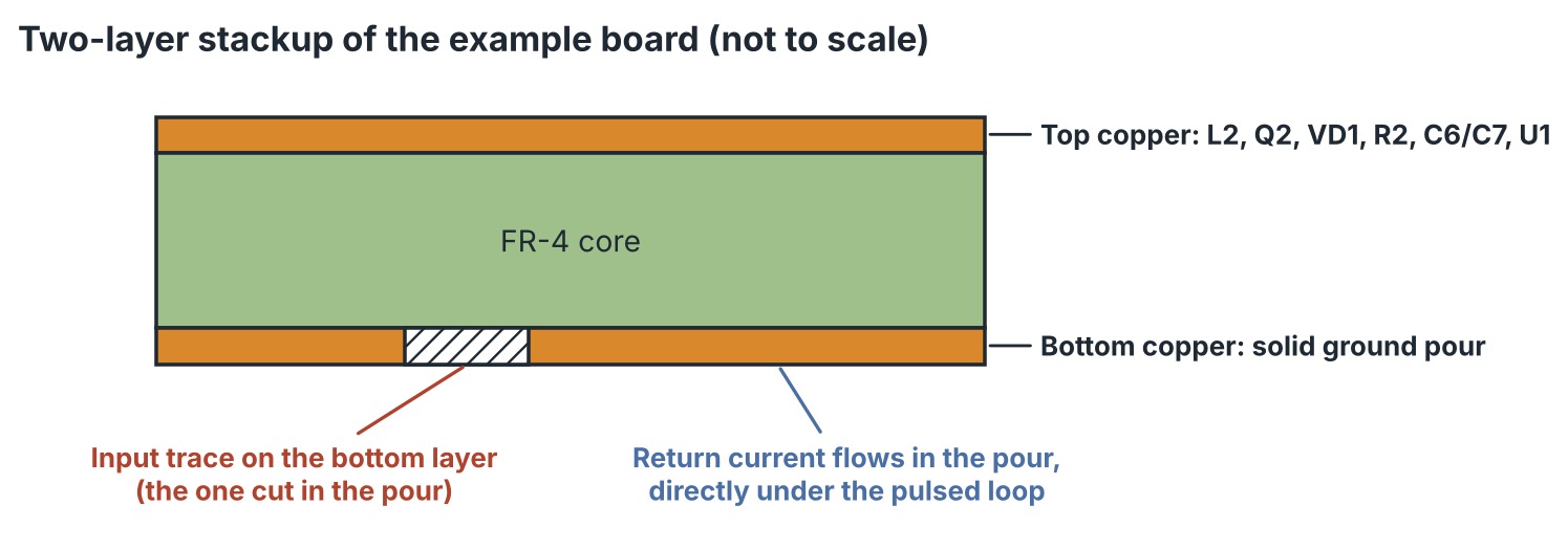
Figure 3. Two-layer stackup of the example board: the power stage and controller on top, and a solid ground pour on the bottom with the input trace as the one cut in it.
Two Layers or Four?
Base the choice on switching frequency, edge speed, current level, and EMC limits rather than a single wattage cutoff. A two-layer board with a solid bottom ground pour and a disciplined loop works for low-frequency, low-current designs with relaxed emissions limits. Four layers become the safer choice when the current is high, the edges are fast, the switching frequency is high, or the EMC margin is tight, because a full ground plane sits directly under the loop at a small spacing.
The cost trade-off is real: four layers cost more per board, though usually less than a failed EMC test and a re-spin. Agree on stackup and copper weight with your fabricator early.
Boost Converter PCB Example: 5 V Output at 1 A
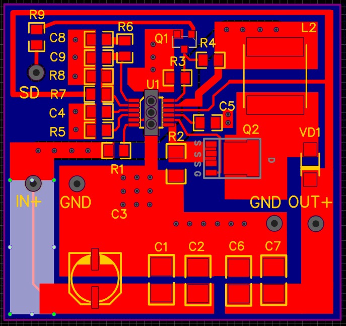
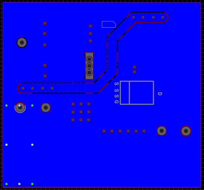
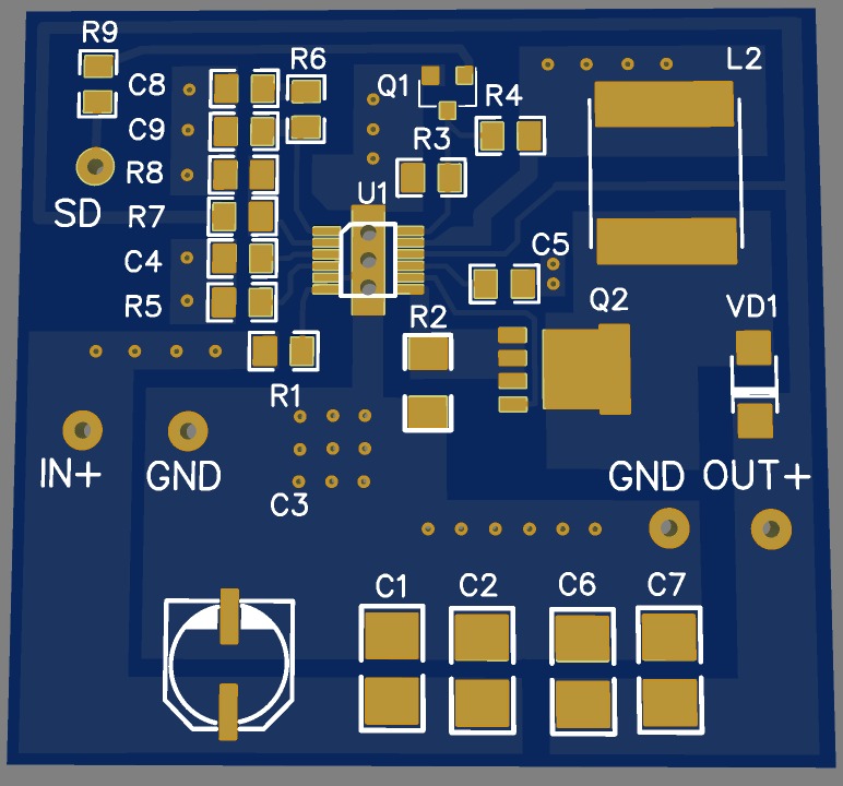
Figure 4. Boost converter PCB example (rev A), 1.8 V to 4.5 V design, 5 V / 1 A out on two layers: (a) top layer, (b) bottom layer with the ground pour and the input trace, (c) 3D view. Rev A as built starts at about 2.4 V; see the UVLO note.
The example board measures 45 × 45 mm (about 1.77 × 1.77 in) on two layers. The top layer holds the power stage and the controller. The bottom layer is a ground pour with one deliberate exception, a wide trace that carries the input current from the connector to L2. Walk through it in signal order, following the six stops below.
- Input connector and CIN. IN+ and GND come in at the left edge. The 270 µF bulk capacitor C3 and the ceramics C1 and C2 sit just behind them, and the input current then leaves on the bottom-layer trace, through four vias at each end.
- Inductor. L2 sits in the top-right corner, as far from the feedback divider as this board allows.
- Switch and diode. Q2 sits beside U1 with R2 right at its source pins. D1 (labeled VD1 on the board) is on the right edge, one pad away from the drain copper.
- Output capacitor. C6 and C7 sit along the bottom edge, not against the diode. The cathode copper runs down the right edge to reach them, so the pulsed loop is longer than I would like.
- Controller. The exposed pad of U1 ties through a short strip into a 3 × 3 via array that drops into the bottom ground pour.
- Divider and load. R7 and R8 sit on the left of U1, with the feedback trace kept away from L2 and the switch node. OUT+ and its ground are on the right edge.
These numbers come from the schematic and the calculations above, not from bench measurements, so treat the efficiency and ripple figures as estimates.
This is rev A, and it is a before board, not a template. Four changes define rev B. First, add the 1 µF DRIVE bypass C10 at pin 10; the layout left it out. Second, shrink the switch-node copper under Q2 and out to D1, since the MOSFET drain tab needs some copper but not this much. Third, move C6 and C7 against the diode cathode instead of down the board. Fourth, re-route the input trace on the top layer so the bottom ground pour stays whole. Shrinking the switch node and moving the output capacitors together shorten the loop and lower the turn-off spike; the input re-route removes the slot under the pulsed loop. The UVLO and Q2 caveats noted above are the other reasons rev A cannot cold-start at 1.8 V. I have not measured any of it, so treat these as the first places to look on a respin.
Common Boost Converter PCB Layout Mistakes
Four failures account for most of the boost converter PCB problems that reach a bench. Each has a recognizable symptom, a root cause, and a short fix.
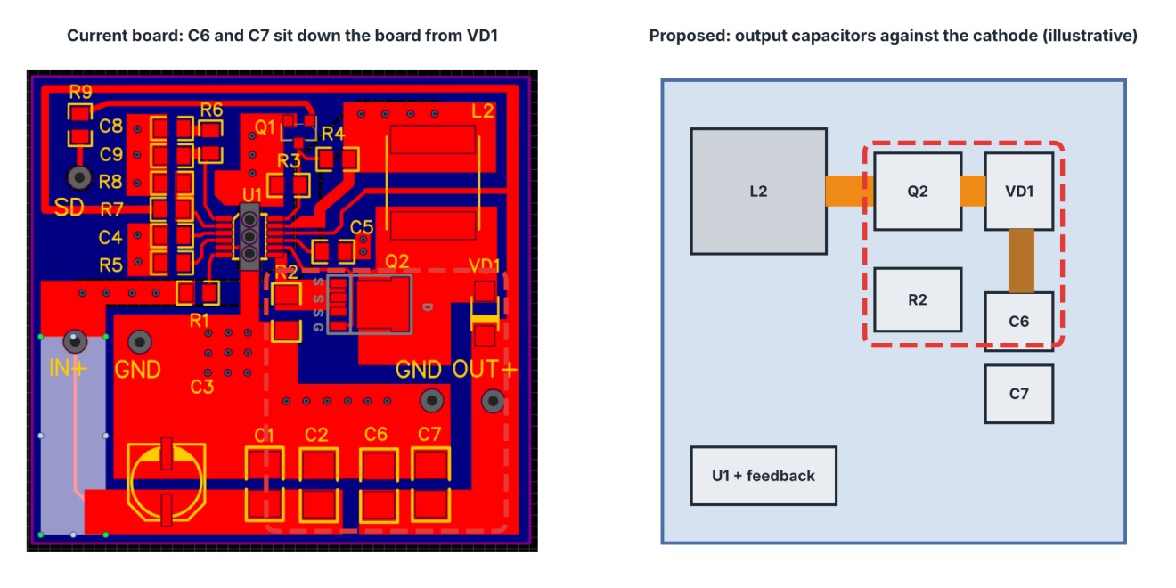
Figure 5. Left: rev A, where C6 and C7 sit down the board from D1 and the pulsed loop is large. Right: a proposed placement with the output capacitors against the diode cathode (illustrative).
Treating the boost like a buck. The symptom is a large voltage spike and warm diode even though the input capacitor sits perfectly. The cause is optimizing the input loop while the output loop stays huge. Fix it by moving the diode and COUT together first.
Pouring copper on the switch node for thermal reasons. The symptom is poor EMC with little thermal benefit. For a discrete low-side MOSFET the pad is the switch node, so the pour only enlarges the antenna; heat must come from lower loss, a better package, and the input, output, and ground copper. For an integrated switcher with a grounded pad, the pad gets a via array into the ground plane. Assuming both devices behave the same is the actual mistake.
Splitting ground between power and control. The symptom is ringing and radiated noise that changes when you probe the board. The cause is a lengthened return path and a slot radiator. Fix it with one plane and a single-point tie for the quiet ground.
Routing feedback under the inductor or across the pulsed loop. The symptom is jitter and output ripple that survives every capacitor swap. The cause is magnetic and capacitive pickup. Move the trace to the far side of the controller with ground beside it.
Boost Converter PCB Layout Checklist
Use this boost converter PCB layout checklist as a final pass before release; every row can be verified by eye in a layout review.
| Check Item | What Good Looks Like | Why It Matters |
|---|---|---|
| Pulsed loop area | Switch, diode, and COUT touching, loop on one layer | Sets spike height and radiated field |
| Switch node area | Smallest shape that carries the current, no vias or test points | Limits dv/dt radiation |
| Ground continuity | Unbroken plane under the power stage, no slots | Keeps the return path short |
| Input capacitor ground return | Close to the controller power-ground pin on solid copper | Less critical than the output loop, but still matters |
| Inductor orientation and clearance | Field aimed away from feedback and sense lines | Reduces pickup and ripple |
| Output capacitor | Ripple-current rating checked, placed against the diode | Prevents self-heating and keeps the loop small |
| Feedback and sense routing | Short, grounded, clear of inductor and pulsed loop | Prevents jitter and ripple |
| Copper and via sizing | Sized from RMS current, via arrays of 4 to 8 | Avoids hot spots and voltage drop |
FAQs About Boost Converter PCB
What is the most important rule when laying out a boost converter PCB?
Keep the switch, diode, and output capacitor loop as small as possible. That loop carries the pulsed current, so its inductance sets the voltage spike, the radiated EMI, and a large share of the heating.
Can I use a two-layer board for a boost converter?
Yes, for low-frequency, low-current designs with relaxed emissions limits, provided the bottom layer is a solid ground pour and the pulsed loop is tight. Go to four layers when current, frequency, or EMC margin tighten, because a full ground plane sits directly under the loop.
Why does my boost converter run hot or show high ripple at full load?
Check the output loop first. A long diode-to-capacitor path adds spikes and loss, and an undersized RMS rating on the inductor, diode, or capacitor adds heat. Your boost converter design calculation tells you the RMS values to compare against, so measure the board against those numbers.
Where should the output capacitor go in a boost converter layout?
Directly against the diode cathode, with its ground terminal on the shortest path back to the switch source or controller power-ground pin. Place the bulk capacitor farther away, near the output connector.
Conclusion About Boost Converter PCB
Three ideas carry most of a good Boost Converter PCB. First, the pulsed loop is on the output side: the switch, diode, and output capacitor must sit as one tight cluster. Second, keep one continuous ground with a minimal switch node, and resist the urge to pour copper there. Third, size copper and vias from RMS current, not average output current.
These are layout decisions made once and paid for forever. They cost nothing to get right on an empty board and a great deal to fix on a built one. Run the checklist above before release, and the rest of the debugging stage tends to be short.
If you would like a second set of eyes on your power stage, the team at JLCPCB's PCB layout services can review the loop, ground, and stackup while changes are still easy to make.
Keep Learning
Boost Converter PCB: A Practical Layout Guide for Engineers
Key Takeaways In a boost converter, the pulsed high-di/dt loop is switch, diode, and output capacitor, not the input loop. Place those three parts first. Keep the switch node to the smallest copper shape that carries the current. Never pour it for cooling. Run one continuous ground plane under the power stage, with no splits. Size copper and vias from RMS current and duty cycle, not from average output current. A 10-minute checklist review before release prevents most re-spins. Introduction The board ......
The Engineer's Guide to High Current PCB Design 2026
Key Takeaways System-Level Thinking: High current PCB design is about the entire power path — traces, vias, copper planes, connectors, component pads, and return paths working together. One weak link can cause voltage drop, overheating, or long-term failure. Common Failure Points: Undersized traces, insufficient via arrays, broken ground plane continuity, over-reliance on IPC tables without derating, and overlooked connector contact resistance are the five most frequent causes of high-current board fa......
Bypass Capacitor Placement in PCB Layout: Best Practices
Quick answer:Bypass Capacitor Place each bypass capacitor as close as possible to the IC's power and ground pins, connect it with short, wide traces, and drop dedicated vias to the power and ground planes right at the capacitor pads — never between the IC and the capacitor. Every millimeter of trace adds roughly 1 nH of parasitic inductance, which raises the loop impedance (Z = 2πfL) and defeats the capacitor at high frequencies. The smaller the capacitor value, the closer it must sit to the pin. Intr......
Track Width v/s Current Capacity: PCB Layout Tips for Power Routing
Key Takeaways Trace width and copper thickness set the current limit. Standard 1 oz (35 µm) copper suits most designs; step up to 2–3 oz for power-hungry boards. Size traces against IPC-2221/IPC-2152 for a safe temperature rise. Internal layers carry less current than external ones. Buried traces dissipate heat poorly, so derate them or move high-current paths to outer layers. Vias are a bottleneck—each carries only about 500 mA. When routing power across layers, stitch multiple vias in parallel rathe......
Circuit Board Ground Plane and Power Plane Guide 2026
Key Takeaways Continuous copper first: A solid circuit board ground plane creates a low-impedance return path, reduces noise, and is usually safer than split planes, even on mixed-signal boards. Think in current loops: Every signal needs a return path directly beneath it. Never route high-speed traces across plane gaps, slots, or cutouts. Plan the stack-up early: Choose the layer arrangement before routing critical signals, and keep power and ground planes close together to lower distribution inductan......
Guide to Ground Bounce in PCB - Causes, Effects & Prevention
Key Takeaways Ground bounce is a voltage spike between an IC's die ground and the PCB ground. It happens when current changes fast through parasitic inductance (V = L x di/dt). Many outputs switching at once, called SSO, make it much worse. It can cause logic errors, false resets, and ringing on signals. You measure it with a quiet-low sense line on a scope. Good decoupling, short ground loops, and slower slew rates fix most of it. Introduction A board passes every test on the bench. Then, in the fiel......