The Engineer's Guide to High Current PCB Design 2026
28 min
- Where High Current PCB Designs Typically Fail
- Quick Rules of Thumb for High Current PCB Traces
- Materials Selection for High Power PCBs
- Trace Routing, Copper Pour, and High Current PCB Design Guidelines
- Thermal Management in High Power PCB Design
- Managing EMI Without Compromising Power Delivery
- High Current PCB Layout: Simulation, DFM, and Testing
- FAQ about High Current PCB Design
Key Takeaways
System-Level Thinking: High current PCB design is about the entire power path — traces, vias, copper planes, connectors, component pads, and return paths working together. One weak link can cause voltage drop, overheating, or long-term failure.
Common Failure Points: Undersized traces, insufficient via arrays, broken ground plane continuity, over-reliance on IPC tables without derating, and overlooked connector contact resistance are the five most frequent causes of high-current board failures.
Material & Thermal Decisions First: Copper weight (1 oz vs. 2–3 oz), substrate type (FR4, high-Tg, metal-core), and surface finish should be selected before routing begins. Thermal management must be planned during placement, not after the layout is complete.
Validate Before Production: Use IR drop and thermal simulation, DFM review, and real load testing with thermal mapping to catch weaknesses before the first board spin. A trace that looks acceptable on screen may still become a hotspot under continuous load.
High current PCB design is not only about drawing wider copper traces. When a PCB carries several amps or more, the whole current path has to be treated as part of the power system. This includes the traces, vias, copper planes, connectors, component pads, and the return path. If any part of this path has too much resistance, the board can suffer from voltage drop, overheating, EMI issues, unstable operation, or long-term reliability failure.
The difficult part is that many high-current problems are not obvious in the schematic. They usually appear later, during load testing, inside a closed enclosure, or after the product has been operating for a long time. A trace that looks acceptable on the screen may still become a hotspot if copper weight, airflow, via capacity, connector resistance, and temperature rise are not considered together.
This guide explains the most common failure points in high current PCB layout and shows how to improve trace sizing, copper selection, via placement, thermal management, EMI control, simulation, DFM, and real-world testing before production.
Where High Current PCB Designs Typically Fail
Mistake 1 — Undersized Traces Causing Thermal Runaway
In high current PCB design, an undersized trace does not always fail immediately. Sometimes the board works during a short test, but after a few minutes under full load, the weak copper path starts to heat up. This usually happens at narrow sections, sharp neck-downs near pads, fuse outputs, MOSFET drains, or connector pins where the current is forced through a smaller area.
The problem is simple: copper has resistance, and current through resistance creates heat. For example, even a few milliohms can become important when the current reaches 10 A, 20 A, or more. The heat may not spread evenly, especially if the board is inside a closed enclosure or if another hot component is nearby. A safer layout gives the current more copper area, avoids unnecessary bottlenecks, and leaves extra margin instead of depending only on the minimum value from a trace-width calculator.
Mistake 2 — Ignoring Via Current Capacity
Vias are easy to overlook because they look small and harmless in the layout, but they can become a weak point in a high current PCB. A designer may use a wide copper trace on the top layer, then pass the same current to another layer through only one or two vias. In that case, the trace may be strong enough, but the current is still squeezed through a very small plated copper barrel.
This problem usually appears around power inputs, regulator outputs, MOSFETs, battery terminals, and motor driver paths. If the via area is not enough, the board can develop local heating, voltage drop, or even long-term plating damage. For this reason, high-current layer changes should use via arrays instead of single vias. Using a small group of vias also gives the current more than one path, so the layer change is not forced through a single plated hole.
Mistake 3 — Poor Ground Plane Continuity Creating Voltage Drop
A high-current path is not only the positive supply trace. The return path is just as important. If the ground plane is broken by slots, thin necks, unnecessary cutouts, or poorly placed vias, the return current has to take a longer and narrower route back to the source. That extra path resistance can create voltage drop across the board, even when the main power trace looks wide enough.
This can cause strange problems in real hardware. A motor, relay, LED load, or power converter may pull current through the same ground area used by sensors, microcontrollers, or communication circuits. When that happens, the ground reference can shift and the circuit may behave unpredictably. For high current PCB layout, the ground return should be planned early, kept wide and continuous, and separated from sensitive signal return paths where possible.
Mistake 4 — Relying on IPC Tables Without Derating for Real Conditions
IPC tables are useful, but they should not be treated as the final answer for every high-current board. They give a starting point for trace width and temperature rise, but the real PCB may have different airflow, copper thickness, board material, nearby heat sources, solder mask coverage, and enclosure conditions.
A trace that passes a table value can still run hot if the product works continuously at full load or sits inside a sealed box. This is why experienced designers add margin instead of using the smallest acceptable number. For high current PCB design, the calculated trace width should be checked against the real environment, expected current duration, copper weight, and acceptable temperature rise.
Mistake 5 — Connector and Terminal Block Resistance Overlooked
Connectors and terminal blocks are sometimes treated as simple mechanical parts, but in a high-current PCB they can become one of the hottest points on the board. The copper trace may be wide enough, and the vias may be well placed, but the current still has to pass through the metal contact inside the connector. If that contact has too much resistance, heat will build up exactly at the joint.
This problem is easy to underestimate because the resistance value looks very small. For example, a 10 mΩ connection carrying 20 A will dissipate 4 W at the contact area, which is enough to discolor plastic, weaken solder joints, or cause intermittent failures over time. For this reason, every connector, terminal block, fuse holder, and crimped contact should be checked for current rating, contact resistance, temperature rise, and real operating conditions before the layout is approved.
Most failures in high-current boards do not come from one single bad decision. More often, small losses from traces, vias, ground paths, connectors, and thermal limits add together until the board starts running hotter than expected. The safest approach is to treat the whole power path as one system instead of checking each part separately.
Quick Rules of Thumb for High Current PCB Traces
Rules of thumb are not a replacement for calculation or testing, but they are very useful during the first layout pass. In high current PCB design, they help catch obvious weak points before the board is fully routed. A trace-width calculator may give a starting number, but the layout still needs enough margin for heat, voltage drop, copper tolerance, and real operating conditions.
As a practical baseline, 1 oz copper can be used for many standard boards, but it should not be treated as enough for every power path. For continuous currents above approximately 10 A, designers often consider 2 oz or 3 oz copper depending on trace width, allowable temperature rise, and thermal conditions. Because it lowers resistance and spreads heat better. IPC-2152 tables and calculators should also be derated by at least 15–20% instead of using the exact minimum value.
Vias should be handled in groups, not as single parts. A single standard via may only carry limited current safely, so high-current layer changes need via arrays near power pads, MOSFETs, shunts, connectors, and battery nodes. The same idea applies to connectors and terminal blocks. Even a small contact resistance can create a hot joint when the current is high.
The current loop should also be kept short. Long high-current loops increase voltage drop and may create EMI problems, especially in switching supplies, motor drivers, and LED power stages. Before production, the layout should be checked for narrow copper necks, weak ground returns, hot connectors, and IR drop. These checks are much easier to fix before the first board is manufactured.
Materials Selection for High Power PCBs
Material choice is one of those decisions that looks boring at the beginning of a project, but it can decide whether a high power PCB runs comfortably or stays close to its thermal limit. In small-signal circuits, standard FR4 and 1 oz copper are often enough. In a power board, the same default choices may become restrictive because the copper has to carry current, spread heat, and survive repeated temperature changes.
The important point is that material selection affects the layout before routing even starts. Thin copper forces wider traces. A weak thermal substrate makes hotspots harder to control. A poor contact finish can add resistance at connectors, terminals, or exposed pads. For that reason, copper weight, base material, and surface finish should be selected together with the expected current, duty cycle, enclosure condition, and manufacturing limits.
Copper Weight Selection and Its Cascading Effects
Copper weight is usually the first thing to check when the board has to carry serious current. A 1 oz copper layer is common, cheap, and easy to manufacture, but it is not always comfortable for long high-current paths. For designs requiring high continuous current, heavier copper (2 oz or 3 oz) may reduce resistance where board space is limited and give the heat more copper area to spread through.
There is a tradeoff, though. Heavier copper is not a free upgrade. It can affect minimum spacing, fine routing, etching accuracy, soldering behavior, and cost. Dense areas around ICs may become harder to route, while power areas become easier to handle. That is why copper weight should be chosen with the full layout in mind, not only by looking at current capacity. A good decision balances current, heat, trace width, spacing, board size, and fabrication capability.
Substrate Options Beyond FR4: When to Upgrade
FR4 is still the default choice for many power boards because it is affordable, familiar, and easy to manufacture. For many designs, it works well enough. The problem starts when the board has to carry high current for long periods, especially near MOSFETs, regulators, shunt resistors, LED drivers, or power connectors. In those areas, the substrate is not just a mechanical support. It also affects how heat moves away from the copper and components.
An upgrade makes sense when the expected temperature rise is too high for normal FR4, or when the board will operate in a sealed enclosure with poor airflow. High-Tg FR4 can help when the main concern is long-term temperature stress. Metal-core or aluminum-based substrates are useful when heat needs a direct path away from power components. In very demanding designs, ceramic or other thermally conductive materials may be considered, but they also change the cost and manufacturing process. The best choice depends on current level, heat density, duty cycle, mechanical limits, and the final environment of the product.
Surface Finish and Its Impact on Contact Resistance
Surface finish is easy to ignore because it looks like a manufacturing detail, but it matters on a high-current board. Most of the copper is hidden under solder mask, but connector pads, terminal areas, exposed copper pads, and test points still depend on the finish. If the contact surface becomes oxidized, uneven, or mechanically weak, the resistance at that point can increase. With high current, even a small increase in contact resistance can turn into heat.
The best finish depends on how the board is used. HASL is common and low-cost, but it may not be ideal where flatness is important. ENIG gives a flatter and more stable surface, which is useful for fine-pitch parts and some contact areas. OSP can work well for solderability, but it is more sensitive to handling and storage time. For high power PCB design, the finish should be chosen by looking at connector type, soldering process, contact reliability, expected current, and the environment where the product will operate.
Trace Routing, Copper Pour, and High Current PCB Design Guidelines
Routing is where high current PCB design becomes practical. A good material choice helps, but the current still has to move through real copper shapes on the board. If the route has narrow necks, weak layer changes, broken pours, or poor return paths, the board can still run hot even when the selected copper weight looks correct on paper.
For high-current sections, routing should be planned before the small signals fill the board. The main current path, return path, copper pours, vias, and sense connections should all be placed with voltage drop and heat flow in mind. A clean high current PCB layout does not only carry current; it also keeps the power path predictable, easy to inspect, and easier to validate before production.
Trace Width Calculation and Layer Derating
Trace-width calculation should be treated as the first estimate, not the final layout decision. In EasyEDA or any other PCB tool, the calculator can help estimate a starting width based on current, copper thickness, and allowed temperature rise. After that, the designer still has to check the real board situation: external or internal layer, airflow, nearby heat sources, solder mask, enclosure temperature, and how long the current will flow.
External layers usually cool better because they are closer to air and can spread heat through exposed copper. Internal layers are more restricted, so the same current may need more copper area or a lower temperature-rise target. Narrow sections near pads, connectors, fuses, and MOSFETs should be checked separately because one small bottleneck can limit the whole power path.
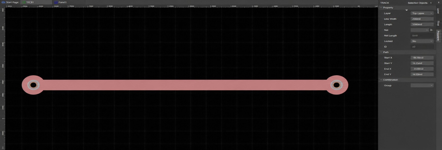
EasyEDA high-current trace width calculator showing copper weight, current, and temperature rise settings for a power PCB layout.
Copper Pour vs. Dedicated Power Planes
Copper pour is useful when a high-current path needs more copper area than a single routed trace can provide. Instead of forcing current through one narrow line, a pour can spread the current across a wider shape and also help move heat away from pads, MOSFETs, connectors, and shunt resistors. This is why copper pours are often used around input terminals, regulator outputs, motor driver paths, and battery connections.
A copper pour still needs to be checked carefully. It can look large on the screen, but the real current may pass through one narrow neck if the pour is connected badly. Small gaps, thin bridges, or thermal relief spokes can create a hidden bottleneck. For heavier current, a dedicated power plane is usually more predictable because it gives the current a wider and more continuous path across the board.
The choice depends on the board size, layer count, current level, and heat target. A two-layer high-current PCB may rely more on wide pours because there are fewer routing options. A four-layer or six-layer board can use a dedicated power plane for cleaner distribution. In both cases, the designer should inspect the actual current path, not just the copper area. The safest layout avoids narrow neck-downs and keeps the power and return paths close enough to reduce voltage drop and EMI.
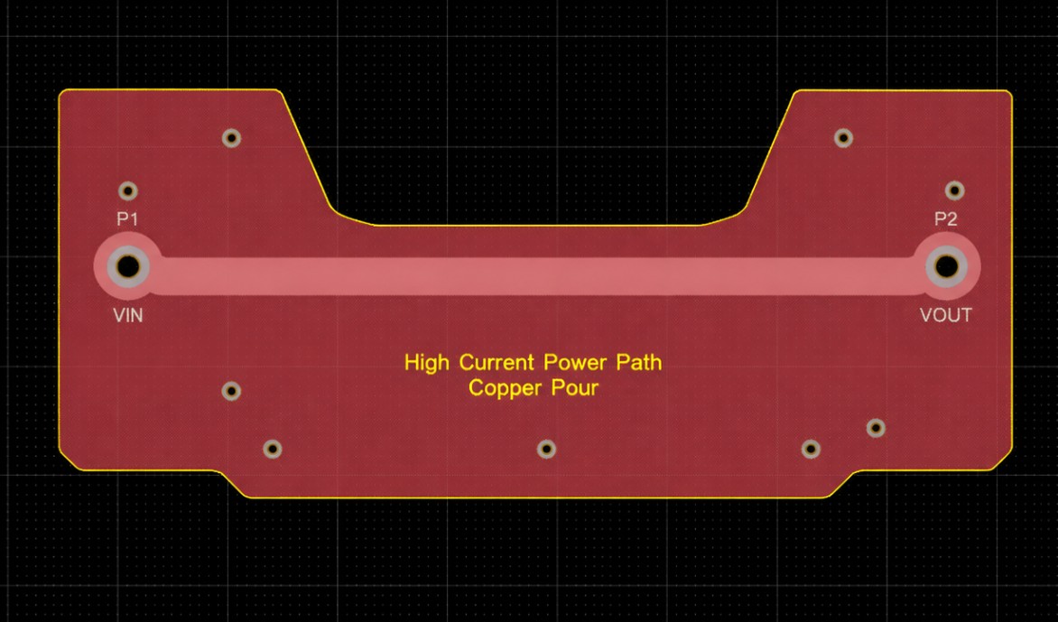
EasyEDA layout showing a large copper pour region used for high-current power distribution on a PCB.
Via Arrays and Kelvin Connections
Via arrays are used when current has to move from one copper layer to another without forcing everything through a single plated hole. In high-current areas, one via may look acceptable on the layout, but it can become a small hot point if the current is high enough. A group of vias spreads the current between several barrels and also helps move heat into the other copper layers.
The placement matters as much as the number of vias. Vias should sit close to the pad, connector, MOSFET drain, shunt resistor, or copper region they are supporting. If the vias are placed far away, the current may still pass through a narrow copper neck before reaching them. That defeats the purpose of the via array.
Kelvin connections are used for measurement, not for carrying load current. For example, a current shunt should have two heavy copper connections for the load path and two separate thin sense traces for voltage measurement. The sense traces should connect directly to the shunt pads, away from the high-current copper. This keeps the measurement more accurate because the controller reads the voltage across the shunt itself, not the extra voltage drop in the power trace.
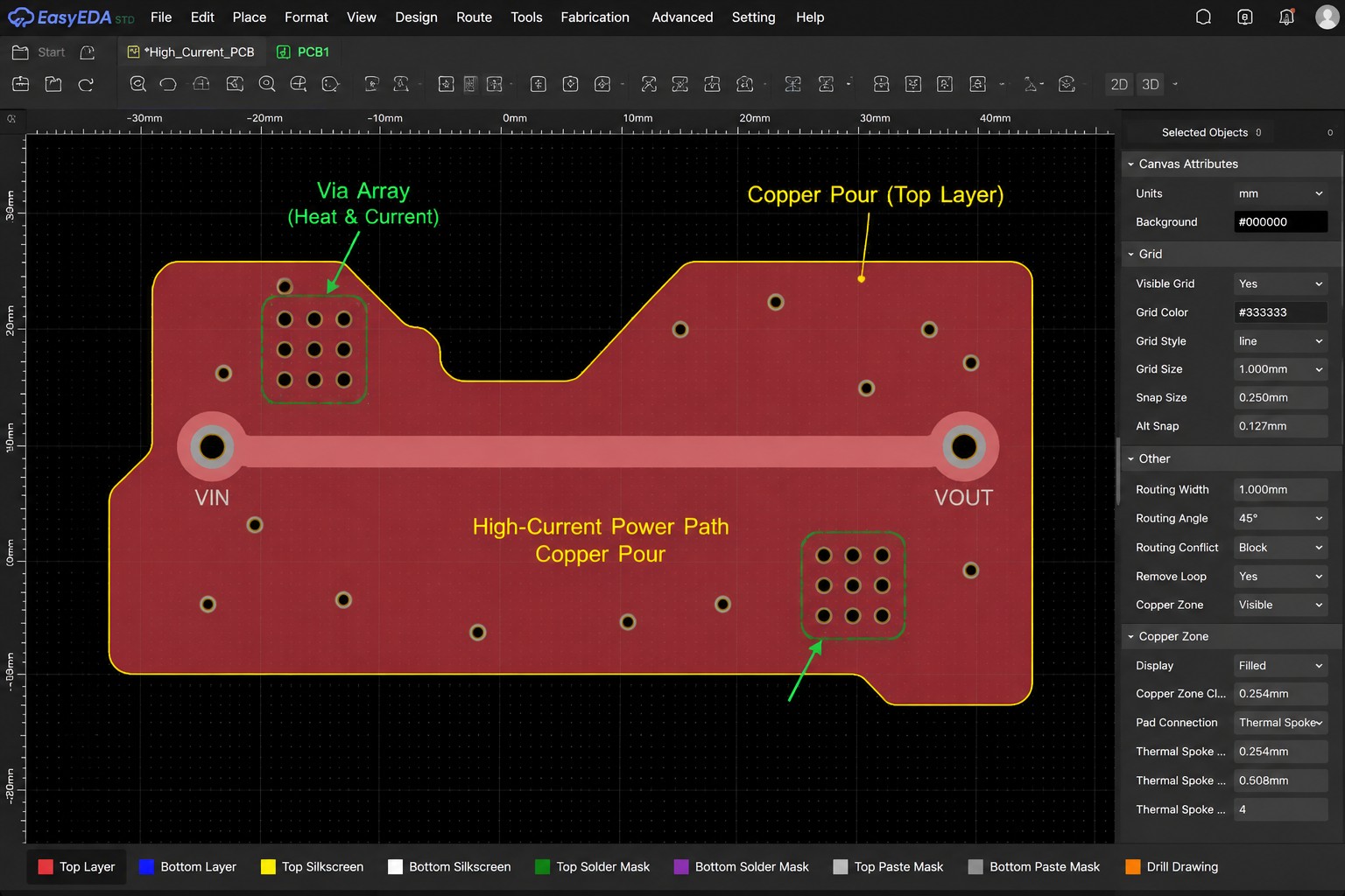
A via array placed in a high-current copper pour region for distributing current across multiple PCB layers.
Thermal Management in High Power PCB Design
Thermal management is where many high power PCB designs prove whether the layout is actually safe. A board may pass a basic electrical check and still fail thermally when it runs at full current for several minutes. Heat does not only come from obvious power components. It can also come from copper neck-downs, vias, connectors, shunt resistors, diodes, and switching devices.
The goal is not just to remove heat after it appears. A better approach is to guide heat away from the beginning by using wider copper, better pad connections, thermal vias, exposed pads, and enough spacing around hot parts. In high power PCB design, thermal decisions should be made during placement and routing, not after the layout is already finished.
Locating and Modeling Thermal Hotspots
Hotspots usually appear where current density and component loss meet. On a high power PCB, the first places to check are MOSFETs, diodes, regulators, current shunts, power resistors, connectors, and any narrow copper section between them. A connector pin, for example, may look harmless in the layout, but it can become one of the warmest points if the current enters the board through a small contact area.
The easiest way to find these risks early is to mark the expected current path before routing is finished. Follow the path from input connector to load, then follow the return path back to the source. Any place where the copper becomes narrow, changes layers, passes through a via group, or reaches a high-loss component deserves attention. For important designs, IR drop and thermal simulation should be used before the first board spin. After assembly, a thermal camera or thermocouple check under full load can confirm whether the model matches the real board.
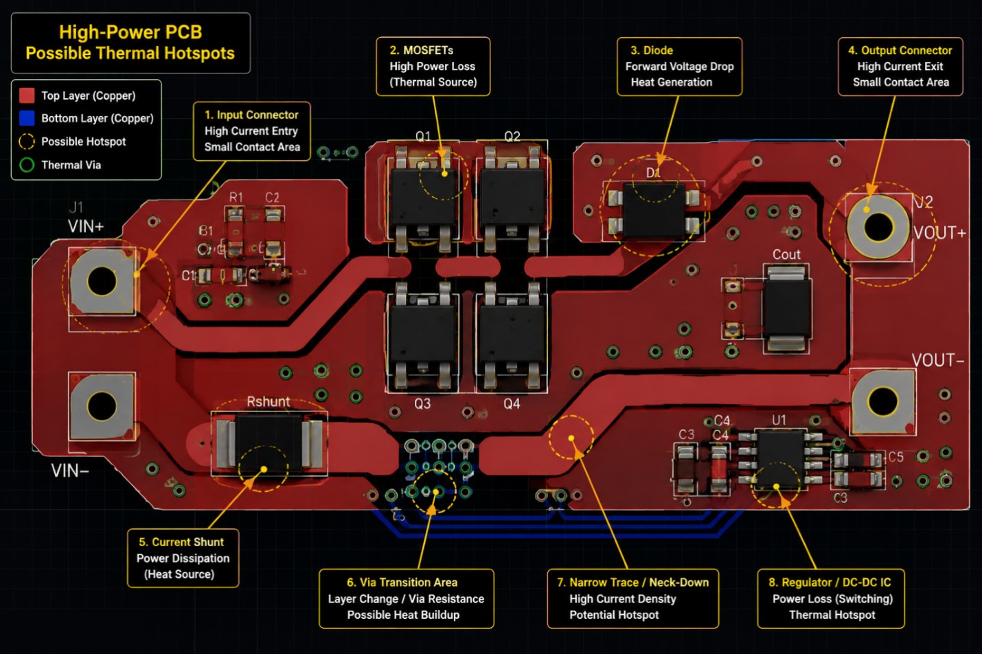
Thermal hotspot map showing temperature distribution across a high-power PCB under load, identifying areas with elevated heat.
Pad Thermal Relief: When to Use, When to Avoid
Thermal relief is useful when a pad needs to be soldered without fighting against a large copper area. The small copper spokes reduce heat flow into the surrounding pour, so the pad reaches soldering temperature faster. For normal signal parts and low-current components, this usually makes assembly easier and more consistent.
In high-current areas, the same feature can become a weak point. A connector pin, MOSFET drain pad, shunt resistor pad, or power terminal often needs a direct low-resistance path into the copper. If the thermal relief spokes are too narrow, the pad may solder nicely, but the current is forced through a few thin copper bridges. That can create local heating around the pad even when the surrounding copper pour looks large.
For power pads, the decision should be made part by part. Signal pads and light-load pads can usually keep thermal relief. High-current pads often need solid copper connection, wider spokes, or multiple copper connections. The right choice depends on soldering method, copper weight, current level, and how much heat the pad is expected to carry during operation.
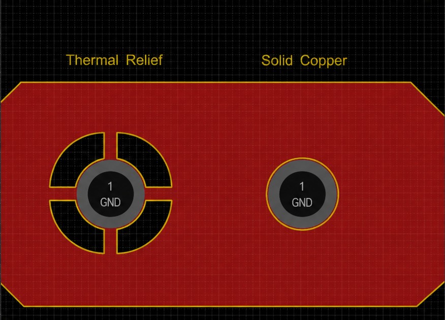
Comparison of thermal relief spoke connection versus solid copper pad connection for high-current PCB pads.
Passive Dissipation Techniques: Spreaders, Slugs, and Exposed Pads
Passive cooling starts with copper. A larger copper area around MOSFETs, regulators, diodes, and shunt resistors helps spread heat before it becomes concentrated in one small location. This does not remove heat by itself, but it lowers the peak temperature and gives the board more surface area to release heat into the air, enclosure, or mounting structure.
Exposed pads are especially important on power ICs and regulators. If a package has an exposed thermal pad, it should not be treated like a normal signal pad. The pad needs enough copper underneath it, and thermal vias can help move heat to the opposite layer or to a larger copper region. When the heat has nowhere to go, the component temperature rises even if the electrical routing looks correct.
For higher-power designs, copper alone may not be enough. Metal slugs, heat spreaders, chassis contact, or external heatsinks may be needed. These features should be planned while placing the components, not after routing is already finished. Once the board is crowded, it becomes much harder to create a clean heat path.
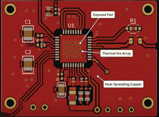
Exposed pad with thermal via arra.
Managing EMI Without Compromising Power Delivery
High current and EMI are closely connected. A board can have enough copper to carry the current but still create noise if the current path is long, poorly returned, or placed near sensitive circuits. The goal is not to make the power path weak just to reduce noise. The goal is to keep current loops compact, return paths predictable, and switching nodes controlled.
In high power PCB design, EMI control should be considered at the same time as copper sizing. A wide trace with a bad return path can still cause problems. A power stage with a large switching node can disturb sensors, communication lines, or control circuits nearby. Good EMI practice keeps noisy current local and prevents it from spreading through the rest of the board.
Minimizing High-Current Loop Area
Loop area matters because current always has two paths: the outgoing path and the return path. If these two paths are far apart, the loop becomes larger and the board can radiate more noise. This is especially common in motor drivers, buck converters, LED drivers, and battery-powered systems where current changes quickly.
A better layout keeps the high-current supply path and return path close together. The input capacitor, switching device, diode or synchronous MOSFET, and load connection should be placed so the main current loop is short and easy to follow. In many layouts, the copper width is enough, but the loop is still too large. That kind of EMI problem is difficult to fix later with only filtering or firmware changes.
Decoupling Strategy and Return Path Control
Decoupling capacitors only work well when they are placed in the real current path. A large capacitor far away from the switching device may look correct in the schematic, but the copper and via inductance between the capacitor and the load can make it much less effective. The input capacitor of a regulator or driver should sit close to the power pins, with a short and direct return to ground.
Return path control is just as important. A broken ground plane, a long via path, or a shared return between power and sensitive signals can allow noise to enter the control circuit. For mixed power and signal boards, high-current return paths should be kept away from ADC references, sensor grounds, communication lines, and clock areas where possible.
Switching Node Containment and Filter Layout
Switching nodes should be kept small because they carry fast voltage transitions. The copper connected to a switching node may not always carry the highest DC current, but it can create strong electric-field noise. If this copper area is made too large, the noise can spread into nearby signals, connectors, or control circuits.
Filters should also be placed where they actually block noise. An input filter should sit close to the connector or the noise entry point. A switching regulator filter should be close to the regulator and the load path it supports. Sensitive traces should not run under inductors, switching nodes, or high-current copper unless there is a controlled reference plane and a clear reason for doing it.
High Current PCB Layout: Simulation, DFM, and Testing
A high current PCB should not go directly from layout to production without checking how it behaves under real load. Visual inspection is useful, but it cannot show every voltage drop, hotspot, or manufacturing risk. Simulation, DFM review, and load testing each catch a different type of problem.
Simulation helps find electrical and thermal weak points before the board is built. DFM review checks whether the board can actually be manufactured and assembled reliably. Testing confirms whether the finished board behaves the way the design expected. For high-current work, all three steps matter.
IR Drop and Thermal Simulation Before First Spin
IR drop simulation shows where voltage is lost along the copper path. This is useful because the schematic may show one clean power net, while the layout creates many small resistive sections. A thin neck near a connector, a weak via transition, or a long return path can reduce the voltage that reaches the load.
Thermal simulation adds another layer of checking. It helps show whether heat is spread across the board or concentrated at one pad, trace, connector, or component. The simulation does not need to be perfect to be useful. Even a simple model can show which parts of the layout need more copper, more vias, or a different placement before the first prototype is ordered.
DFM Considerations Specific to High-Current Boards
High-current boards create DFM challenges that may not appear in small-signal designs. Heavy copper can affect minimum spacing, etching accuracy, drill requirements, solder mask openings, and pad geometry. A layout can look simple electrically but still be difficult to manufacture if the copper is too thick for the selected spacing or if the via plating requirements are not realistic.
Connectors, terminal blocks, and large pads should also be checked from an assembly point of view. A high-current pad with a solid copper connection may be electrically strong, but it can be harder to solder. A pad with too much thermal relief may solder easily, but it can limit current. This is why DFM review should include copper weight, spacing, via structure, pad connection style, solderability, and expected temperature rise.
Validation: Load Testing and Thermal Mapping
The final check is real load testing. A prototype should be tested at the expected operating current, not only powered briefly on the bench. The test should include full-load operation, startup current, worst-case duty cycle, and expected ambient temperature. If the product will run inside an enclosure, the test should include that enclosure or a similar thermal condition.
Thermal mapping is one of the most useful checks. A thermal camera can quickly show hot connectors, narrow traces, overloaded vias, and components that are heating nearby copper. Thermocouples are also useful for checking specific parts over time. The important point is to compare the test result with the design expectation. If one area is hotter than expected, the layout should be corrected before production.
FAQ about High Current PCB Design
What Is Considered a High Current PCB?
A high current PCB is a circuit board designed to carry significantly more current than a typical signal board. Instead of focusing only on electrical connections, the layout must also manage voltage drop, heat generation, copper resistance, and long-term reliability. There is no single current value that defines a high current PCB because it depends on copper weight, trace width, layer count, operating temperature, and duty cycle. A board carrying only a few amps may already require high-current design practices if the available space is limited or the product operates continuously. In practice, a PCB should be treated as a high-current design whenever current flow becomes an important part of the electrical and thermal design rather than just the schematic.
Is 1 oz Copper Enough for High Current PCB Design?
1 oz copper can be enough for some high current PCB design cases, but only when the current path is short, wide, and not running close to the thermal limit. It is commonly used because it is affordable and easy to manufacture, but it does not automatically provide enough margin for continuous high-current loads.
For currents above 10 A, especially in enclosed products or boards with limited airflow, 2 oz or 3 oz copper is often a safer choice. The final decision should depend on trace width, temperature rise, copper area, current duration, and manufacturing limits.
Can Vias Carry High Current Safely?
Vias can carry current safely, but they should not be treated like ideal copper connections. A single via has limited plated copper area, so it can become a hot spot if too much current is forced through it. This is especially important when current moves between layers near connectors, MOSFETs, shunts, regulators, or battery paths.
For high-current layer changes, via arrays are safer than single vias. Several vias placed close to the power pad or copper region allow current to split between multiple barrels, reducing local heating and voltage drop.
Why Does a Connector Get Hot Even When the Trace Is Wide?
A connector can get hot because the current still has to pass through the metal contact, screw terminal, crimp, or solder joint. The PCB trace may be wide enough, but the connector contact may have higher resistance than expected.
This resistance can look very small on paper, but it matters at high current. For example, a few milliohms can create noticeable heat when the current is 10 A, 20 A, or more. That is why connector current rating, contact resistance, wire size, terminal pressure, and temperature rise should all be checked before production.
Should Thermal Relief Be Used on High-Current Pads?
Thermal relief is useful for soldering because it stops a large copper area from pulling heat away from the pad too quickly. For signal pads and low-current components, this is usually helpful.
For high-current pads, thermal relief can become a weak point if the spokes are too thin. Connector pins, MOSFET drain pads, current shunts, and power terminals often need a stronger copper connection. In those cases, solid copper, wider spokes, or multiple copper connections may be better. The choice should balance solderability, current capacity, heat spreading, and assembly method.
How Can High Current PCB Layout Be Checked Before Production?
A high current PCB layout should be checked in several ways before production. First, trace width and copper weight should be reviewed against the expected current and temperature rise. Then the layout should be inspected for narrow neck-downs, weak via transitions, broken return paths, and hot connector areas.
For important designs, IR drop and thermal simulation should be done before ordering prototypes. After assembly, the board should be tested at real load using a thermal camera or thermocouples. This final test is important because real airflow, enclosure conditions, connectors, and component heating can change the result compared with the layout calculation.
Conclusion: High Current PCB Design
High Current PCB Layout is not solved by one wide trace, one copper pour, or one calculator result. A reliable power board comes from many small decisions working together: correct copper weight, wide current paths, strong via arrays, low-resistance connectors, continuous return paths, controlled EMI loops, and realistic thermal planning.
The best results come when current flow is considered from the beginning of the design, not only after routing is complete. A high power PCB should be checked for voltage drop, heat buildup, manufacturability, and real load behavior before production. When these steps are followed, the board is more likely to operate safely, stay stable under load, and avoid expensive redesign after the first build.
Keep Learning
Bypass Capacitor Placement in PCB Layout: Best Practices
Quick answer:Bypass Capacitor Place each bypass capacitor as close as possible to the IC's power and ground pins, connect it with short, wide traces, and drop dedicated vias to the power and ground planes right at the capacitor pads — never between the IC and the capacitor. Every millimeter of trace adds roughly 1 nH of parasitic inductance, which raises the loop impedance (Z = 2πfL) and defeats the capacitor at high frequencies. The smaller the capacitor value, the closer it must sit to the pin. Intr......
Track Width v/s Current Capacity: PCB Layout Tips for Power Routing
Key Takeaways Trace width and copper thickness set the current limit. Standard 1 oz (35 µm) copper suits most designs; step up to 2–3 oz for power-hungry boards. Size traces against IPC-2221/IPC-2152 for a safe temperature rise. Internal layers carry less current than external ones. Buried traces dissipate heat poorly, so derate them or move high-current paths to outer layers. Vias are a bottleneck—each carries only about 500 mA. When routing power across layers, stitch multiple vias in parallel rathe......
Circuit Board Ground Plane and Power Plane Guide 2026
Key Takeaways Continuous copper first: A solid circuit board ground plane creates a low-impedance return path, reduces noise, and is usually safer than split planes, even on mixed-signal boards. Think in current loops: Every signal needs a return path directly beneath it. Never route high-speed traces across plane gaps, slots, or cutouts. Plan the stack-up early: Choose the layer arrangement before routing critical signals, and keep power and ground planes close together to lower distribution inductan......
Guide to Ground Bounce in PCB - Causes, Effects & Prevention
Key Takeaways Ground bounce is a voltage spike between an IC's die ground and the PCB ground. It happens when current changes fast through parasitic inductance (V = L x di/dt). Many outputs switching at once, called SSO, make it much worse. It can cause logic errors, false resets, and ringing on signals. You measure it with a quiet-low sense line on a scope. Good decoupling, short ground loops, and slower slew rates fix most of it. Introduction A board passes every test on the bench. Then, in the fiel......
Voltage Regulator PCB: Practical Design Guide
Key Takeaways A voltage regulator PCB doesn't just convert one voltage into another; it must also provide a stable output while handling heat, load changes, and noise in the circuit. The layout is as important as the regulator IC; keep the input and output capacitors near the pins, use short power connections, and ensure a direct, low-impedance ground return. Linear regulators are simple and quiet, but they lose voltage difference as heat; switching regulators are the better option when the voltage dr......
LDO vs Switching Regulator: Comparison & PCB Layout
Key Takeaways Calculate LDO dissipation first: Always calculate LDO power dissipation at maximum input voltage and load before comparing packages or prices. Condition-dependent specs: Treat dropout, PSRR, noise, ripple, efficiency, and transient response as condition-dependent, not fixed values. Layout matters for both: A buck converter's high-di/dt input loop and high-dv/dt switch node create different coupling mechanisms. Both need deliberate PCB placement. Output capacitor selection: The output cap......