Understanding Star Grounding in PCB Design: A Practical Guide
16 min
- Introduction
- What Is Star Grounding in PCB Design?
- Key Advantages and When to Use Star Grounding
- Star Ground vs. Ground Plane — Making the Right Choice
- Star Grounding PCB Layout — Step-by-Step Guide
- Common Star Grounding Mistakes and How to Avoid Them
- FAQ about Star Grounding in PCB Design
Key Takeaways
Controlled Return Paths: Star grounding gives selected circuit blocks separate return paths that meet at one controlled physical point. It limits shared-impedance coupling between noisy and sensitive sections.
Best Applications: It works best in compact, low-frequency, low-current, or noise-sensitive systems, including audio stages, sensor interfaces, and selected precision circuits.
Ground Plane Alternative: A ground plane provides a broad, low-inductance reference that is normally better for fast digital signals, RF, and complex mixed-signal boards.
Layout Discipline: Keep every star branch short, wide, and dedicated, and permit the branches to touch only at the intended star ground point.
Avoid Over-Application: Do not apply star grounding blindly to USB, Ethernet, DDR, RF, or fast clocks. These signals need a continuous nearby return path.
Never Cross Gaps: Never route a signal across a gap between ground regions. Doing so enlarges the return loop and can create serious EMI and signal-integrity problems.
Introduction
A PCB can pass every design-rule check and still fail on the bench. The ADC value jumps whenever the display updates. An audio channel develops a low hum. A motor driver causes the microcontroller to reset. The schematic looks correct, the power rails measure properly, and no track is visibly broken—yet the board behaves unpredictably. In many cases, the missing piece is not another capacitor or firmware filter. It is the return-current strategy. Star grounding is one of the first techniques designers encounter when trying to solve that problem, but it is also one of the most frequently misunderstood.
Ground is not a magical sink that absorbs current. Every signal and every power rail forms a complete loop, and the layout determines where the return portion of that loop travels. A successful PCB star grounding strategy therefore begins with current paths, not with drawing a star-shaped collection of traces.
This guide explains what star grounding means electrically, where it remains useful, when a ground plane is the better choice, how to build a practical layout in EasyEDA , and which mistakes can turn a neat-looking ground system into an EMI problem.
What Is Star Grounding in PCB Design?
Star grounding is a single-point topology that originated in system wiring, instrumentation, and audio design. On a PCB, it is useful only when the designer can control the relevant return paths and keep them short.
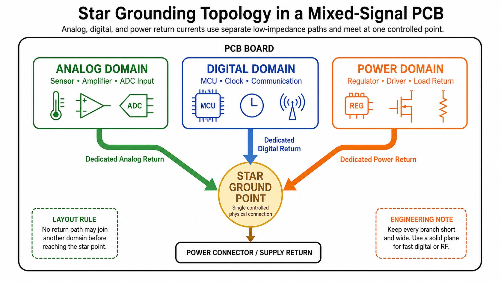
Figure 1. Dedicated analog, digital, and power returns converge at one controlled star point.
The Core Concept — Single-Point Grounding Explained
Imagine several roads leading to one roundabout. Traffic from each neighborhood reaches the junction without first passing through another neighborhood. In a circuit, the neighborhoods are functional blocks, the roads are ground conductors, and the roundabout is the star ground point.
A board may contain a sensitive analog front end, a microcontroller, and a power stage. In a true star arrangement, the analog, digital, and power returns use dedicated conductors that meet at exactly one deliberate location—often near the main supply return, a bulk capacitor, or another reference node selected from the circuit's current paths.
The topology resembles a star, but the shape is not the real objective. The purpose is to stop a large or noisy current from flowing through copper that also defines the reference for a sensitive circuit. If an LED driver and sensor amplifier share a thin return track, the driver's pulsed current creates a voltage along that track. The ADC then sees a disturbed sensor reference. A dedicated branch can reduce that coupling, provided both the outgoing and return paths remain compact.
This is the practical meaning of star grounding in PCB design: intentional control of shared impedance, not simply routing every GND pin to a distant central pad.
How Star Grounding Controls Return Current Paths
Every current leaves a source, passes through a load, and returns to the source. The return conductor is therefore part of the circuit, even when the schematic reduces it to a GND symbol.
PCB copper has resistance and inductance. Current flowing through that impedance develops a voltage. At DC and very low frequencies, V = I × R explains much of the effect. As frequency rises, trace inductance becomes increasingly important, so a conductor that appears excellent at DC may become a poor high-frequency reference.
If a regulator, MCU, and precision sensor share one narrow ground path, regulator pulses and MCU edges shift the sensor and ADC reference. A star system gives each selected block a separate route to a low-impedance common node, so the power branch's voltage drop does not appear directly in the analog branch.
This works best when currents are slow enough for the routed network to behave predictably. At high frequencies, return current seeks the path of least impedance, normally close to the signal trace. Long radial branches then become inductive and increase loop area, which is why fast signals usually require a continuous ground plane.
Key Advantages and When to Use Star Grounding
Star grounding is not a universal cure. It is effective only when current paths are simple, circuit blocks are compact, and cross-domain signals can be controlled.
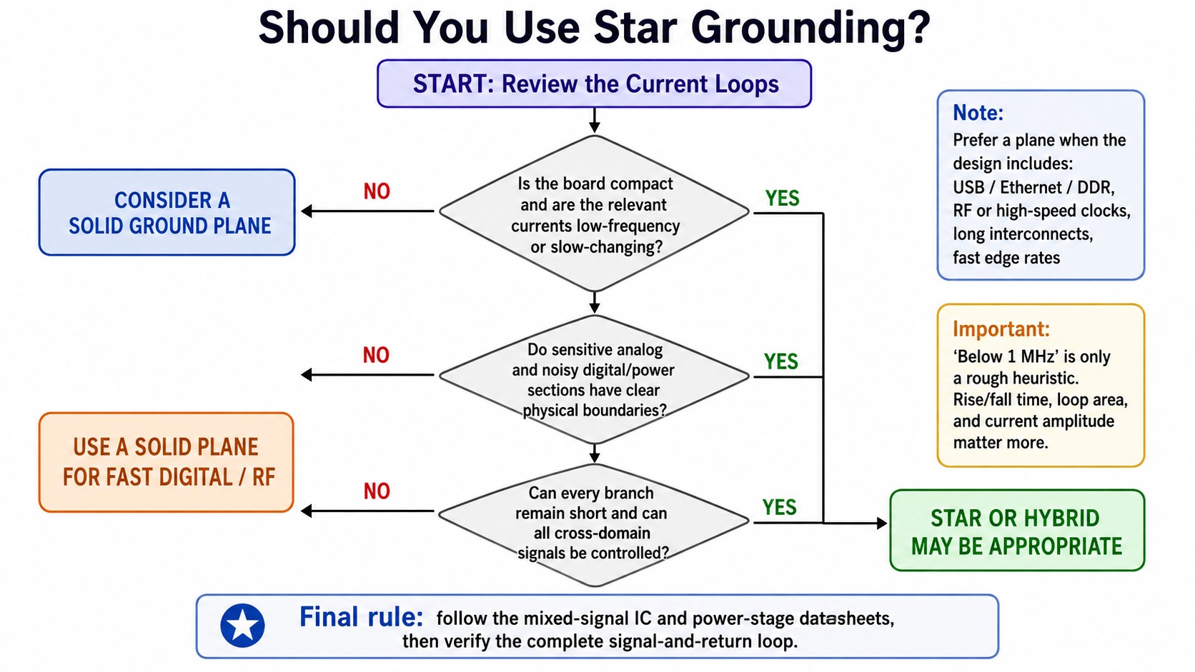
Figure 2. Decision flowchart for selecting star grounding, a hybrid strategy, or a solid ground plane.
When Star Grounding Works Best
Consider it when several of these conditions are true:
- Currents are DC or low frequency. Audio stages, bridge sensors, slow control loops, and precision measurement circuits can benefit from having their returns explicitly separated.
- The PCB is compact. Short branches remain lower in resistance, inductance, and loop area than branches stretched across a large board.
- Domains are physically clear. Sensitive analog, low-speed digital, and noisy power sections can be clustered without signals repeatedly crossing boundaries.
- One block carries much higher current. Relays, motors, lamps, speakers, and converters should not share sensitive reference copper.
- The component datasheet recommends a single-point connection. Device-specific guidance always outranks a generic grounding rule.
Note
"Below about 1 MHz" is only a screening aid. A 100 kHz square wave with a fast edge contains high-frequency energy. Judge the layout by edge rate, loop area, current magnitude, and required noise performance.
Avoid radial stars for USB, Ethernet, DDR, RF, fast clocks, and any design where signals must cross separated reference regions. These applications normally need a solid plane.
Real-World Example — Sensor + MCU Mixed-Signal Board
Consider a compact monitor with an analog sensor interface, ADC, MCU, and switching regulator. The sensor needs a quiet reference; the MCU creates repetitive switching current; and the regulator carries pulsed power current.
In a poor layout, the regulator, MCU, and sensor grounds are daisy-chained. Regulator and MCU current then develops a voltage in the same copper used by the sensor and ADC, producing noisy readings.
A controlled PCB star grounding layout gives the sensor path an analog branch, the controller a digital branch, and the regulator and load a power branch. They meet at one selected low-impedance node. The benefit comes from preventing high di/dt power current from sharing the sensor reference—not from the AGND, DGND, and PGND labels themselves.
Tip
If the MCU-to-ADC interface has fast edges, it still needs a continuous nearby return. Place the ADC at the domain boundary and follow its datasheet. Many modern converters work better over one continuous plane with disciplined placement than over physically split grounds.
Star Ground vs. Ground Plane — Making the Right Choice
Star networks explicitly assign conductors to circuit blocks. Ground planes instead provide a broad, low-impedance reference that allows high-frequency return current to remain close to its signal path.
How Ground Planes Work and Why They Are the Modern Standard
A ground plane is a continuous copper area, ideally on an uninterrupted PCB layer. Its large area lowers impedance, while its proximity to signal traces lets high-frequency return current flow directly beneath or near those traces.
At low frequency, return current is influenced mainly by resistance. As frequency rises, inductance and magnetic coupling dominate, so the preferred path is the one that minimizes loop area. A continuous plane supports that path automatically.
The signal conductor and its return form a loop. Increasing their separation increases radiation, susceptibility, and crosstalk. A trace routed over an unbroken plane has a compact loop; a trace crossing a split forces its return to detour through a distant connection or stray capacitance.
This is why a plane is the default for fast digital designs and many mixed-signal boards. Rather than cutting the plane, group analog parts in one area, digital parts in another, place the converter at the boundary, and route each signal so its return stays within the intended zone. This partitions current through placement and routing instead of through a gap in the reference.
For a deeper look at plane continuity, return-path planning, and stack-up selection, see our Circuit Board Ground Plane and Power Plane Guide.
Comparison Table — Star Ground vs. Ground Plane
| Feature | Star Ground | Ground Plane | Notes |
|---|---|---|---|
| Topology | Single-point radial branches | Continuous copper reference | Hybrid layouts may use both locally |
| Best use | DC, audio, slow control, selected precision analog | General-purpose, fast digital, RF, mixed-signal | Frequency alone is not decisive |
| Return-path control | Designer defines each branch | High-frequency return follows the signal | Both need disciplined placement |
| EMI performance | Can be poor with long branches | Usually excellent with an unbroken plane | Never cross a split with a fast trace |
| Layout complexity | High | Moderate | Planes scale more easily |
| Typical applications | Audio, instrumentation, sensors, power-return isolation | MCU, high-speed digital, RF, general mixed-signal | Datasheet guidance has priority |
The practical star ground vs. ground plane rule is straightforward: use controlled single-point returns when currents are slow, the board is compact, and shared impedance is the main concern. Use a plane when signals have fast edges, the board is large, or many interconnections need a continuous reference.
Professional boards often use a hybrid. A solid plane supports digital and general return currents, while a shunt amplifier, audio input, power stage, or precision reference uses a local Kelvin or single-point connection.
Star Grounding PCB Layout — Step-by-Step Guide
EasyEDA supports net-assigned tracks, copper areas, solid regions, design rules, and DRC. Use these features to make the intended return architecture visible and verifiable.
1Identify the Domains
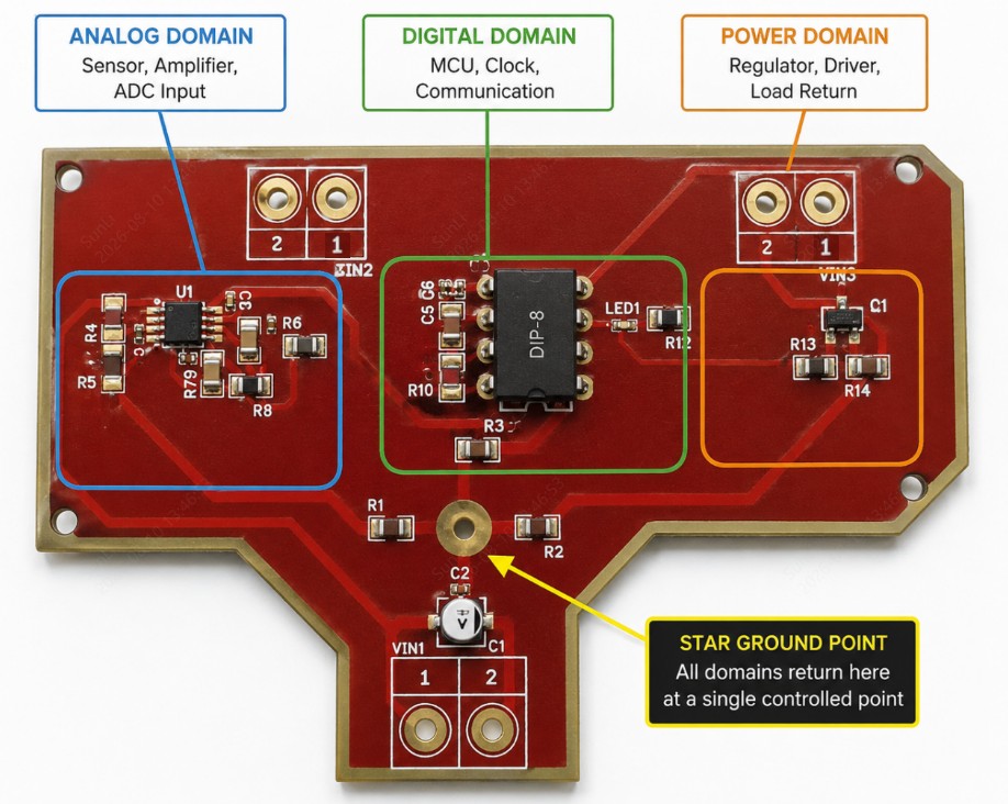
Figure 3. PCB layout classifying analog, digital, and power domains by current behavior before star ground routing begins.
- Analog/sensitive: sensors, op-amps, references, ADC inputs, low-level audio.
- Digital/noisy: MCU, clocks, memories, logic, displays, communication interfaces.
- Power/very noisy: switching regulators, drivers, motors, relays, LEDs, speakers, and other high-current loads.
Place each block as a compact cluster and mark its boundary on a documentation layer. Trace every important current loop from source to load and back. Classify components by the current they conduct, not merely by their names; an ADC is mixed-signal, and a regulator feedback divider is sensitive.
2Choose the Star Point
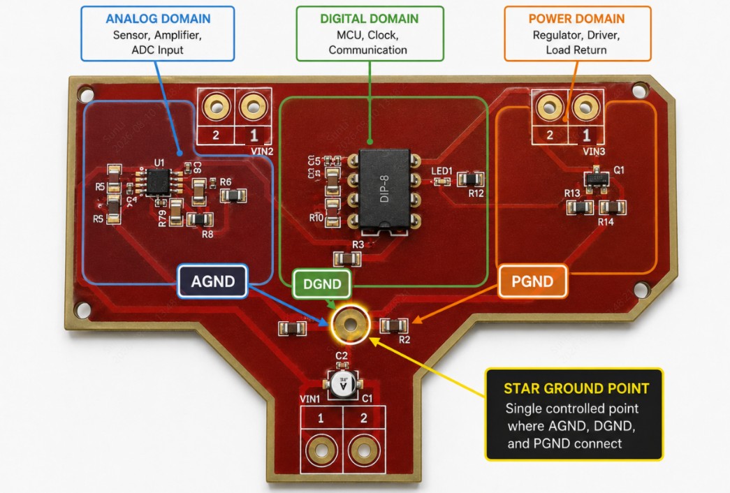
Figure 4. Star ground point placed near the main supply return with short branches connecting analog, digital, and power sections.
Choose the star point after examining the loops. It should be close to the main supply return or the node specified by the relevant datasheet, built with a broad pad or solid copper region, and located so every branch remains short.
Do not place it at a remote board edge, behind a narrow copper neck, or wherever routing happens to be convenient. In an audio amplifier it may be near the reservoir capacitor return; in an ADC circuit it may be at or beneath the converter.
3Route the Ground Branches
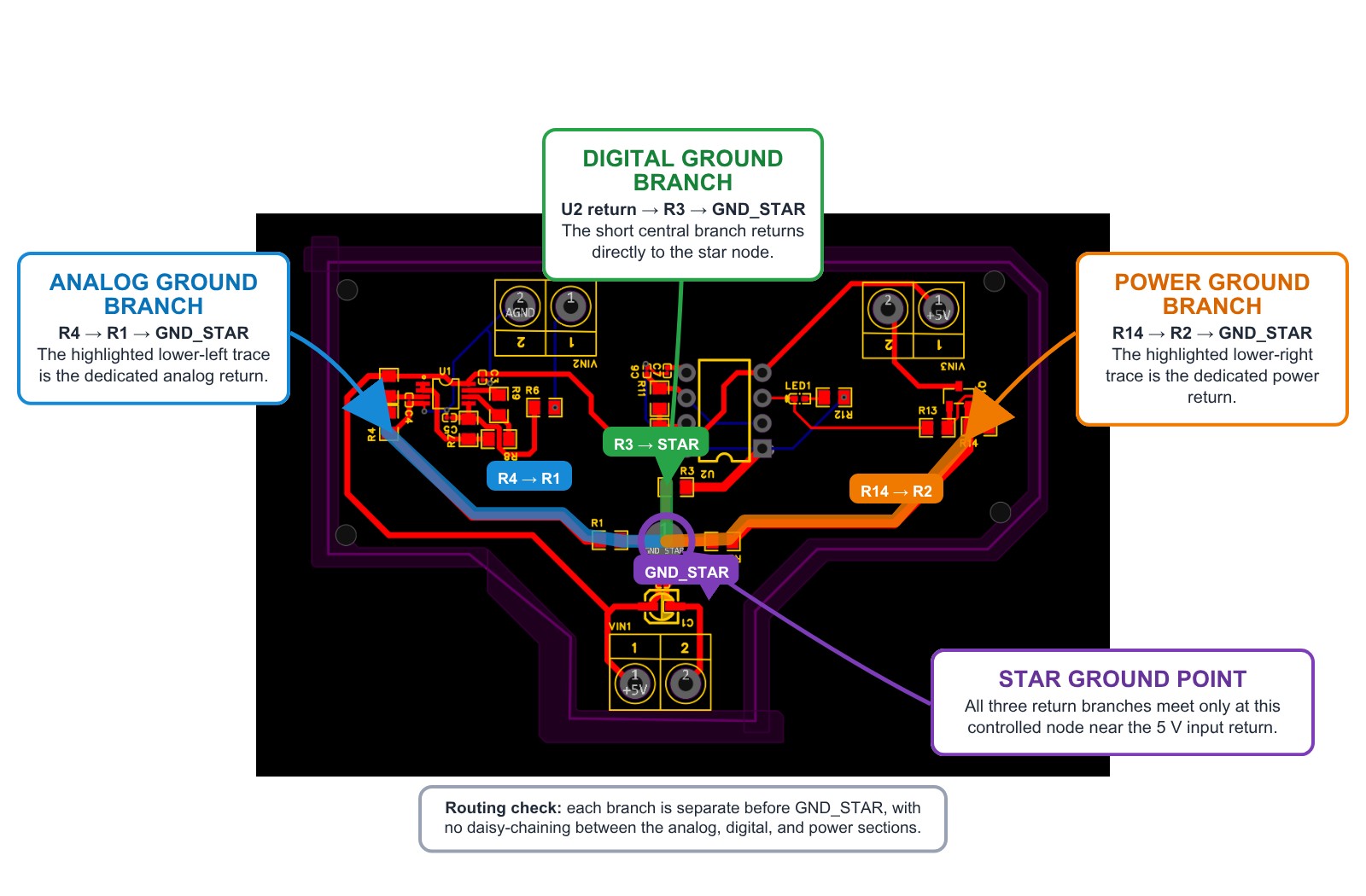
Figure 5. Ground branches routed from the star point to each domain with analog first, digital second, and power last, kept short and wide.
Route analog first, then digital, then power. Keep each branch short, wide, and direct. A width of 1 mm or more is a useful visual starting point for low-current examples, but high-current copper must be calculated from copper thickness, temperature rise, and acceptable voltage drop.
Do not daisy-chain one block through another. Keep the outgoing signal or supply conductor close to its return; a wide ground track cannot compensate for a large loop.
4Verify Isolation
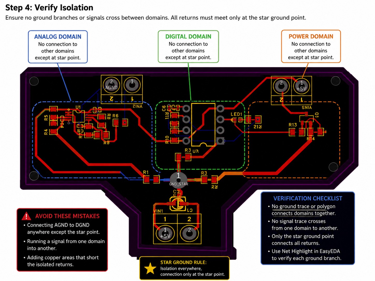
Figure 6. Checking isolation of star ground branches by hiding nonessential layers and inspecting copper connections at high zoom.
Hide nonessential layers, rebuild all copper, and inspect at high zoom. Confirm that the branches touch only at the intended point and that vias, mounting holes, connector shells, thermal pads, test points, or same-net pours have not created a second connection.
Assign each EasyEDA copper area to the correct net, rebuild it after every important change, and remove unexplained floating copper.
5Handle Mixed-Signal ICs
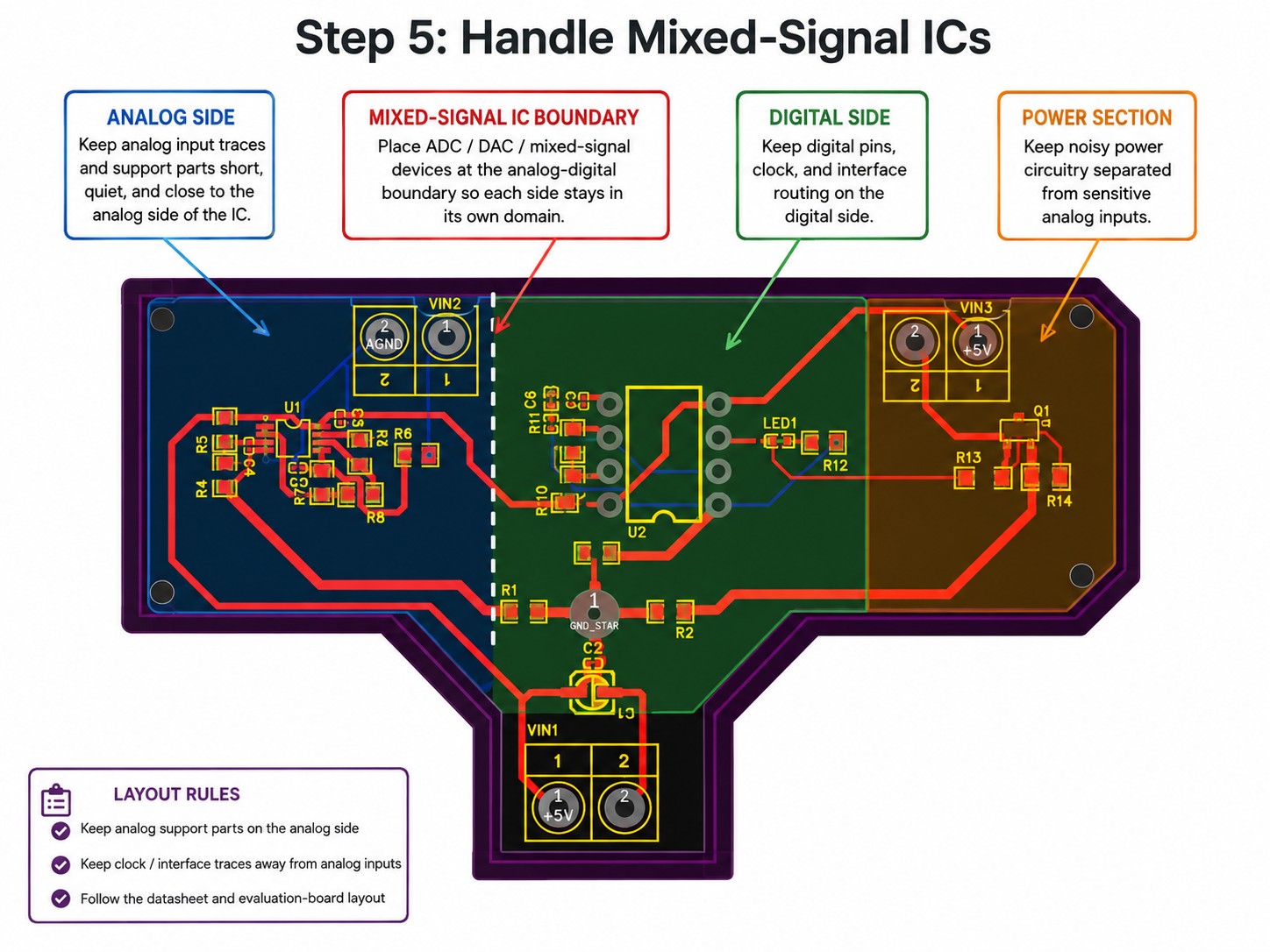
Figure 7. Mixed-signal IC placement at the analog-digital boundary with analog pins on one side and digital pins on the other.
Place an ADC, DAC, codec, or mixed-signal sensor at the analog–digital boundary. Keep analog pins and support parts on the analog side and digital pins on the digital side. Keep clock and interface traces away from the input network.
Follow the exact device datasheet and evaluation-board layout. Some ICs require AGND and DGND to join directly under the package and connect to one plane; others require a different arrangement. A generic diagram cannot replace the manufacturer's guidance.
6Run the Final DRC and Return-Path Review
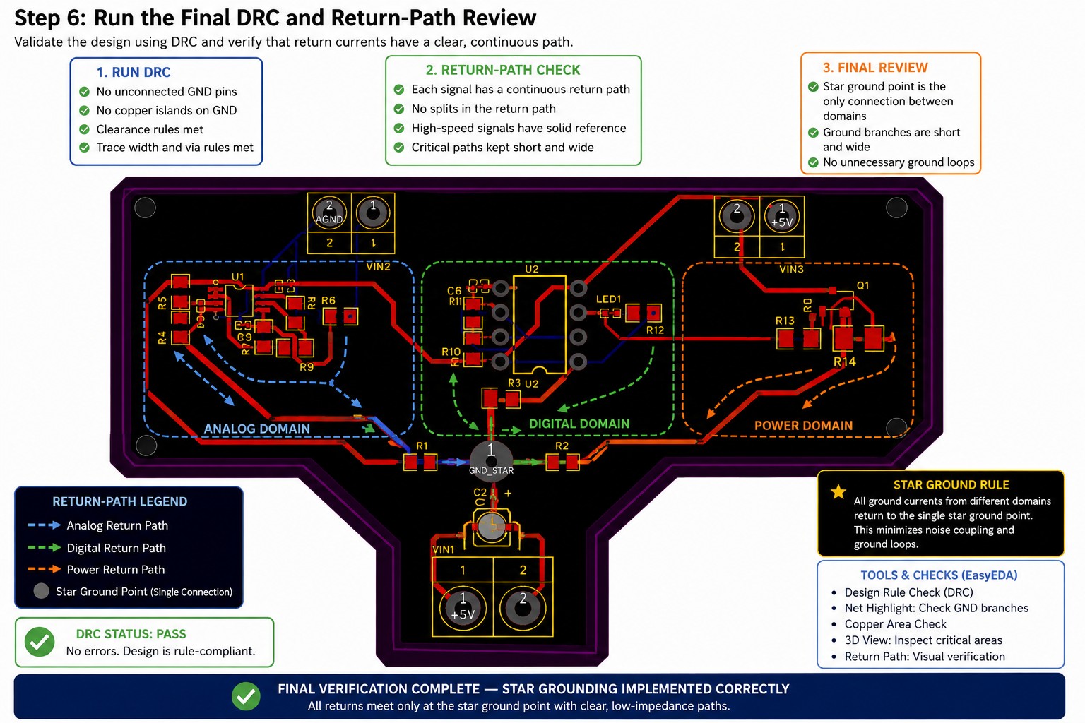
Figure 8. Final DRC and engineering review of star ground layout checking branch current capacity, return paths, and copper integrity.
Run DRC, then perform an engineering review for:
- branch and via current capacity;
- exactly one intended domain connection;
- adequate copper clearance;
- no fast signal crossing a reference gap;
- short IC decoupling loops;
- direct load and bulk-capacitor returns;
- connector, shield, and chassis grounding;
- an accessible test point at the star node.
On multilayer boards, a hybrid is often best: retain a continuous plane for fast signals and use local Kelvin, power-island, or single-point connections only where required. Star grounding in PCB design should be intentional and local, not a decorative pattern imposed across the board.
Common Star Grounding Mistakes and How to Avoid Them
These errors often pass schematic review and DRC because every net is technically connected. They are current-path and electromagnetic problems that require reviewing the complete signal-and-return loop.
Routing Signals Across Ground Domain Gaps
A signal cannot travel without a return. When a trace crosses between separated ground regions, its return current cannot remain beneath it. The current must detour through a distant star point, cable shield, or stray capacitance, increasing loop area and inductance.
The enlarged loop can radiate, receive interference, create crosstalk, and disturb the signal reference. A narrow split can behave like a slot radiator when a fast signal crosses it.
Route each signal over its own continuous reference. Keep analog traces in the analog area and digital traces in the digital area. When a signal must cross domains, make the transition at the converter placed on the boundary. An ADC's analog input should remain over the analog reference, while its digital output should immediately enter the digital region.
Note
A net tie controls the CAD connection but does not guarantee a short high-frequency return path. Placement and routing must make the physical transition compact.
Creating Antenna Loops with Excessively Long Ground Traces
A visually perfect star can still be electrically poor. Several-centimeter spokes have inductance in the tens-of-nanohenries range, depending on their geometry and reference environment. During fast current transitions, $V = L \times di/dt$ produces a ground disturbance, while the enlarged loop increases emissions and susceptibility.
Keep branches short, place related blocks closer to the star point, and route supply and return together. Widening a long trace does not fully solve its loop-area problem.
This is where the star ground vs. ground plane choice becomes practical. On a large or interconnect-heavy PCB, a partitioned layout over a continuous plane is usually better than long radial traces. Reserve single-point and Kelvin connections for local current-sense, audio, power, and precision-reference paths.
FAQ about Star Grounding in PCB Design
Q: What Is a Star Ground Point?
A star ground point is the one physical node where selected, otherwise separate return branches connect. It should be low impedance, mechanically reliable, and located according to the actual current loops—not simply at the geometric center of the PCB.
Q: Is Star Grounding Better Than a Ground Plane?
Not universally. Star grounding can control shared impedance in compact, low-frequency systems, while a continuous ground plane is generally better for fast digital, RF, and complex mixed-signal layouts because it minimizes return-loop area.
Q: Where Should Analog and Digital Grounds Connect?
The correct location depends on the converter and the system architecture. With some ADCs or DACs, AGND and DGND connect together at or beneath the device; with others, a continuous plane and careful partitioning are recommended. Always follow the component datasheet and evaluation-board layout.
Q: Can I Use Star Grounding on a Breadboard?
A star grounding breadboard arrangement can reduce shared return resistance in slow analog or audio experiments. Breadboards still have long conductors, contact resistance, parasitic capacitance, and poor high-frequency behavior, so success on a breadboard does not prove that the same topology is suitable for a production PCB.
Q: Does Star Grounding Eliminate Ground Loops?
It can prevent some unintended shared paths in simple systems, but it does not automatically eliminate every ground-loop or enclosure-current problem. Multiple chassis connections, cable shields, test equipment, and off-board supplies can create additional paths outside the PCB.
Conclusion: Star Grounding in PCB Design
Star grounding is powerful when used for the problem it actually solves: controlling shared return-path impedance in compact, low-frequency, noise-sensitive circuits. It is not a universal replacement for a ground plane, and it should never be applied without tracing the complete current loops.
The strongest PCB layouts begin with intentional placement and grounding architecture. Sensitive analog circuitry is grouped together, noisy power loops are kept compact, digital return paths remain continuous, and mixed-signal devices are handled according to their datasheets. Only then should the designer decide whether a single-point branch, continuous plane, Kelvin connection, or hybrid structure is appropriate.
When applied carefully, star grounding can protect low-level measurements and prevent high-current stages from disturbing sensitive references. When over-applied, it creates long inductive traces and broken return paths.
For designers working on mixed-signal, analog, or noise-sensitive hardware, JLCPCB's PCB layout services can provide professional support so the grounding and return-current strategy is planned correctly before the board reaches fabrication.
Editorial note: The frequency figures in this article are practical screening aids, not absolute boundaries. Final grounding decisions should follow component datasheets and complete return-current analysis.
Keep Learning
Bypass Capacitor Placement in PCB Layout: Best Practices
Quick answer:Bypass Capacitor Place each bypass capacitor as close as possible to the IC's power and ground pins, connect it with short, wide traces, and drop dedicated vias to the power and ground planes right at the capacitor pads — never between the IC and the capacitor. Every millimeter of trace adds roughly 1 nH of parasitic inductance, which raises the loop impedance (Z = 2πfL) and defeats the capacitor at high frequencies. The smaller the capacitor value, the closer it must sit to the pin. Intr......
Track Width v/s Current Capacity: PCB Layout Tips for Power Routing
Key Takeaways Trace width and copper thickness set the current limit. Standard 1 oz (35 µm) copper suits most designs; step up to 2–3 oz for power-hungry boards. Size traces against IPC-2221/IPC-2152 for a safe temperature rise. Internal layers carry less current than external ones. Buried traces dissipate heat poorly, so derate them or move high-current paths to outer layers. Vias are a bottleneck—each carries only about 500 mA. When routing power across layers, stitch multiple vias in parallel rathe......
Circuit Board Ground Plane and Power Plane Guide 2026
Key Takeaways Continuous copper first: A solid circuit board ground plane creates a low-impedance return path, reduces noise, and is usually safer than split planes, even on mixed-signal boards. Think in current loops: Every signal needs a return path directly beneath it. Never route high-speed traces across plane gaps, slots, or cutouts. Plan the stack-up early: Choose the layer arrangement before routing critical signals, and keep power and ground planes close together to lower distribution inductan......
Guide to Ground Bounce in PCB - Causes, Effects & Prevention
Key Takeaways Ground bounce is a voltage spike between an IC's die ground and the PCB ground. It happens when current changes fast through parasitic inductance (V = L x di/dt). Many outputs switching at once, called SSO, make it much worse. It can cause logic errors, false resets, and ringing on signals. You measure it with a quiet-low sense line on a scope. Good decoupling, short ground loops, and slower slew rates fix most of it. Introduction A board passes every test on the bench. Then, in the fiel......
Voltage Regulator PCB: Practical Design Guide
Key Takeaways A voltage regulator PCB doesn't just convert one voltage into another; it must also provide a stable output while handling heat, load changes, and noise in the circuit. The layout is as important as the regulator IC; keep the input and output capacitors near the pins, use short power connections, and ensure a direct, low-impedance ground return. Linear regulators are simple and quiet, but they lose voltage difference as heat; switching regulators are the better option when the voltage dr......
LDO vs Switching Regulator: Comparison & PCB Layout
Key Takeaways Calculate LDO dissipation first: Always calculate LDO power dissipation at maximum input voltage and load before comparing packages or prices. Condition-dependent specs: Treat dropout, PSRR, noise, ripple, efficiency, and transient response as condition-dependent, not fixed values. Layout matters for both: A buck converter's high-di/dt input loop and high-dv/dt switch node create different coupling mechanisms. Both need deliberate PCB placement. Output capacitor selection: The output cap......