LDO vs Switching Regulator: Comparison & PCB Layout
18 min
- Introduction
- How an LDO Regulator Works
- How a Switching Regulator Works
- LDO vs Switching Regulator: Key Differences
- Combining an LDO and Switching Regulator
- PCB Layout Guidelines
- How to Choose an LDO or Switching Regulator
- Common Design Mistakes
- FAQ about LDO vs Switching Regulator
Key Takeaways
Calculate LDO dissipation first: Always calculate LDO power dissipation at maximum input voltage and load before comparing packages or prices.
Condition-dependent specs: Treat dropout, PSRR, noise, ripple, efficiency, and transient response as condition-dependent, not fixed values.
Layout matters for both: A buck converter's high-di/dt input loop and high-dv/dt switch node create different coupling mechanisms. Both need deliberate PCB placement.
Output capacitor selection: The output capacitor must satisfy the selected LDO's capacitance and ESR requirements after tolerance, temperature, aging, and DC-bias effects.
Hybrid regulation: A buck followed by an LDO can power a sensitive rail, but only after checking headroom, frequency-dependent rejection, heat, startup, and reverse-current behavior.
Introduction
Suppose a 12 V input must supply 3.3 V at 1 A. In an LDO vs switching regulator decision, the useful first question is not which IC has the smaller package. It is how much power the regulator must lose. An LDO would dissipate approximately (12−3.3)×1=8.7 W. Ignoring quiescent current, its efficiency would be 3.3/12=27.5%. A buck converter operating at an assumed 90% efficiency would lose about 0.367 W at the same output power. The 90% figure is an example operating point, not a property shared by all buck converters.
That calculation changes the physical design. The LDO may need substantial cooling and still be impractical. The buck needs an inductor, compact switching layout, and EMI verification. Regulator selection therefore affects heat, battery life, noise, emissions, area, cost, and development risk.
A low dropout regulator controls a series pass element. A switching regulator transfers energy through timed switching and reactive components. This article uses a synchronous buck as the main switching example because it is the closest step-down alternative to an LDO.
How an LDO Regulator Works
An LDO contains a reference, error amplifier, pass element, and feedback network. The amplifier compares the sensed output with the reference and drives the pass element. Fixed-output devices usually contain the divider; an adjustable LDO regulator schematic shows external resistors (see TI's LDO terminology guide for component details). Pass-element architecture varies, so a PMOS diagram is not universal.
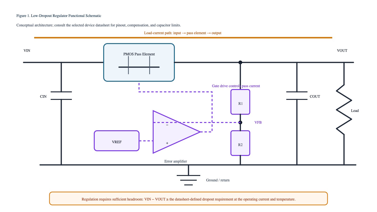
Figure 1. Conceptual LDO architecture and control loop. Datasheet-specific pinout, compensation, and capacitor limits still apply.
Dropout voltage is the input-to-output differential at which the regulator can no longer meet its output specification. Datasheets define it under stated load and temperature conditions. It generally increases with load because the pass path has finite resistance. Budget minimum battery voltage, path loss, output tolerance, temperature, and worst-case dropout rather than relying on a typical value.
PSRR describes how much AC input disturbance reaches the output; output noise is generated inside the regulator. PSRR varies with frequency, load, headroom, capacitance, and architecture. Reduced headroom can sharply degrade it before or near dropout. A 1 kHz figure does not establish rejection at a 2 MHz switching frequency.
Quiescent current powers the regulator's internal circuitry and matters most at light load or in sleep. Because ground-current and quiescent-current terminology varies, use the datasheet's definitions and mode tables.
For a first estimate with negligible quiescent current,
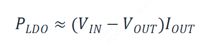
and
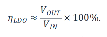
A more complete power balance is

provided Iq represents input current that does not reach the load. At 5 V to 3.3 V and 300 mA, the simplified loss is 0.51 W and the idealized efficiency is 66%. At 12 V to 3.3 V and 1 A, the loss is 8.7 W and the idealized efficiency is 27.5%.
The package, copper, vias, stack-up, airflow, and enclosure turn electrical loss into junction-temperature rise. Thermal resistance is credible only when the real assembly resembles the test board; board construction can change the result substantially.
How a Switching Regulator Works
A synchronous buck alternates high-side and low-side MOSFET conduction. The inductor limits current slew, the output capacitor handles the difference between inductor and load current, and the controller adjusts timing to regulate the output. A nonsynchronous buck uses a diode for the low-side path. Boost and buck-boost topologies have different critical current paths.
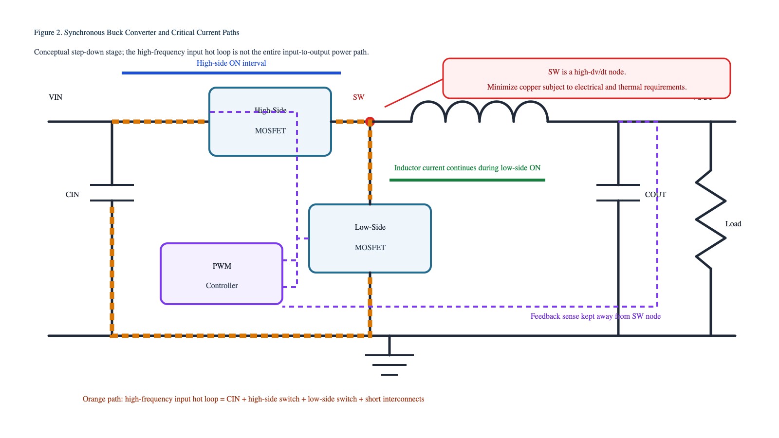
Figure 2. Conceptual synchronous buck stage. The highlighted hot loop comprises CIN, the switching FETs, and their short interconnects.
The buck avoids continuous pass-element loss but is not lossless. MOSFET conduction and switching, gate drive, controller current, magnetics, and capacitor ESR all contribute. Efficiency changes with voltage, load, frequency, mode, temperature, and components.
For the 12 V to 3.3 V, 1 A example, assume a representative efficiency of 90%:
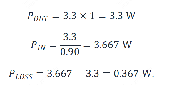
The loss is not
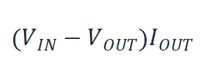 that expression models a linear regulator.
A buck's output ripple is periodic residue related to ripple current, capacitance, ESR, mode, and layout. Switching transients are higher-frequency ringing and spikes. Neither is the same as radiated EMI. Long probe ground leads can exaggerate apparent spikes, so measurements need a stated method and bandwidth.
Inductance affects ripple and transient current slew. DCR produces copper loss; material and frequency affect core loss; saturation can reduce inductance and drive a steep current rise. Check peak current, RMS heating, tolerance, temperature derating, shielding, and faults.
LDO vs Switching Regulator: Key Differences
"LDOs are quiet and switchers are efficient" is too crude. An LDO can lose PSRR near dropout; a low-ripple switcher can still couple harmonics into a cable. The useful comparison is conditional.
Efficiency, Power Loss, and Thermal Feasibility
At 5 V to 3.3 V and 300 mA, an LDO delivers 0.99 W and loses 0.51 W. That may be acceptable in a thermally enhanced implementation yet excessive in a small package with little copper at high ambient temperature.
At 12 V to 3.3 V and 1 A, the LDO loses 8.7 W. The example buck loses 0.367 W only under the 90% assumption. Use the selected converter's data across voltage, load, temperature, and mode, including inductor loss.
Rules such as "switch above 1 W," "use an LDO below 300 mA," or "buck above 2:1" are prompts, not physical limits. Thermal viability depends on the package, PCB, airflow, ambient temperature, duty cycle, and junction limit.
Noise, PSRR, Ripple, and EMI
Intrinsic noise originates inside the regulator. PSRR attenuates an input disturbance. Ripple is periodic output variation. Conducted and radiated EMI describe energy coupling. One "quietness" number hides these different mechanisms.
An LDO can suit a sensitive rail if its integrated noise and PSRR match the relevant band. PSRR can collapse near dropout. A modern buck can also achieve low ripple through device choice, mode, filtering, and layout. Low load-point ripple does not guarantee low radiated emissions because the switch node can couple into traces, shields, and cables.
Footprint, Cost, and Transient Response
Compare complete implementations, not package outlines. An LDO may need thermal copper or a heatsink. A buck adds magnetics and passives, but modules can be compact. Height, filters, keepouts, and test access also count.
Neither class has a universal transient advantage. The local capacitor handles the initial current difference; ESR, ESL, capacitance, and interconnect set the immediate excursion. Loop and power-stage dynamics govern recovery. Smaller buck inductance can increase current slew but also raises ripple and peak current. Compare identical load steps, edge rates, capacitance, deviation limits, and recovery definitions.
| Design Factor | LDO | Synchronous Buck Regulator |
|---|---|---|
| Efficiency | Approaches $V_{out}/V_{in}$ when quiescent current is negligible | Depends on operating point, mode, IC, inductor, capacitors, and frequency |
| Main loss mechanism | Voltage drop across the pass path, plus internal current | MOSFET, gate-drive, control, inductor, and capacitor losses |
| Thermal behavior | Loss rises directly with voltage drop and load current | Often lower for a large step-down ratio, but the IC and inductor can create local hot spots |
| Output noise | Can be very low in a purpose-built device | Includes switching-related spectral content; low-noise converters exist |
| PSRR | Explicit, frequency-dependent input-ripple rejection | Usually described through line response, loop behavior, and output filtering rather than an LDO-style PSRR figure |
| Output ripple | Does not generate a switching fundamental, but input ripple passes according to PSRR | Depends on ripple current, capacitance, ESR, mode, layout, and measurement bandwidth |
| EMI | No internal power-switch hot loop | High-di/dt and high-dv/dt nodes can create conducted and radiated emissions |
| Components | Often the IC and input/output capacitors; adjustable parts add a divider | IC, inductor, input/output capacitors, divider, and sometimes bootstrap, compensation, snubber, or filter parts |
| PCB area | Often small at low dissipation; thermal copper may dominate at higher loss | May be compact, especially as a module, but magnetics, height, filtering, and keepouts count |
| Low-load operation | $I_q$ may dominate input current | PFM or pulse skipping can save power but changes ripple and spectral behavior; forced PWM has different trade-offs |
| Transient response | Depends on loop, headroom, local capacitance, ESR/ESL, and load edge | Depends on control law, compensation, inductance, capacitance, mode, and operating point |
| Design effort | Lower in many applications, but stability and heat still need verification | Higher because power-stage selection, switching layout, thermal behavior, and EMI interact |
Combining an LDO and Switching Regulator
Many systems use this power chain:
buck converter → LDO → sensitive load
The buck handles the large conversion. The LDO attenuates some conducted disturbance within its PSRR limits. This is not galvanic isolation; high-frequency coupling can bypass the LDO.
The minimum buck output, including ripple and transient dip, must preserve LDO dropout and tolerance margin. Extra headroom becomes heat. For a 5 V buck feeding a 3.3 V LDO at 100 mA, the LDO loses 0.17 W. At an assumed 90% buck efficiency, buck loss is about 0.056 W and end-to-end efficiency is 59.4%. The chain may still make sense if 5 V already exists or its noise benefit is justified.
An intermediate rail near the final voltage reduces loss. For example, 3.6 V might support one 3.3 V LDO only after tolerance, droop, dropout, load, and temperature are checked; it is not a universal recommendation.
Startup is system-specific. Check enable thresholds, soft start, discharge, prebias, sequencing, and reverse current instead of assuming that the buck must simply start first.
Integrated PMICs show how common mixed regulation is. The ADP5037 combines two 800 mA buck regulators and two 300 mA LDOs in a 4 mm × 4 mm package, but its supply range does not permit direct operation from 12 V. The TPS65023 family combines three step-down converters and three LDO functions for systems powered from one Li-ion or Li-polymer cell. These are architecture examples, not interchangeable solutions for the 12 V case.
PCB Layout Guidelines
PCB parasitics complete the real power circuit. A correct schematic can still oscillate, run hot, corrupt feedback, or fail emissions.
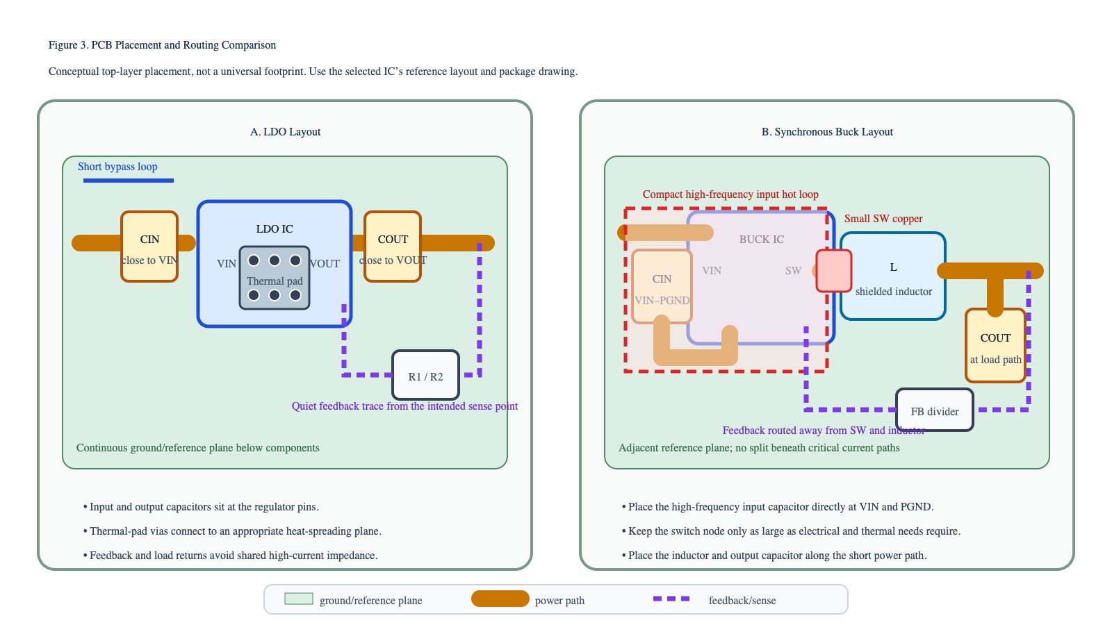
Figure 3. Conceptual placement comparison. Follow the selected IC's reference layout and package instructions.
LDO Layout Best Practices
Keep the input-bypass loop short and low impedance. Place the required output capacitor and return according to the reference layout. Shared paths can reduce bypass effectiveness or couple load current into the regulator ground.
Some older or specially compensated LDOs need a defined ESR range. Ceramic-stable architectures permit very low ESR but may still bound capacitance or ESR. Follow the part's stability requirements across load and temperature. X5R or X7R MLCCs can lose capacitance under DC bias.
For an adjustable LDO, route feedback from the intended sense point, away from noisy or high-current conductors. Keep load-return impedance out of the sense ground. Follow the selected datasheet's exposed-pad connection, land, paste, and via instructions; the pad is not automatically ground.
Copper spreads heat into the board; thermal vias may connect an exposed pad to other planes. No universal three-to-five-via or 0.5 W rule survives differences in via geometry, planes, stack-up, airflow, and assembly. Model the board and test the assembled LDO layout at worst case.
Switching Regulator Layout Best Practices
For an integrated synchronous buck, the hot loop is primarily the high-frequency input capacitor and switch cell. It is the difference between on- and off-state current paths, not the entire input-to-output power path.
Place the high-frequency input ceramic capacitor directly across VIN and power ground with a short, low-inductance connection. This limits ringing and magnetic radiation from the high-di/dt path.
The high-dv/dt switch node presents a different problem, as addressed in TI's LMR60406-Q1 layout guidelines: keep its copper no larger than current, thermal, and manufacturing needs require.
An adjacent reference plane helps contain returns. Do not split it so current must detour. Some datasheets call for a switch-node keepout to reduce parasitic capacitance, so "solid ground everywhere" is not universal.
Wider current paths reduce conduction loss, but a large switch node may worsen coupling. Follow package thermal guidance without enlarging noisy copper. ADI reported about a 20 dB emissions difference between specific LT8614 and LT8610 demonstration boards. That does not support universal 10–20 dB EMI or 1–3% efficiency claims.
CISPR 25 concerns disturbances that can affect receivers in vehicles and related equipment; its test configuration belongs in the product EMC plan. FCC Part 15 Subpart B covers specified unintentional radiators, including covered digital devices and external switching supplies. Neither is a PCB-layout standard or applies merely because a board contains a buck converter.
For a more detailed checklist, see JLCPCB's guide to switching regulator PCB layout best practices.
How to Choose an LDO or Switching Regulator
- Define the complete input range. Include battery state, adapter tolerance, surge requirements, upstream voltage drop, and startup behavior.
- Set the output limits. Combine DC accuracy, line and load regulation, ripple, transient deviation, interconnect drop, and remote-sense error where applicable.
- Build the load profile. Record typical, maximum, peak, standby, and reverse-current conditions. Define load-step amplitude and edge rate.
- Calculate LDO loss. Use the highest relevant input voltage and load current. Include quiescent or ground-current terms when they materially affect input power.
- Test thermal feasibility on paper. Check package, board copper, stack-up, vias, airflow, ambient limit, neighboring heat sources, and maximum junction temperature.
- Check dropout headroom. Use worst-case dropout at the required current and temperature, not the headline typical value.
- Set an efficiency or battery-life target. For the buck option, inspect efficiency across the actual input, load, mode, and temperature range. For the LDO, include $I_q$ at light load.
- Define noise and EMI requirements. Identify sensitive frequency bands, allowable ripple, cable-coupling paths, and applicable conducted or radiated tests.
- Specify transient behavior. State the load step, edge rate, local capacitance, maximum deviation, and recovery criterion.
- Compare total implementation area. Include magnetics, filter parts, thermal copper, component height, keepouts, and test access.
- Compare complete cost. Count design time, EMI debugging, thermal hardware, battery capacity, and enclosure impact as well as BOM price.
- Evaluate a hybrid rail. Add an LDO after a buck only when measured or datasheet-backed noise rejection justifies the extra loss and complexity.
The common search phrase LDO vs buck regulator does not resolve to one current or voltage-ratio threshold. A 50 mA LDO can overheat with enough voltage drop, while a 1 A LDO can be practical with low headroom and adequate cooling.
| An LDO Is a Strong Candidate When… | A Buck Regulator Is a Strong Candidate When… | |
|---|---|---|
| Thermal | Worst-case dissipation and junction temperature are acceptable | Linear loss would be thermally or energetically unacceptable |
| Headroom | Input headroom remains adequate across all conditions | A large voltage reduction or higher output power is required |
| Noise | A specific LDO meets noise and PSRR requirements in the relevant band | Efficiency or battery runtime is a primary constraint |
| Simplicity | Simplicity or low component count matters more than the conversion loss | The design can support magnetics, switching layout, and EMC validation |
| Post-regulation | The rail needs justified post-regulation after a switcher | Low-load mode behavior is compatible with the load's noise requirements |
Common Design Mistakes
Mistakes to Avoid
- Selecting an LDO from voltage and current ratings alone. The device may meet both ratings and still overheat. Calculate worst-case dissipation, estimate junction temperature with a board-relevant thermal model, and test the assembly.
- Budgeting only typical dropout. Minimum battery voltage, path resistance, output tolerance, load, and temperature can force the regulator out of regulation. Build a worst-case headroom budget from guaranteed data.
- Putting the buck input capacitor near the connector instead of the switch cell. The bulk input capacitor may be close to the connector, but the high-frequency ceramic capacitor belongs at VIN and power ground. Extra loop inductance increases ringing and emissions. Use the reference layout rather than a universal distance such as 5 mm.
- Treating the whole buck power path as the hot loop. This sends layout effort to the wrong geometry. Identify the topology's fully switched current loop, then minimize the relevant loop area and parasitic inductance.
- Making switch-node copper unnecessarily large. More area increases capacitive coupling from the high-dv/dt node. Use enough copper for the electrical and thermal requirement, then protect feedback and other sensitive routes.
- Assuming every LDO accepts the same output capacitor. A ceramic capacitor that stabilizes one architecture may destabilize another. Verify capacitance, ESR, load range, temperature, and DC-bias derating in the exact datasheet.
- Ignoring inductor saturation and temperature rise. Falling inductance raises ripple and peak current; DCR and core loss raise temperature. Check peak and RMS current at temperature as well as nominal inductance.
- Treating a typical efficiency curve as guaranteed performance. It represents one test configuration and selected conditions. Measure the complete power stage at the product's voltage, load, mode, and temperature corners.
FAQ about LDO vs Switching Regulator
Q: Is an LDO Better Than a Switching Regulator?
Neither is universally better. An LDO can be the simpler choice when headroom and current produce acceptable loss and a specific device meets the noise requirement. A switcher is often favored when linear dissipation or battery-energy loss would be excessive.
Q: When Should I Use an LDO Instead of a Buck Converter?
Use an LDO when worst-case dropout, junction temperature, efficiency, stability, and noise performance all fit the system. Small voltage differences, modest loads, always-on rails with carefully selected $I_q$, and post-regulation are common cases, not hard rules.
Q: Can I Use an LDO After a Switching Regulator?
Yes. Check minimum headroom during ripple and transients, PSRR at the switching frequency and harmonics, LDO dissipation, startup sequencing, prebias, output discharge, and reverse-current paths.
Q: Why Are LDO Regulators Often Quieter?
An LDO has no internal switch node or inductor hot loop, so it does not create that class of periodic switching disturbance. It still generates intrinsic noise and passes input disturbances according to its frequency-dependent PSRR. A carefully designed low-noise switcher can outperform an unsuitable LDO in a particular frequency band.
Q: How Do I Calculate LDO Power Dissipation?
With negligible quiescent current, use $P_{loss} = (V_{in} - V_{out}) \times I_{out}$. If internal current matters, use an input-output power balance based on the datasheet's current definitions. Evaluate the highest relevant input, load, and ambient conditions, then translate the result into junction temperature using a model appropriate to the package and PCB.
Conclusion: LDO vs Switching Regulator
Choose the regulator from the operating envelope, not from a slogan. An LDO is attractive when its voltage drop, current, headroom, stability, noise, and thermal limits fit the rail. A buck converter makes larger step-down ratios and higher-power conversion practical, but it introduces magnetics, switching losses, fast current loops, switch-node coupling, and EMC work. Hybrid regulation is useful when the LDO's measured or specified post-regulation benefit justifies its added headroom and heat.
Reserve the power-stage area, copper, planes, thermal paths, and test points early. Then validate efficiency, temperature, ripple, load transients, and emissions on assembled hardware under defined operating corners.
For engineers who need help taking a reviewed power schematic through PCB implementation, JLCPCB offers a PCB Layout Service. Supply the regulator datasheets, stack-up, current paths, thermal constraints, placement restrictions, and applicable EMC requirements so the layout can be reviewed against the actual design conditions before fabrication.
Keep Learning
Track Width v/s Current Capacity: PCB Layout Tips for Power Routing
Key Takeaways Trace width and copper thickness set the current limit. Standard 1 oz (35 µm) copper suits most designs; step up to 2–3 oz for power-hungry boards. Size traces against IPC-2221/IPC-2152 for a safe temperature rise. Internal layers carry less current than external ones. Buried traces dissipate heat poorly, so derate them or move high-current paths to outer layers. Vias are a bottleneck—each carries only about 500 mA. When routing power across layers, stitch multiple vias in parallel rathe......
Circuit Board Ground Plane and Power Plane Guide 2026
Key Takeaways Continuous copper first: A solid circuit board ground plane creates a low-impedance return path, reduces noise, and is usually safer than split planes, even on mixed-signal boards. Think in current loops: Every signal needs a return path directly beneath it. Never route high-speed traces across plane gaps, slots, or cutouts. Plan the stack-up early: Choose the layer arrangement before routing critical signals, and keep power and ground planes close together to lower distribution inductan......
Guide to Ground Bounce in PCB - Causes, Effects & Prevention
Key Takeaways Ground bounce is a voltage spike between an IC's die ground and the PCB ground. It happens when current changes fast through parasitic inductance (V = L x di/dt). Many outputs switching at once, called SSO, make it much worse. It can cause logic errors, false resets, and ringing on signals. You measure it with a quiet-low sense line on a scope. Good decoupling, short ground loops, and slower slew rates fix most of it. Introduction A board passes every test on the bench. Then, in the fiel......
Voltage Regulator PCB: Practical Design Guide
Key Takeaways A voltage regulator PCB doesn't just convert one voltage into another; it must also provide a stable output while handling heat, load changes, and noise in the circuit. The layout is as important as the regulator IC; keep the input and output capacitors near the pins, use short power connections, and ensure a direct, low-impedance ground return. Linear regulators are simple and quiet, but they lose voltage difference as heat; switching regulators are the better option when the voltage dr......
LDO vs Switching Regulator: Comparison & PCB Layout
Key Takeaways Calculate LDO dissipation first: Always calculate LDO power dissipation at maximum input voltage and load before comparing packages or prices. Condition-dependent specs: Treat dropout, PSRR, noise, ripple, efficiency, and transient response as condition-dependent, not fixed values. Layout matters for both: A buck converter's high-di/dt input loop and high-dv/dt switch node create different coupling mechanisms. Both need deliberate PCB placement. Output capacitor selection: The output cap......
Understanding Star Grounding in PCB Design: A Practical Guide
Key Takeaways Controlled Return Paths: Star grounding gives selected circuit blocks separate return paths that meet at one controlled physical point. It limits shared-impedance coupling between noisy and sensitive sections. Best Applications: It works best in compact, low-frequency, low-current, or noise-sensitive systems, including audio stages, sensor interfaces, and selected precision circuits. Ground Plane Alternative: A ground plane provides a broad, low-inductance reference that is normally bett......