
Backdrill Vias: Enhancing Signal Integrity in High-Speed PCBs
10 min
- The Growing Demand for  High-Speed PCBs
- Understanding Backdrill Via: Definition and Mechanism
- Key Benefits of Implementing Backdrill Vias
- The Backdrilling Process: From Design to Fabrication
- Comparing Backdrill Vias with Alternative Solutions
- JLCPCB's Expertise in Backdrill Via Manufacturing
- FAQ for Backdrill Vias
- Conclusion
Key Takeaways
Backdrill vias remove unused copper stubs from plated through-hole vias, shortening the residual stub to under 0.15 mm (6 mils). This eliminates impedance discontinuities, reflections, and resonances in high-speed signals above 5–10 Gbps. It delivers better return loss, insertion loss, lower jitter, and clearer eye diagrams — all while keeping simple stack-ups and far lower cost than blind/buried vias. Use backdrilling for any stub longer than 15 mils (0.381 mm), especially on boards thicker than 1.2 mm, to ensure reliable performance in PCIe, 5G, and 25G+ designs.
In high-speed PCB designs running at 10 Gbps and beyond, via stubs create impedance discontinuities that degrade signals through reflections and resonances. Backdrill vias solve this by mechanically removing the unused copper barrel after initial plating, leaving only the functional electrical path. This manufacturing step restores transmission-line continuity without changing layer stack-up or trace geometry. Engineers specify backdrill vias in fabrication notes to achieve cleaner eye diagrams, lower jitter, and reliable performance in multilayer boards for 5G, PCIe, and SerDes applications.
The Growing Demand for High-Speed PCBs
Challenges in Signal Transmission
High-speed signals above 5 GHz treat a plated through-hole via as a short transmission line segment. When the via connects only inner layers, the unused portion—known as the stub—behaves like an open-circuited stub with characteristic impedance around 50–70 Ω depending on dielectric constant and geometry. This stub introduces parasitic capacitance of roughly 0.5–1 pF per mm of length and inductance of 0.3–0.5 nH per mm, forming a resonant structure.
The quarter-wavelength resonance frequency can be approximated as:
f = c / (4 × L_stub × √ε_r)
where c is the speed of light, L_stub is the stub length in meters, and ε_r is the relative permittivity (typically 4.0–4.5 for FR-4). For a 0.5 mm stub on standard FR-4, resonance appears near 10–12 GHz, exactly in the Nyquist band of many 25 Gbps channels.
The result is a sharp notch in the insertion-loss (S21) curve and a peak in return loss (S11), often exceeding –10 dB return loss at the resonant frequency. In differential pairs , even a 0.1 mm length mismatch between P and N stubs adds skew of 0.5–1 ps, violating tight timing budgets in DDR5 or 100G Ethernet. Crosstalk also rises because the stub radiates energy into adjacent vias and planes. Without mitigation, designers must add pre-emphasis, equalization, or limit channel length—none of which address the root cause. JLCPCB’s high-speed design guidelines explicitly identify via stubs longer than 15 mils (0.381 mm) as requiring backdrilling to prevent these effects, aligning with industry practice for boards thicker than 1.0 mm.
Understanding Backdrill Via: Definition and Mechanism
What is a Backdrill Via?
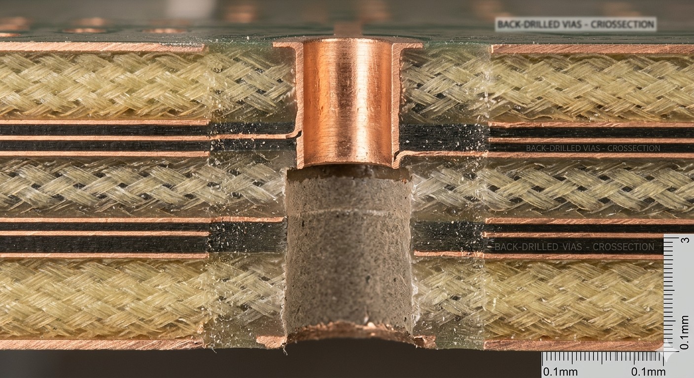
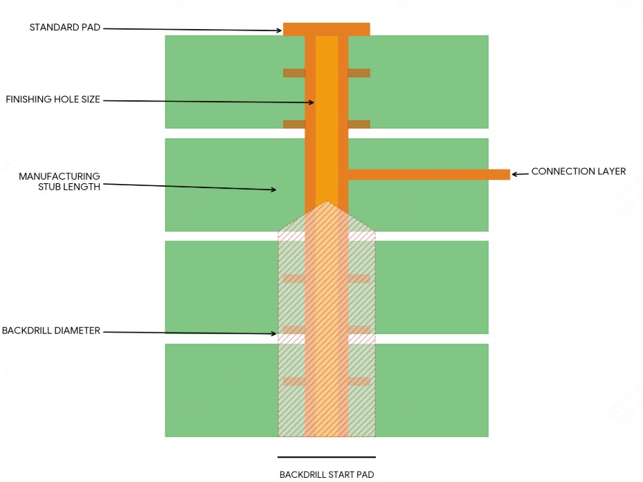
A backdrill via starts as a standard plated through-hole (PTH) via drilled and electroplated during the primary fabrication sequence. After outer-layer etching, a secondary controlled-depth drill from the opposite side of the board removes the copper barrel beyond the last connected signal layer. The backdrill bit diameter is typically 0.1–0.25 mm larger than the original via drill to guarantee complete copper removal without sidewall damage. The finished stub length is held to under 0.15 mm (approximately 6 mils), turning the via into an electrically short interconnect that matches the impedance of the connecting traces. This process does not affect the mechanical integrity of the board when performed within JLCPCB’s documented depth tolerance of ±0.1 mm.
How Backdrilling Removes Via Stubs
The backdrilling sequence occurs after plating and before solder mask application. CNC machines with laser depth sensors and vision alignment locate the exact start pad on the back side. The drill penetrates the unused layers, excising the barrel while leaving the functional copper intact on the target layer. Debris is evacuated with vacuum and ultrasonic cleaning to prevent plating voids or shorts. The larger backdrill diameter creates a slight annular clearance on unused planes, which is pre-accounted for in DFM by enlarging antipads on those layers by 0.1 mm. JLCPCB’s process supports backdrilling on 4- to 32-layer boards, ensuring the residual stub remains below the 15-mil threshold that triggers resonance.
Cross-section analysis of test coupons confirms removal: the original barrel ends cleanly at the target layer with no hanging copper. Electrical validation via time-domain reflectometry (TDR) shows the impedance discontinuity dropping from >20 % to <5 % after backdrilling. This step adds minimal cost—typically 5–10 % for high-layer boards—while delivering performance equivalent to more expensive blind or buried vias for most signal nets.
Key Benefits of Implementing Backdrill Vias
Improved Signal Integrity
Backdrill vias eliminate the dominant source of via-induced reflection coefficient (Γ). In full-wave 3D EM simulations, a 0.5 mm stub produces Γ ≈ 0.3–0.4 at 10 GHz; backdrilling reduces this to Γ < 0.05 across the entire bandwidth. The eye diagram opens by 30–50 %, with deterministic jitter falling below 5 ps for 25 Gbps channels. Differential impedance remains uniform because the via no longer presents excess capacitance on one leg. Return paths through reference planes stay continuous, minimizing common-mode conversion and EMI radiation from the via site.
Reduced Insertion Loss and Reflections
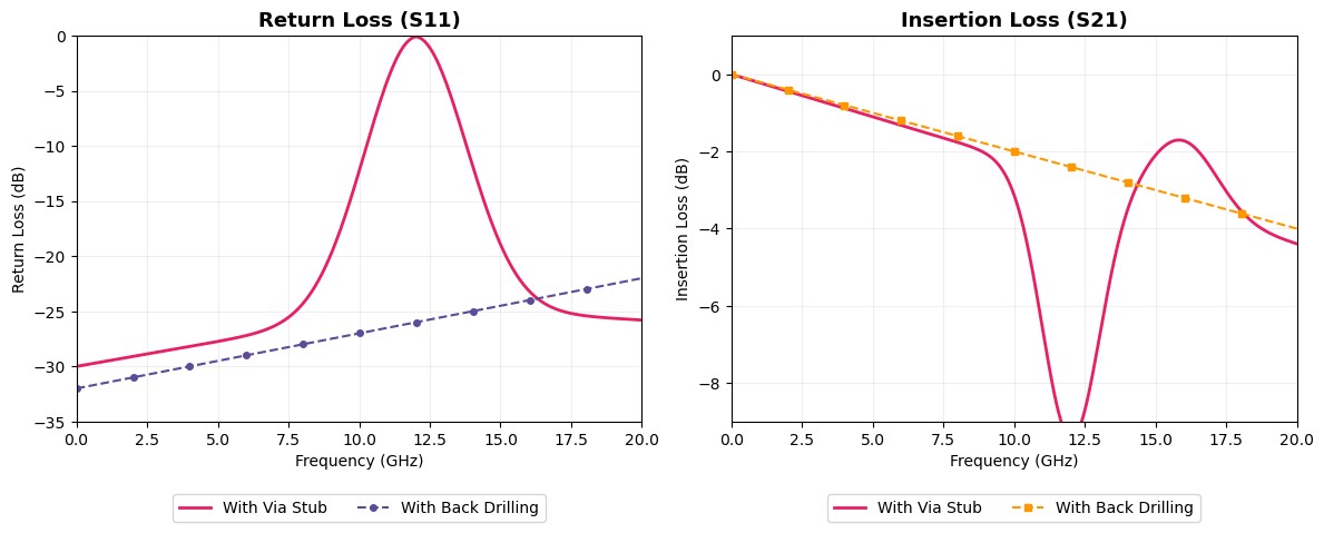
Insertion loss improves by 1–3 dB across 5–20 GHz because the stub resonance is removed. Return loss flattens, with S11 staying below –20 dB up to the Nyquist frequency instead of spiking to –8 dB. Group delay variation drops below 10 ps, critical for phase-sensitive applications like 5G beamforming. The table below quantifies gains on a typical 10-layer, 1.6 mm thick board with 0.2 mm vias.
Table 1: Performance Comparison – Via Stub vs. Backdrilled Via (10 Gbps differential pair, 10-layer board)
| Metric | With 0.5 mm Stub | Backdrilled (<0.15 mm Stub) | Improvement |
|---|---|---|---|
| Return Loss @ 5 GHz | –12 dB | –22 dB | +10 dB |
| Insertion Loss @ 5 GHz | –3.5 dB | –1.8 dB | 1.7 dB better |
| Peak-to-Peak Jitter | 18 ps | 9 ps | 50 % reduction |
| Eye Height (UI) | 0.55 | 0.78 | +42 % |
| Resonance Frequency | ~11 GHz | None in band | Eliminated |
Enhanced Performance in High-Frequency Applications
In mmWave front-ends and phased-array antennas, backdrill vias cut radiation loss and coupling between adjacent vias by 6–8 dB. At 28 GHz and above, the stub acts as a monopole antenna; removing it prevents energy leakage into the cavity formed by power/ground planes. For JESD204C serial links or 112 Gbps PAM4 channels, backdrilling enables longer trace runs without additional SerDes equalization, reducing power consumption by 15–20 % at the receiver.
The Backdrilling Process: From Design to Fabrication
Design Considerations for Backdrill Vias
Specify backdrill requirements in Gerber/ODB++ files using layer callouts or fabrication notes: target layer, backdrill diameter (original drill +0.1 mm minimum), and maximum residual stub length. Antipads on unused layers must be enlarged by 0.1 mm to provide clearance for the larger backdrill bit. Avoid via-in-pad unless backdrilling is explicitly confirmed feasible, as solder wicking into the backdrilled hole can occur. Simulate the full channel—including trace, via, and backdrilled segment—with 3D solvers to verify S-parameters before tape-out. JLCPCB recommends flagging any via whose functional length exceeds 15 mils for backdrilling to maintain consistent impedance.
Advanced Backdrilling Equipment and Techniques
JLCPCB employs high-RPM (up to 150,000) CNC drills with closed-loop servo control and laser interferometry for depth accuracy of ±0.05 mm. The process runs after outer-layer etching but before solder mask, using vision systems to align to fiducials within 10 µm. Drill bits are carbide with specialized geometries to minimize burrs; vacuum extraction and high-pressure air purge remove debris instantly. For dense panels, multiple depth settings are programmed per board to handle varying layer counts in one pass.
Quality Control and Precision Assurance
Every production panel includes test coupons with representative backdrilled vias. Cross-sectioning verifies stub length <0.15 mm and no residual copper. Automated optical inspection (AOI) scans for exposed barrel edges, while TDR and vector network analyzer (VNA) testing on flying probes confirms impedance continuity. JLCPCB’s ISO-certified process tracks depth tolerance across the entire panel, rejecting any via outside specification before shipping. This level of in-house control ensures repeatable results across prototype and volume runs.
Comparing Backdrill Vias with Alternative Solutions
Backdrill Via vs. Blind and Buried Vias
Blind and buried vias eliminate stubs by design but require sequential lamination, additional laser drilling, and higher layer counts—raising cost by 30–100 % and extending lead time. Backdrill vias use the same initial PTH process as standard multilayer boards, keeping stack-up simple and economical. Electrical performance is nearly identical for signals below 30 GHz because the residual stub is electrically short. A hybrid strategy—backdrill for long runs and microvias for BGA fan-out—often delivers the best density and cost trade-off.
When to Choose Backdrilling for Your Project
Apply backdrilling when data rates exceed 5 Gbps and board thickness forces stub lengths >15 mils, or when differential skew budgets are tighter than 5 ps. It is the preferred choice for boards 1.2 mm and thicker where blind vias would force HDI stack-ups. Budget-conscious projects benefit because backdrilling adds far less cost than extra lamination cycles. Always verify manufacturability with the fabricator’s DFM report before finalizing layout.
JLCPCB's Expertise in Backdrill Via Manufacturing
Our Advanced Capabilities and Services
JLCPCB integrates backdrilling into its standard multilayer workflow for 4–32 layers, using precision CNC equipment calibrated daily for depth repeatability. Real-time DFM checks flag vias needing backdrilling based on the 15-mil stub rule, and controlled-impedance options are fully compatible. Engineers receive detailed fabrication notes confirming exact backdrill depths and clearances.
Case Studies: Successful Projects with JLCPCB Backdrill Vias
A 12-layer 25 Gbps networking board achieved 40 % eye-height improvement and passed PCIe 5.0 compliance after backdrilling 48 critical differential vias. An mmWave 5G module reduced return-loss notches by 8 dB, eliminating the need for external equalizers and cutting BOM cost by 12 %. Both projects used JLCPCB’s standard FR-4 process with backdrilling, demonstrating repeatable results without stack-up changes.
Why Partner with JLCPCB for Your High-Speed PCB Needs
JLCPCB combines in-house drilling expertise, online impedance calculators, and instant DFM feedback that catches stub issues before production. Their documented guidelines and high-volume experience ensure every backdrilled via meets tight tolerances, giving designers confidence from prototype to mass production.
FAQ for Backdrill Vias
Q1: What is a backdrill via?
A backdrill via is a plated through-hole via where the unused copper stub is mechanically drilled out from the opposite side of the board after fabrication, leaving a very short residual stub (typically <0.15 mm).
Q2: Why is backdrilling important for high-speed PCBs?
It removes via stubs that cause reflections, resonance, and signal degradation above 5 GHz, significantly improving return loss, insertion loss, and eye diagram quality.
Q3: What is the maximum recommended stub length before backdrilling?
JLCPCB recommends backdrilling any via stub longer than 15 mils (0.381 mm) to avoid resonance issues in high-speed designs.
Q4: How much does backdrilling add to PCB cost?
Backdrilling typically increases cost by 5–10% depending on layer count and quantity. It is far more economical than switching to blind or buried vias.
Q5: Can backdrilling achieve the same performance as blind vias?
For most applications below 30 GHz, backdrill vias deliver near-equivalent electrical performance while keeping the stack-up simpler and lower cost.
Conclusion
Backdrill vias deliver measurable signal-integrity gains through precise stub removal, enabling reliable high-speed performance without complex redesigns. By following JLCPCB’s guidelines—keeping stubs under 15 mils and applying backdrilling where needed—designers achieve lower reflections, flatter loss profiles, and higher margins in demanding applications.
Keep Learning
Effective Escape Routing Strategies for High-Density BGA Success
Key Takeaways Escape routing is essential for successfully fanning out high-density BGAs, especially at 0.5 mm pitch and below. Use dogbone fanout for ≥0.5 mm; switch to via-in-pad (filled & capped) for finer pitches. HDI microvias and stacked vias significantly improve routing density and reduce layer count. Maintain symmetry and short stubs for differential pairs to preserve signal integrity. Combine smart stackup, DFM checks, and capable fabrication for reliable, high-yield results. Ever put a 484-......
Building Reliable High-Speed Performance with Effective Timing Analysis
Key Takeaways Timing analysis is essential for high-speed PCBs — clean signals can still fail if they miss setup or hold windows. Focus on setup time, hold time, clock skew, and propagation delay to ensure reliable data sampling. Prioritize length matching, controlled impedance, and proper stackup to maintain positive timing margins. Combine static timing analysis with dynamic simulation for best results. Precision manufacturing is critical — small variations in impedance or dielectric thickness can d......
Low Loss PCBs : Advanced Materials for Superior High-Speed Signal Performance
Key Takeaways Low Loss PCBs using advanced materials like Rogers RO4003C, RO4350B, and PTFE laminates deliver superior signal integrity by dramatically reducing dielectric loss at multi-gigahertz frequencies. Ideal for 5G, mmWave, RF, and high-speed digital designs, these boards offer significantly lower insertion loss, stable impedance, and better thermal performance compared to standard FR4. By choosing the right low-loss laminate and partnering with experienced manufacturers like JLCPCB, engineers ......
How to Reduce Insertion Loss for Better High-Speed PCB Performance
Key Takeaways Reducing insertion loss is essential for achieving reliable high-speed PCB performance. By selecting low-loss materials with lower Df, optimizing trace routing and stackup design, minimizing via transitions, using smoother copper foils, and applying precision manufacturing techniques, designers can significantly lower both dielectric and conductor losses. These strategies help maintain better signal integrity, wider eye openings, and higher data rates in multi-gigabit designs. Have you e......
How to Create the Perfect PCB Stackup for High-Speed and Reliable Designs
Key Takeaways A well-designed PCB stackup is the foundation of high-speed, reliable designs, determining signal integrity, controlled impedance, and EMI performance. Use symmetrical layers with adjacent reference planes, proper dielectric spacing, and copper balancing to avoid warpage and crosstalk. Choose standard FR4 for <3 GHz or low-loss materials (Megtron 6, Rogers) for higher speeds, and work closely with manufacturers for optimal results. Mastering your stackup is essential for high-speed succe......
Achieving Reliable High-Speed Performance with PCB Transmission Lines
Key Takeaways PCB Transmission Lines are essential for reliable high-speed PCB performance in USB 3.0, PCIe, DDR4, and RF designs, turning traces into controlled-impedance structures that eliminate reflections, crosstalk, and attenuation. Select microstrip, stripline, or GCPW geometries with accurate calculations, continuous reference planes, mitered bends, and 3W spacing, then rely on precise etching, copper profile control, and TDR testing at JLCPCB for consistent results from prototype to volume pr......