
The Benefits of High Speed PCBs : Advanced Design and Manufacturing for Reliable Data Rates
12 min
- Advanced Materials Essential for High Speed Performance
- Proven Design Approaches for Reliable High Speed PCBs
- Precision Manufacturing for Flawless High Speed PCBs
- JLCPCB’s Specialized Capabilities in High-Speed PCB Production
- Frequently Asked Questions (FAQ)
What is high-speed PCB design, then? It is not just the frequency cut-in, High-speed. When the characteristics of the traces become unfriendly to the signal, trace impedance, via parasitic, material losses, signal coupling, etc., really begin to affect the signal quality, and you can no longer simply plug it in and hope for the best, it must be designed.
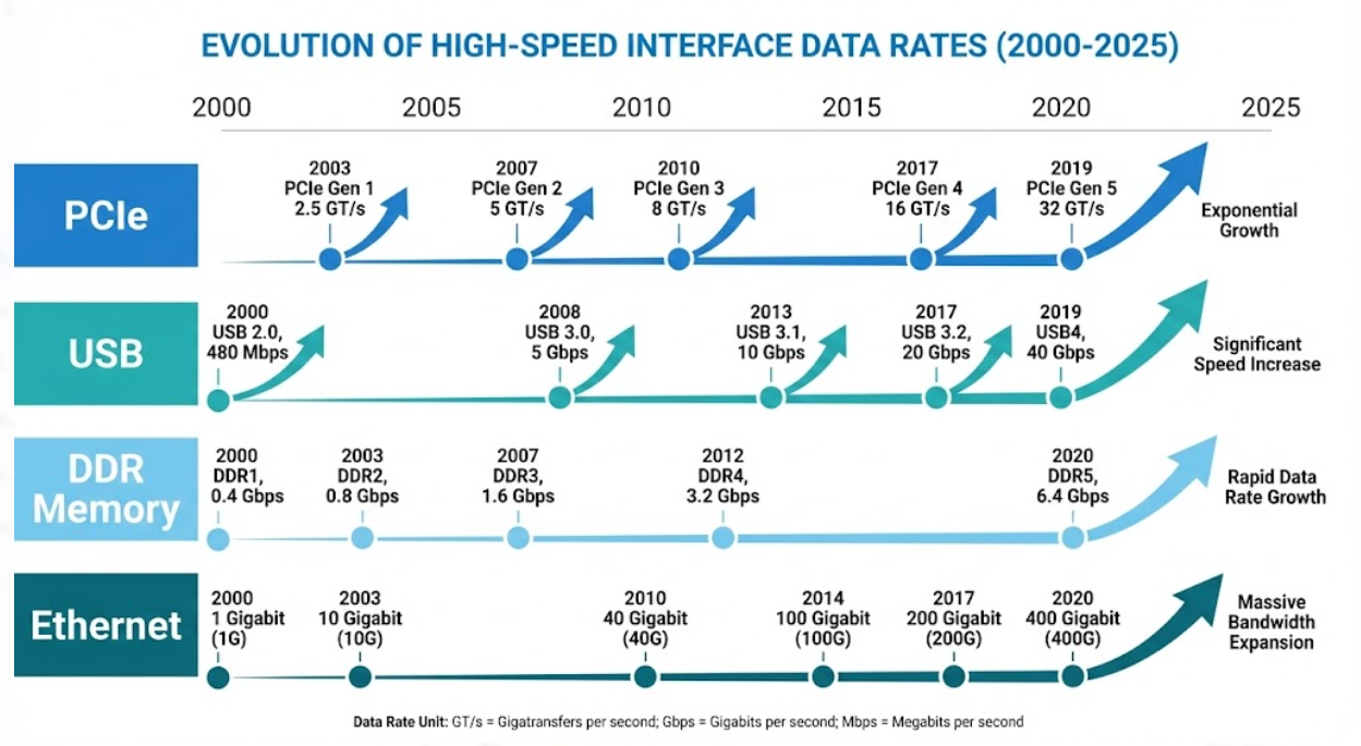
Practically, that typically implies rise times in the range of nanoseconds, data rates in the range of gigabit per lane, or clock speeds in the range of several hundred megahertz. However, modern interfaces are far beyond those limits: PCIe Gen5 can run at 32GT/s, USB4 at 40GB/s, DDR5 at 6.4GB/s, and 100G/400G Ethernet at 25-56GB/s per lane. With such speeds per mil of trace, every via transition, every material selection is a design choice that has an impact on the performance of the system.
Electronics engineers have made high-speed PCB design a professional skill and not a niche capability. Almost all modern SoCs, FPGAs, or processors have at least one high-speed interface, which requires the use of appropriate PCB design methods.
Common Signal Integrity Challenges at High Frequencies
High-speed digital signals face the same physical challenges as RF signals, but the context is different. Where an RF engineer worries about insertion loss and return loss, a digital signal integrity engineer thinks about eye diagram margins and bit error rates. The underlying physics, however, is identical.
The primary challenges include frequency-dependent loss (higher harmonics of fast digital edges are attenuated more than lower harmonics, rounding the signal edges and closing the eye), impedance discontinuities at vias, connectors, and routing changes that create reflections appearing as ringing and overshoot, crosstalk from adjacent aggressor signals coupling noise into victim traces, and power delivery network noise injecting jitter through supply-induced timing variations.
As data rates increase, these effects compound. A signal that looked clean at 5 Gbps may be completely unusable at 25 Gbps on the same PCB because the higher-frequency content experiences disproportionately more loss, and the timing margin shrinks from nanoseconds to picoseconds.
Advanced Materials Essential for High Speed Performance
Low-Loss Dielectrics and High-Performance Laminates
Standard FR-4 has served the industry well for decades, but high-speed PCB materials requirements have outpaced its capabilities. At 10 GHz (the relevant frequency for 25 Gbps NRZ signals), standard FR-4 introduces approximately 1 dB/inch of dielectric loss alone, which can consume most of a link’s loss budget over a typical trace length.
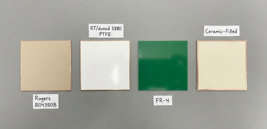
The high-speed PCB material industry has a couple of layers. Mid-loss options like Isola FR408HR and Panasonic Megtron 4 provide a decent increase over regular FR -4, but the price increase is moderate, and they are fine in projects up to about 10-16 Gbps. When you are pushing to 25-56Gbps, consider low-loss mates, such as Megtron 6, Isola I-Tera MT40, or Tachyon 100G - they tend to reach Df values of 0.003-0.005 at 10GHz. To have the very best, highest-end 100+ Gbps stuff, you will also require ultra-low-loss boards that are near PTFE performance.
Material selection should be driven by channel loss budget analysis, not by blanket specifications. Some traces are short enough that even standard FR-4 provides adequate margin; others need premium materials. Analyze each critical net individually.
Copper Roughness Control and Thermal Properties
Copper roughness contributes significantly to conductor loss at high frequencies — the same skin effect phenomenon that concerns RF designers. For high-speed digital at 25+ Gbps, the difference between standard and reverse-treated (low-roughness) copper foil can be 0.2-0.4 dB/inch, which adds up quickly on 10+ inch trace lengths.
Thermal properties of high-speed laminates matter for reliability, especially in systems with high power dissipation. Glass transition temperature (Tg), decomposition temperature (Td), and CTE (coefficient of thermal expansion) must be adequate for the assembly reflow profile and the product’s operating temperature range. Most premium high-speed materials offer improved thermal properties alongside their electrical benefits.
Material Trade-Offs for Cost, Reliability, and Speed
Material selection for high-speed PCB manufacturing involves balancing multiple factors. Premium materials reduce signal loss but increase board cost by 2-5x. They may also affect fabrication yield if the manufacturer is not experienced with the specific material. Some ultra-low-loss materials have lower Tg or more challenging processing requirements than standard FR-4.
The most cost-effective approach is to analyze your specific link budgets and select the minimum material performance that provides adequate margin. Use a hybrid stackup if only certain layers require premium materials. And always verify that your fabricator has production experience with your chosen material — an unfamiliar material can introduce yield issues that negate the cost savings of choosing a less expensive option.
Pro-Tip: Run a channel loss simulation (using tools like Keysight ADS, Ansys HFSS, or even free tools like Saturn PCB Toolkit) before selecting materials. The simulation will tell you exactly how much loss budget you have and what material performance level you need — no guessing required.
Proven Design Approaches for Reliable High Speed PCBs
Impedance Control, Differential Pair Routing, and Layer Stackup
So all high-speed signals must be implemented as a controlled-impedance transmission line. Single-ended signals are typically driven to 50 ohms; differential pairs are driven to 85 ohms, 90 ohms, or 100 ohms, depending on the interface standard. The geometries of the traces that reach those targets are determined by the stack-up design layer thicknesses, dielectric constants, and copper weights.
In routing pairs of differential traces, you must maintain the distance between the + and the – traces uniform throughout. The length overlap among pairs (intra-pair skew) must be comparable to a few mils in such multi-gigabit signals. Inter-pair skew, or the difference between various pairs of differentials in a bus, is a little looser, but you still need to consider it in parallel interfaces such as DDR5.
An excellent high-speed stack-up lays all the signal layers immediately adjacent to a solid reference plane and the most important signals are on the layers nearest to the board center to ensure the maximum amount of shielding. The use of signal and ground/power planes alternating in the stack-up ensures that the return path remains solid.
Via Back-Drilling and Crosstalk Mitigation Techniques
Via stubs are the unused portion of a through-hole via extending past the target layer — create quarter-wave resonances that cause deep notches in the frequency response. For a standard 62-mil thick board, the via stub resonance falls around 12 GHz, right in the middle of the frequency band needed for 25 Gbps signals.
Back-drilling removes the stub by mechanically drilling away the unused via barrel from one or both sides of the board. The process requires precise depth control (±4 mils typical) to ensure complete stub removal without damaging the target signal layer. For designs above 10 Gbps, back-drilling is nearly always worthwhile.
Crosstalk mitigation combines several techniques: maintaining adequate trace spacing (at least 3x the dielectric height between the trace and its reference plane), using ground-referenced vias between signal via pairs, inserting ground traces or copper pours between adjacent high-speed channels, and avoiding parallel routing of aggressor and victim traces over long distances.
Simulation and DFM Integration Early in Design
Pre-layout simulation is not optional for high-speed designs; it is the foundation of a successful board. Channel simulation validates that the combination of material, stackup, trace geometry, via transitions, and connectors delivers adequate signal quality for the target data rate. This analysis should happen before routing begins, not after.
DFM integration during the design phase ensures that your simulated design is actually manufacturable. Trace widths and spacings must fall within the fabricator’s capability range for the chosen material and copper weight. Via geometries must be compatible with the drill aspect ratios that the fabricator can reliably produce. Back-drill depths must have an adequate margin for the fabricator’s process capability. Early DFM review avoids the painful cycle of discovering manufacturing constraints after the design is complete.
Precision Manufacturing for Flawless High Speed PCBs
Tight Tolerance Etching, Drilling, and Registration Processes
High-speed PCB manufacturing demands fabrication precision that standard boards do not require. Trace width tolerance of ±0.5 mil or better ensures impedance stays within the specified window. Layer-to-layer registration of ±2 mils or better maintains consistent impedance by keeping signal traces properly aligned with their reference planes.
Drill positional accuracy is determined via-to-pad alignment and affects the quality of back-drilled vias. For back-drilling, the drill must stop within ±4 mils of the target depth, which is close enough to remove the stub without penetrating the signal layer. This requires Z-axis controlled drilling equipment with real-time depth monitoring.
Etching profile controls the cross-sectional shape of the finished trace and affects the impedance accuracy beyond what trace width alone determines. Advanced etching processes that minimize undercutting produce more rectangular profiles that better match the impedance calculated by design tools.
Surface Finish and Lamination for Minimal Signal Degradation
Surface finish selection impacts high-speed signal performance at the component interface. ENIG provides a flat, reliable surface for fine-pitch BGAs but introduces magnetic loss from the nickel layer that can be measured at frequencies above 5 GHz. Immersion silver offers lower loss and excellent flatness but has a shorter shelf life. OSP is the lowest-cost, lowest-loss option for boards assembled shortly after fabrication.
Lamination quality directly affects impedance control and dielectric loss. Precise resin flow control maintains consistent dielectric thickness between signal layers and reference planes. Inadequate resin flow leaves voids that change the effective dielectric constant; excessive flow thins the dielectric and shifts impedance.
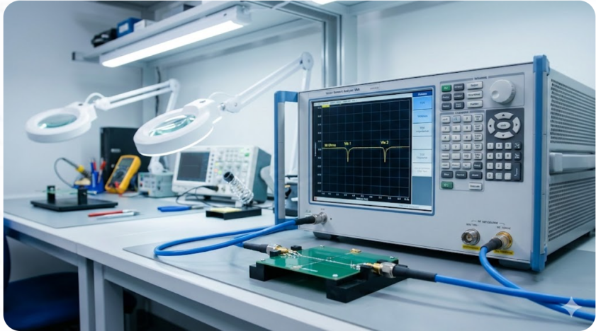
Comprehensive Testing Including TDR and Eye Diagram Analysis
TDR (Time Domain Reflectometry) testing on impedance coupons verifies that the fabricated impedance matches the design target. For high-speed boards, ±7% or ±5% impedance tolerance may be specified depending on the link budget analysis.
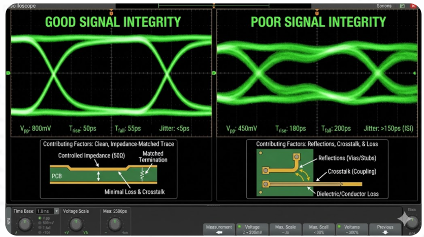
Eye diagram measurements on dedicated test channels provide the most comprehensive validation of high-speed PCB quality. By driving a PRBS pattern through a fabricated test structure and measuring the received eye diagram, you can directly assess the combined impact of all loss, reflection, and coupling mechanisms on signal quality. This measurement is the ultimate proof that the board will support the target data rate. Leading-edge high-speed PCB design services providers include TDR and insertion loss data as standard quality documentation, giving designers confidence that their boards will perform as simulated.
JLCPCB’s Specialized Capabilities in High-Speed PCB Production
Premium Material Partnerships and Cutting-Edge Fabrication Lines
JLCPCB maintains partnerships with leading laminate manufacturers to offer a comprehensive range of high-speed materials, from enhanced FR-4 through ultra-low-loss options. Combined with precision fabrication equipment capable of the tight tolerances demanded by multi-gigabit signal integrity, JLCPCB provides end-to-end high-speed PCB manufacturing capability.
Expert DFM Reviews Tailored for High Speed Designs
High-speed designs require DFM attention beyond standard board checks. JLCPCB’s DFM process evaluates stackup feasibility, impedance achievability with available materials, back-drill depth requirements, and other high-speed-specific factors. This specialized review catches issues that generic DFM tools miss, preventing production delays and performance surprises.
Scalable Manufacturing with Proven High-Yield Results

From prototype validation to high volume production, JLCPCB maintains the PCB performance solid. The same material specifications, process control, and quality check will work at each scale, and thus your prototype-tested design will run the same when you spin it up to thousands of boards.

Frequently Asked Questions (FAQ)
What qualifies as a high-speed PCB?
Any PCB where signal interconnect behavior significantly affects signal quality qualifies as high-speed. In practice, this includes boards with data rates above 1 Gbps, rise times below 1 ns, or interfaces like PCIe Gen 3+, USB 3.0+, DDR4/5, or multi-gigabit Ethernet.
When should I switch from FR-4 to a premium laminate?
When channel simulation shows that FR-4 loss consumes too much of your link budget to maintain adequate eye opening, as a rough guideline, interfaces above 10 Gbps typically benefit from enhanced or low-loss materials, and interfaces above 25 Gbps almost always require them.
How important is back-drilling for high-speed designs?
Very important for through-hole vias carrying signals above approximately 8-10 Gbps. The via stub resonance can create deep notches in the channel frequency response that dramatically degrade signal quality. Back-drilling removes this resonance and is standard practice for 25+ Gbps designs.
What impedance tolerance should I specify?
Standard ±10% is adequate for most high-speed digital applications up to about 10 Gbps. For 25+ Gbps, specify ±7% or ±5% based on your link budget analysis. Tighter tolerance increases fabrication cost, so match the spec to your actual performance requirement.
Can high-speed and standard designs coexist on the same board?
Absolutely. Most modern boards combine high-speed interfaces (PCIe, DDR, Ethernet) with standard-speed control signals and power management. The key is applying high-speed design techniques only where needed, using controlled impedance and premium materials for the fast signals while routing standard signals conventionally.
Keep Learning
Building Reliable High-Speed Performance with Effective Timing Analysis
Key Takeaways Timing analysis is essential for high-speed PCBs — clean signals can still fail if they miss setup or hold windows. Focus on setup time, hold time, clock skew, and propagation delay to ensure reliable data sampling. Prioritize length matching, controlled impedance, and proper stackup to maintain positive timing margins. Combine static timing analysis with dynamic simulation for best results. Precision manufacturing is critical — small variations in impedance or dielectric thickness can d......
Low Loss PCBs : Advanced Materials for Superior High-Speed Signal Performance
Key Takeaways Low Loss PCBs using advanced materials like Rogers RO4003C, RO4350B, and PTFE laminates deliver superior signal integrity by dramatically reducing dielectric loss at multi-gigahertz frequencies. Ideal for 5G, mmWave, RF, and high-speed digital designs, these boards offer significantly lower insertion loss, stable impedance, and better thermal performance compared to standard FR4. By choosing the right low-loss laminate and partnering with experienced manufacturers like JLCPCB, engineers ......
How to Reduce Insertion Loss for Better High-Speed PCB Performance
Key Takeaways Reducing insertion loss is essential for achieving reliable high-speed PCB performance. By selecting low-loss materials with lower Df, optimizing trace routing and stackup design, minimizing via transitions, using smoother copper foils, and applying precision manufacturing techniques, designers can significantly lower both dielectric and conductor losses. These strategies help maintain better signal integrity, wider eye openings, and higher data rates in multi-gigabit designs. Have you e......
How to Create the Perfect PCB Stackup for High-Speed and Reliable Designs
Key Takeaways A well-designed PCB stackup is the foundation of high-speed, reliable designs, determining signal integrity, controlled impedance, and EMI performance. Use symmetrical layers with adjacent reference planes, proper dielectric spacing, and copper balancing to avoid warpage and crosstalk. Choose standard FR4 for <3 GHz or low-loss materials (Megtron 6, Rogers) for higher speeds, and work closely with manufacturers for optimal results. Mastering your stackup is essential for high-speed succe......
Achieving Reliable High-Speed Performance with PCB Transmission Lines
Key Takeaways PCB Transmission Lines are essential for reliable high-speed PCB performance in USB 3.0, PCIe, DDR4, and RF designs, turning traces into controlled-impedance structures that eliminate reflections, crosstalk, and attenuation. Select microstrip, stripline, or GCPW geometries with accurate calculations, continuous reference planes, mitered bends, and 3W spacing, then rely on precise etching, copper profile control, and TDR testing at JLCPCB for consistent results from prototype to volume pr......
Backdrill Vias: Enhancing Signal Integrity in High-Speed PCBs
Key Takeaways Backdrill vias remove unused copper stubs from plated through-hole vias, shortening the residual stub to under 0.15 mm (6 mils). This eliminates impedance discontinuities, reflections, and resonances in high-speed signals above 5–10 Gbps. It delivers better return loss, insertion loss, lower jitter, and clearer eye diagrams — all while keeping simple stack-ups and far lower cost than blind/buried vias. Use backdrilling for any stub longer than 15 mils (0.381 mm), especially on boards thi......