
Surface Mount Technology Explained: A Practical SMT Guide for PCB Assembly
13 min
- What Is Surface Mount Technology?
- SMT vs SMD: What Is the Difference?
- Advantages of Surface Mount Technology
- Surface Mount Technology Process
- SMT Components and Package Sizes
- Surface-Mount Technology vs Through-Hole
- SMT Assembly Design Guidelines and DFM Checklist
- Common SMT Soldering Defects and How to Fix
- What Affects SMT Assembly Cost?
- What Files Are Needed for SMT PCB Assembly?
- SMT Quality Standards and IPC Classes
- Conclusion
- FAQs about Surface Mount Technology
Surface Mount Technology (SMT) is the standard method used to assemble most modern printed circuit boards. Instead of inserting component leads through drilled holes, SMT places small surface-mount devices directly onto PCB pads and solders them through a controlled reflow process.
Today, SMT is used in everything from smartphones and computers to automotive electronics and industrial equipment because it enables smaller devices, higher component density, faster production, and lower assembly costs.
In this guide, you will learn:
- What Surface Mount Technology means
- The difference between SMT and SMD
- How the SMT PCB assembly process works
- Common SMD package sizes and IC packages
- SMT vs through-hole technology
- SMT design guidelines for better manufacturability
- Common SMT soldering defects and how to prevent them
- How to reduce SMT assembly cost
What Is Surface Mount Technology?
Surface Mount Technology (SMT) is a PCB assembly method in which electronic components are mounted directly onto the surface pads of a printed circuit board (PCB), rather than inserted through drilled holes as in traditional through-hole technology (THT).
In an SMT assembly process, solder paste is first applied to designated PCB pads, after which surface-mount devices (SMDs) are accurately placed using automated pick-and-place equipment. The board then passes through a reflow oven, where the solder melts and forms reliable electrical and mechanical connections between the components and the PCB.
Today, SMT is the dominant assembly technology used in consumer electronics, industrial control systems, telecommunications equipment, automotive electronics, and many other electronic products. Compared with through-hole assembly, SMT enables higher component density, smaller board sizes, faster production, and greater suitability for automated manufacturing.
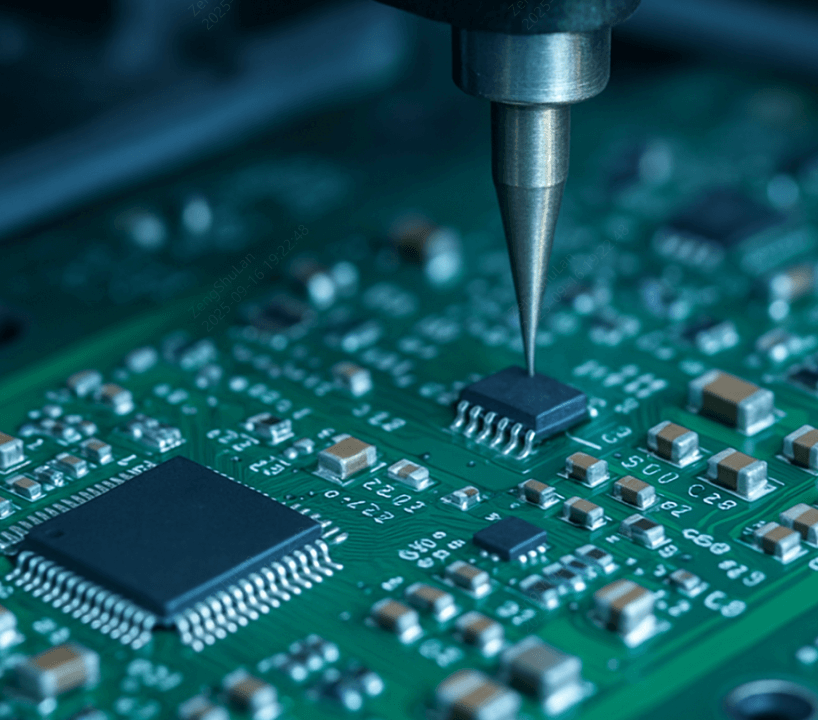
Figure: Robotic arm placing an integrated circuit on a PCB during automated SMT assembly process
SMT vs SMD: What Is the Difference?
SMT describes the assembly technology used to mount components onto a PCB, whereas SMD refers to the components designed for that assembly method.
| Term | Full Name | Meaning | Examples |
|---|---|---|---|
| SMT | Surface Mount Technology | The assembly technology used to mount electronic components directly onto PCB surface pads | Solder paste printing, pick-and-place assembly, reflow soldering |
| SMD | Surface Mount Device | An electronic component designed to be mounted directly onto PCB surface pads | Chip resistors, MLCC capacitors, QFN packages, BGA packages |
Advantages of Surface Mount Technology
- Higher Component Density: SMT components occupy less board space, allowing more functionality to be integrated into the same PCB area.
- Lower Assembly Costs at Scale: Automated pick-and-place and reflow soldering processes reduce labor requirements and improve manufacturing efficiency in medium- and high-volume production.
- Better High-Frequency Performance: Shorter interconnect lengths help reduce parasitic inductance and capacitance, improving signal integrity in high-speed and RF applications.
- Support for Advanced IC Packages: SMT enables the use of modern package types such as BGA, QFN, CSP, and LGA devices that are not practical for through-hole assembly.
- Faster and More Consistent Manufacturing: Automated assembly processes improve repeatability, reduce human error, and support high-volume production.
- Compatibility with Automated Inspection: SMT assembly works effectively with inspection technologies such as AOI, SPI, and X-ray inspection, helping improve quality control and defect detection.
Surface Mount Technology Process
The SMT assembly process combines automated equipment, precision soldering, and multiple quality-control stages to assemble electronic components onto a printed circuit board (PCB). While production lines may vary depending on product requirements, most SMT PCB assemblies follow the same core workflow outlined below.
1. Solder Paste Printing
The process begins with solder paste printing. A stainless-steel stencil is precisely aligned with the PCB, allowing solder paste to be deposited onto designated surface-mount pads. The amount and consistency of solder paste are critical, as excessive or insufficient paste can lead to defects such as solder bridges, opens, or weak solder joints during reflow.
2. Solder Paste Inspection (SPI)
After printing, the SMT production line performs Solder Paste Inspection (SPI). Using 3D measurement systems, SPI verifies the height, area, and volume of the deposited solder paste. Detecting printing defects at this stage helps prevent assembly issues later in the process and improves overall manufacturing yield.
3. Pick-and-Place Assembly
Next, automated pick-and-place machines position Surface Mount Devices (SMDs) onto the solder-pasted PCB pads according to assembly placement data. Modern equipment can place thousands of components per hour with high accuracy, ranging from tiny chip resistors and capacitors to complex integrated circuit packages.
4. Reflow Soldering
Once all components are placed, the PCB passes through a reflow oven with a carefully controlled temperature profile. The solder paste melts and forms both electrical and mechanical connections between the components and the PCB. Proper temperature control is essential to ensure reliable solder joints while avoiding thermal damage to sensitive components.
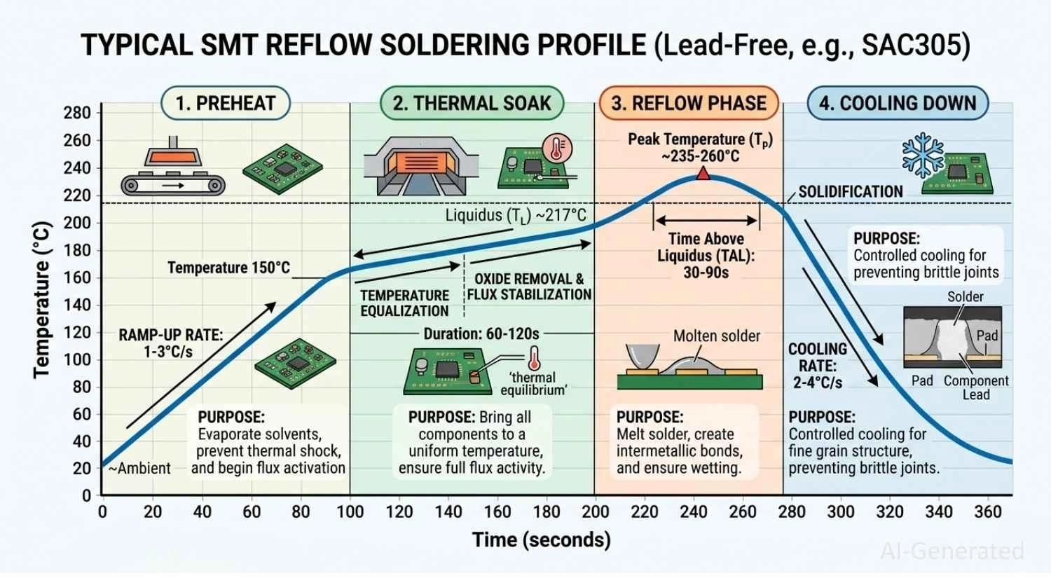
Figure: Lead-free SMT reflow soldering temperature profile
5. Inspection and Testing
After reflow soldering, the assembled PCB undergoes inspection and testing to verify assembly quality.
Automated Optical Inspection (AOI) is commonly used to detect visible defects such as missing components, polarity errors, solder bridges, and tombstoning.
For assemblies containing packages with hidden solder joints, such as BGAs, X-ray inspection may be used.
Electrical verification methods, such as flying probe testing, can further confirm connectivity and assembly integrity.
SMT Components and Package Sizes
1. Passive SMD Components
Passive components such as resistors, capacitors, inductors, and ferrite beads are among the most common components used in SMT assembly. They are typically manufactured in standardized package sizes, with smaller packages enabling higher component density and more compact PCB designs.
Common passive component package sizes include:
| Package Size | Dimensions (mm) |
|---|---|
| 01005 | 0.4 × 0.2 |
| 0201 | 0.6 × 0.3 |
| 0402 | 1.0 × 0.5 |
| 0603 | 1.6 × 0.8 |
| 0805 | 2.0 × 1.25 |
| 1206 | 3.2 × 1.6 |
Note
JLCPCB's advanced SMT assembly service can support 01005 packages.
2. SMT IC Packages
Integrated circuits (ICs) are available in a variety of SMT package types, each optimized for different pin counts, thermal requirements, and manufacturing needs.
Common SMT IC packages include:
- SOIC (Small Outline Integrated Circuit)
- QFP (Quad Flat Package)
- QFN (Quad Flat No-Lead)
- BGA (Ball Grid Array)
- TQFP (Thin Quad Flat Package)
- LQFP (Low-profile Quad Flat Package)
Among these package types, QFN and BGA packages are widely used in modern high-density PCB designs due to their compact footprint and improved electrical performance.
Note
Component Orientation and Polarity: During SMT assembly, polarized components such as diodes, LEDs, tantalum capacitors, and electrolytic capacitors must be placed with the correct orientation. Incorrect polarity can cause circuit malfunction, component damage, or assembly failure. For this reason, assembly machines and inspection systems verify component orientation as part of the manufacturing process.
Surface-Mount Technology vs Through-Hole
| Aspect | SMT | Through-Hole Technology |
|---|---|---|
| Component mounting | Components are soldered directly onto PCB surface pads | Component leads pass through drilled holes and are soldered on the opposite side |
| Board density | Higher density and suitable for compact or double-sided PCB layouts | Lower density because holes and lead spacing require more board area |
| Mechanical strength | Lower mechanical strength for large or stressed parts | Stronger mechanical support, especially for connectors and heavy components |
| Assembly speed | Highly automated and suitable for mass production | Slower and often requires manual or selective soldering |
| Cost | Lower cost at medium to high volume | Higher cost due to drilling, manual handling, and slower assembly |
| Best used for | Phones, laptops, IoT devices, compact electronics | Connectors, transformers, power components, rugged prototypes |
Choose SMT when:
- The PCB must be compact and lightweight
- The design uses high pin-count ICs such as QFN, BGA, or QFP
- You need automated assembly for medium or high-volume production
- High-frequency performance matters
- Both sides of the PCB need components
Choose through-hole when:
- The component needs strong mechanical support
- The design includes connectors, switches, transformers, or large capacitors
- The PCB is used in high-vibration environments
- Manual assembly or educational prototyping is the priority
SMT Assembly Design Guidelines and DFM Checklist
Before submitting a PCB for SMT assembly, review the following design-for-manufacturing (DFM) requirements:
1. Use IPC-7351-compliant footprints and land patterns.
2. Ensure proper solder mask clearance and pad spacing for fine-pitch devices to reduce solder bridging.
3. Match stencil aperture design to pad geometry and component pitch.
4. Add clear polarity and orientation markings for diodes, LEDs, electrolytic capacitors, and IC pin 1 indicators.
5. Use symmetrical pad layouts and balanced thermal reliefs to minimize tombstoning risks.
6. Maintain adequate component-to-edge clearance (typically 3–5 mm) for depanelization and handling.
7. Avoid placing tall components near small passive devices where shadowing or placement interference may occur.
8. Provide global and local fiducial marks for accurate machine alignment.
9. Ensure silkscreen markings do not overlap pads or solder mask openings.
10. Add accessible test points for power rails, programming interfaces, and critical signals.
11. Verify component availability, package compatibility, and approved substitutes before production.
12. Review panelization requirements, tooling holes, and breakaway features when applicable.
13. Export accurate BOM, Gerber, and pick-and-place (CPL/XY) files before ordering assembly.
Common SMT Soldering Defects and How to Fix
| Defect | Cause | How to Prevent or Fix |
|---|---|---|
| Tombstoning | Uneven heating or unequal solder paste volume on small passives | Balance pad design, stencil aperture, and reflow profile |
| Solder bridge | Excess solder paste or insufficient spacing between pins | Optimize stencil openings, reduce paste volume, inspect fine-pitch pads |
| Cold joint | Insufficient heat or poor wetting | Adjust reflow profile and verify solder paste condition |
| Misalignment | Pick-and-place calibration errors or poor fiducials | Add fiducials and calibrate placement equipment |
| Open joint | Insufficient solder paste or poor pad wetting | Check paste printing, pad finish, and component coplanarity |
| Voiding | Trapped flux or poor thermal pad design | Use proper thermal pad stencil design and reflow settings |
What Affects SMT Assembly Cost?
1. Component Count
The total number of components directly affects assembly costs. More placements require longer machine runtime, additional inspection, and increased production time.
For example, a board with 1,000 component placements typically costs more to assemble than a board with 200 placements, even if both boards have similar dimensions.
2. Component Type and Package Size
Certain package types require higher placement accuracy and more advanced inspection processes. Fine-pitch components such as BGAs, QFNs, CSPs, and ultra-small passive devices (0201 or 01005) can increase assembly complexity and cost.
Additional processes such as X-ray inspection may also be required for packages with hidden solder joints.
3. Number of Unique Components
A larger variety of component types increases feeder setup time, inventory management requirements, and machine changeovers.
Using fewer unique part numbers can improve assembly efficiency and reduce production costs, especially in medium- and high-volume manufacturing.
4. Single-Sided vs. Double-Sided Assembly
Boards assembled on both sides typically require additional setup, handling, and reflow processes.
Compared with single-sided designs, double-sided SMT assembly generally involves longer production cycles and higher manufacturing costs.
5. Panelization Efficiency
Efficient panelization improves machine utilization and reduces handling time.
6. Inspection and Testing Requirements
Quality assurance processes contribute to overall assembly costs.
Depending on the product requirements, manufacturers may perform:
- Automated Optical Inspection (AOI)
- X-ray Inspection
- In-Circuit Testing (ICT)
- Functional Testing (FCT)
Products requiring advanced inspection methods generally incur higher assembly costs.
7. Production Volume
Assembly setup costs are distributed across the total production quantity.
Higher production volumes generally reduce the assembly cost per board, while low-volume prototype runs often have higher per-unit costs because setup and programming expenses are shared across fewer units.
Real-World Example
Consider two PCB assemblies of similar size:
- Board A contains 500 standard 0603 passive components and several SOIC packages.
- Board B contains only 250 components but includes multiple fine-pitch BGAs, QFNs, and requires X-ray inspection.
Although Board B has fewer components, its assembly cost may be significantly higher due to increased placement precision requirements, longer setup times, and additional inspection processes.
What Files Are Needed for SMT PCB Assembly?
For SMT PCB assembly, manufacturers usually need:
- Gerber files for PCB fabrication
- BOM file listing part numbers, quantities, and designators
- CPL or pick-and-place file showing component coordinates and rotation
- Assembly drawing if polarity or special placement needs clarification
- Testing requirements if functional testing is needed

- If you are preparing a board for SMT assembly, JLCPCB supports online DFM checks, component sourcing, SMT stencil options, AOI/X-ray inspection, and assembly for package sizes down to 01005.
- Upload your Gerber, BOM, and CPL files to check pricing and manufacturability now.
SMT Quality Standards and IPC Classes
The electronics manufacturing industry commonly follows IPC standards to define acceptable assembly quality and design practices.
Two widely referenced standards include:
- IPC-A-610 – Defines the acceptability criteria for electronic assemblies, including solder joints, component placement, and workmanship requirements.
- IPC-7351 – Provides guidelines for SMT land pattern and footprint design to improve manufacturability and assembly reliability.
- IPC J-STD-001 – Specifies the requirements for soldered electrical and electronic assemblies, including materials, processes, and inspection criteria.
IPC Class 1 – General Electronic Products
Class 1 applies to general consumer products where the primary requirement is functional performance. Cosmetic imperfections may be acceptable provided they do not affect basic operation.
Typical applications include:
- Consumer electronics
- Toys
- Low-cost commercial products
IPC Class 2 – Dedicated Service Electronic Products
Class 2 is intended for products that require reliable and continuous performance throughout their expected service life.
Typical applications include:
- Industrial equipment
- Telecommunications systems
- Networking devices
- Commercial electronics
IPC Class 3 – High-Reliability Electronic Products
Class 3 represents the highest workmanship and reliability requirements. These products must continue operating under demanding conditions where failure could result in significant consequences.
Typical applications include:
- Aerospace systems
- Medical devices
- Mission-critical control systems
Industry Practice: Most commercial SMT assemblies are manufactured to IPC Class 2 requirements because they provide a practical balance between reliability, manufacturability, and cost
Conclusion
Surface Mount Technology has become the foundation of modern PCB assembly because it enables smaller board sizes, higher component density, faster automated production, and lower assembly costs.
For designers and engineers, successful SMT assembly is not only about choosing SMD components. It also requires proper footprint design, solder paste control, component orientation, DFM review, inspection, and cost optimization. By understanding the SMT process, common defects, IPC standards, and required assembly files, you can reduce manufacturing risks and improve first-pass yield.
Whether you are building a prototype or preparing for mass production, designing with SMT best practices helps ensure a more reliable, manufacturable, and cost-effective PCB assembly.
FAQs about Surface Mount Technology
Q: What does SMT stand for?
SMT stands for Surface Mount Technology, a PCB assembly method where components are mounted directly onto the surface of a printed circuit board.
Q: Is SMT better than through-hole technology?
SMT is better for compact, automated, high-density PCB assembly. Through-hole technology is better for parts that need strong mechanical support, such as connectors and large power components.
Q: What is the smallest SMT component size?
01005, measuring about 0.4 mm × 0.2 mm, is among the smallest commonly used passive SMT package sizes.
Q: Can SMT components be soldered by hand?
Yes, larger SMT packages such as 0805, 1206, SOIC, and some QFP parts can be hand-soldered. Very small packages such as 0201, 01005, BGA, and QFN are usually better suited for automated assembly
Popular Articles
• Common PCB Assembly Methods and Soldering Techniques Explained
• What Is BGA Void? Causes, IPC Limits, and Solutions
• SMD Soldering Tools You Need: Complete Guide from Beginner to Pro
• Reflow Soldering: Everything You Need to Know
• SMT Assembly Process Explained and Equipment Used: A Step-by-Step Guide to PCBA Manufacturing
Keep Learning
12 Professional Soldering Tips and Tricks Every Beginner Should Know
Soldering is not merely "gluing" metal; it is a metallurgical process that creates an intermetallic compound (IMC). This molecular bond ensures the electrical and mechanical integrity of your device. A poor joint might pass a quick visual check but will inevitably fail under vibration or thermal stress, leading to "ghost" bugs and hardware failures. These soldering tips and tricks focus on practical, repeatable techniques used in professional electronics soldering—from correct heat transfer and flux u......
Solder Melting Point Guide: Chart, Alloy Types, and Reflow Considerations
In the precise world of electronics manufacturing, a difference of just a few degrees can mean the distinction between a perfect, reliable solder joint and a catastrophic "cold" joint failure. While many hobbyists view soldering simply as "melting metal to stick things together," professional PCB assembly requires a nuanced understanding of thermodynamics. The solder melting point is not simply a single value listed in a datasheet; it is a decisive limit that determines the choice of components, the s......
The Ultimate Guide to Solder Flux: Everything You Should Know Before Soldering PCB
Soldering is needed to make almost all electronic devices. Adding solder alone won't make a joint that is strong, clean, and sound from a metallurgical point of view. Solder flux is a very important part of the process that comes in here. If you want to do your job better and make it more reliable, you need to know a lot about soldering flux, whether you're an engineer, a professional technician, or just a hobbyist. This article goes into a lot of detail about solder flux, including what it is, how it......
Common PCB Assembly Methods and Soldering Techniques Explained
Whether you're designing your first prototype or scaling up to production, understanding PCB assembly methods and soldering techniques is crucial to achieving reliable, high-performance circuit boards. Modern PCBA primarily relies on Surface Mount Technology (SMT) and Through-Hole Technology (THT)—each offering unique advantages for component density, durability, and manufacturability. In this guide, we'll break down the major PCB assembly methods, key soldering techniques such as reflow and wave sold......
Flex PCB Assembly Guide: Process, Challenges, and Solutions
Flexible Printed Circuit Boards (Flex PCBs) are the foundational technology enabling the compact, innovative design of modern electronics. Because of their ability to bend and fold, they power devices from smart wearables to compact medical instruments where traditional rigid printed circuit boards (Rigid PCBs) can't be used. Achieving a functional electronic circuit from the raw plastic film demands special expertise, with flexible PCB assembly (FPCA) representing the crucial final step in this trans......
SMD Rework Guide: Tools, Temperatures, and Techniques That Prevent PCB Damage
From replacing a burned regulator to correcting wrong component values or removing solder bridges on fine-pitch ICs, SMD rework is an essential skill in electronics manufacturing and prototyping. It allows engineers to repair assembly defects, implement design changes, and recover valuable PCBs without the cost and delay of building new boards. In this guide, you will learn: What SMD rework is Common rework scenarios Tools and temperatures Safe removal and installation Package-specific techniques Real......