
Quad Flat Package (QFP): The Engineer's Guide to Design, Assembly and Thermal Management
13 min
- What is QFP Package?
- Quad Flat Package (QFP) Types and Selection Guide
- Quad Flat Package (QFP) Structure and Material Science Explained
- QFP Package PCB Footprint & Land Pattern Guidelines (IPC-7351B)
- Advanced Thermal Management for QFP Package
- SMT Assembly of Quad Flat Package (QFP): Challenges and Solutions
- QFP Component Sourcing and Assembly Reliability Standards
- FAQ about Quad Flat Package (QFP)
- Conclusion: Quad Flat Package (QFP)
What is QFP Package?
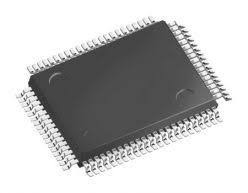
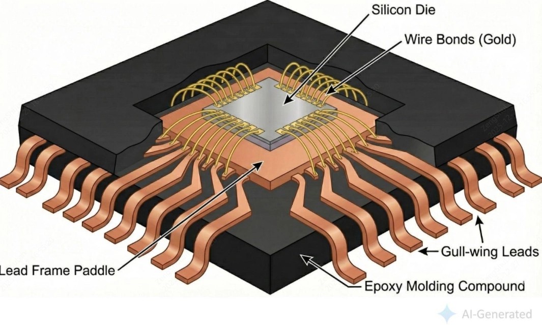
The Quad Flat Package (QFP) is one of the most popular surface mount technology (SMT) package formats throughout the history of electronic manufacturing. After it became standard in the 1980s, the QFP has been the industry standard for integrated circuits (ICs) with moderate to high pin counts that typically range from 32 to 304 pins, so it was a good alternative for simple SOIC packages and complex Ball Grid Arrays (BGAs) at the same time.
Defined by its "gull-wing" leads extending from all four sides of a square or rectangular body, the QFP offers a unique balance of high I/O density, cost-effective manufacturing, and - crucially for debugging - visual inspectability. Unlike BGAs, where solder joints are hidden, QFP leads are visible, allowing for straightforward optical inspection and rework.
Quad Flat Package (QFP) Types and Selection Guide
While "QFP" is the generic term, selecting the specific variant impacts the Z-height of your product and the thermal strategy of your PCB.
Comparison Table: QFP Package Types
| Variant | Full Name | Body Height (Max) | Pin Count Range | Typical Pitch | Thermal θJA (Still Air) | Primary Use Case |
|---|---|---|---|---|---|---|
| LQFP | Low-Profile Quad Flat Package | 1.60 mm | 32 – 256 | 0.50 mm | 35 – 50 °C/W | Microcontrollers, Consumer Electronics |
| TQFP | Thin Quad Flat Package | 1.20 mm | 32 – 176 | 0.40 – 0.80 mm | 40 – 55 °C/W | Mobile Devices, FPGA (Low Power) |
| PQFP | Plastic Quad Flat Package | 3.40 mm | 64 – 304 | 0.65 mm | 30 – 45 °C/W | Legacy Systems, Industrial Control |
| BQFP | Bumpered Quad Flat Package | 3.80 mm | 84 – 196 | 0.635 mm | 35 – 50 °C/W | Socketed Prototyping (Bumpered corners) |
Note
Thermal values are typical ranges under JEDEC still-air conditions and vary by vendor and PCB design.
Low Profile Quad Flat Package (LQFP)
The LQFP is the workhorse of the industry (JEDEC MS-026).
LQFP (Low-Profile Quad Flat Package) reduces body height while keeping the same general lead geometry. This lower profile helps when vertical clearance inside the enclosure is limited, without introducing major changes to PCB layout or assembly processes. LQFP is often chosen in designs where space above the board is constrained but serviceability is still required.
- Height: Standardised at a 1.4mm nominal body thickness.
- Pitch Options: You can choose from sizes 0.8mm, 0.65mm, 0.5mm, and 0.4mm.
- Application: Ideal for standard microcontrollers (e.g., STM32 series found in the JLCPCB Parts Library) where vertical space is not critically constrained.
- Thermal: Standard LQFP θJC is roughly 25-35°C/W.
Thin Quad Flat Package (TQFP)
The TQFP is designed for portable applications like laptops and tablets.
TQFP (Thin Quad Flat Package) further reduces package thickness and overall mass. While this helps in compact designs, the thinner body and finer mechanical tolerances make TQFP slightly less forgiving during handling and soldering. In practice, this means tighter process control and less tolerance for board warpage or mechanical stress.
- Height: Reduced to 1.0mm total body thickness.
- Constraint: The thinner packaging results in a smaller amount of mold compound above the die, which slightly decreases thermal mass and increases the chance of the package getting warped during reflow if the cooling profile is too aggressive.
Plastic Quad Flat Package (PQFP)
PQFP Package (Plastic Quad Flat Package) is the traditional, standard-profile option. It offers a thicker body and robust lead structure, making it mechanically forgiving during handling and assembly. This makes PQFP well suited for industrial and automotive boards where mechanical stress, vibration, or repeated rework are expected.
- Body thickness varies (2.0mm–3.8mm) and is used for high-pin-count devices (up to 304 pins).
Ceramic Quad Flat Package (CQFP)
Ceramic Quad Flat Package (CQFP) is a hermetically sealed package used in aerospace and military applications. It uses a glass frit seal or solder seal lid, rendering it impervious to moisture (MSL 1).
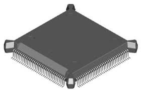
Bumpered Quad Flat Package (BQFP)
BQFP (Bumpered Quad Flat Package) adds protective bumpers at the corners of the package to shield the leads from mechanical damage during handling, insertion, or transportation. This makes BQFP particularly suitable for prototyping, socketed boards, and educational kits where repeated assembly or testing occurs. While electrically interchangeable with other QFP types, BQFP's mechanical features provide extra durability at the cost of slightly increased body height.
From a design perspective, these variants are interchangeable electrically but not mechanically. The choice between PQFP, LQFP, and TQFP is usually driven by enclosure height, mechanical stress expectations, and assembly robustness rather than signal integrity or pin functionality.
Quad Flat Package (QFP) Structure and Material Science Explained
To design for a QFP, one must understand what lies inside the molding compound. The reliability of the package during reflow and operation is dictated by the interaction between its internal materials.
Lead Frame Composition and CTE
The lead frame acts as both the electrical highway and the structural skeleton of the device.
- Copper Alloy (C194): Used in standard commercial applications for its superior electrical conductivity.
- Alloy 42 (Fe-Ni): Composed of 58% Iron and 42% Nickel. This material is critical for high-reliability applications because its Coefficient of Thermal Expansion (CTE) is approximately 4.0–4.5 ppm/°C, which closely matches the CTE of the silicon die (~2.6 ppm/°C). This matching minimizes the "thermomechanical stress" on the wire bonds during thermal cycling.
Wire Bonding and Interconnects
Inside the package, the connection between the silicon die and the lead frame is achieved via wire bonding.
- Gold Wire (Au): The gold standard (99.99% purity) with diameters of 18–25µm. It is resistant to oxidation and provides the most reliable intermetallic formation.
- Copper Wire (Cu): increasingly used to reduce costs. However, Cu wire requires a harder bonding force, which can damage fragile low-k dielectric layers on modern silicon if not controlled precisely.
Encapsulation and "Popcorning"
The body is formed using an Epoxy Molding Compound (EMC), typically filled 70-90% by weight with fused silica to lower the package's overall CTE (8–12 ppm/°C).
Technical Note on MSL
The hygroscopic nature of epoxy means it absorbs moisture. If a QFP absorbs moisture and is then subjected to 260°C reflow, the trapped water turns to steam, expanding rapidly. This causes package cracking or delamination, known as the "Popcorn Effect."
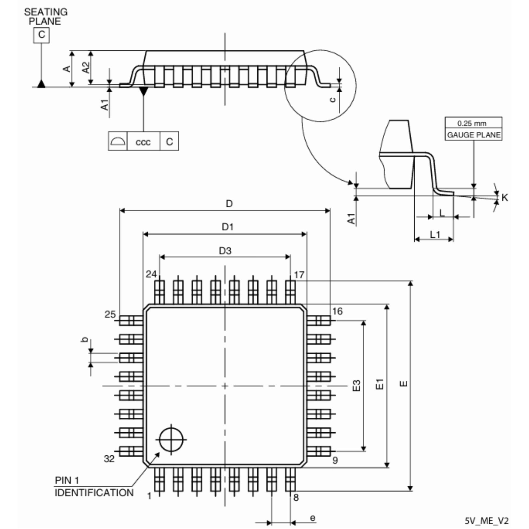
QFP Package PCB Footprint & Land Pattern Guidelines (IPC-7351B)
Designing a footprint for a QFP, especially at 0.5mm or 0.4mm pitch, leaves zero margin for error. A poor land pattern is the primary cause of solder bridging and open joints.
Land Pattern Geometry
According to IPC-7351B (Generic Requirements for Surface Mount Design), the land pattern must account for the "Toe," "Heel," and "Side" solder fillets.
- Toe Fillet: Crucial for allowing visual inspection.
- Heel Fillet: The most critical aspect for mechanical strength. The solder joint at the heel absorbs the majority of the shear stress during thermal expansion.
Design Rules for 0.5mm Pitch QFP
- Pad Width (X): 0.24mm – 0.28mm. (Do not exceed 0.30mm, or bridging risk increases).
- Pad Length (Y): 1.50mm – 1.60mm.
- Solder Mask Web: This is the sliver of solder mask between two adjacent pads. For a 0.5mm pitch, the gap between copper pads is roughly 0.22mm. JLCPCB requires a minimum solder mask bridge of 4 mil (0.1mm). If your mask opening is too large, the mask web will be too thin and may detach, leading to solder bridging.
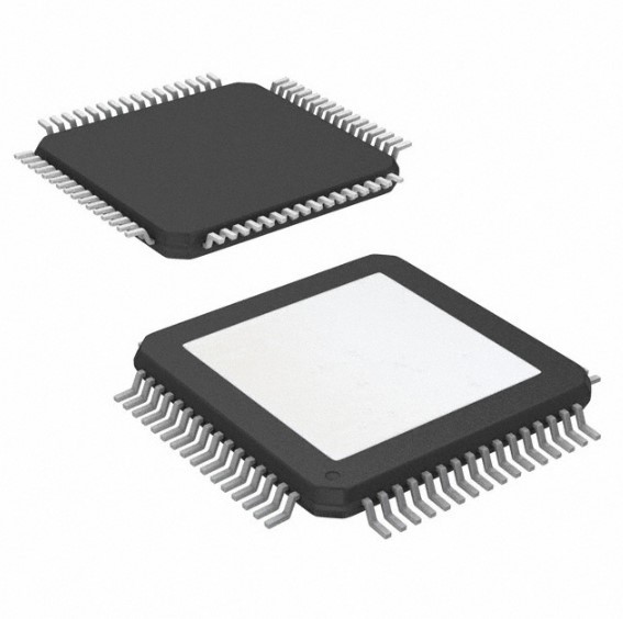
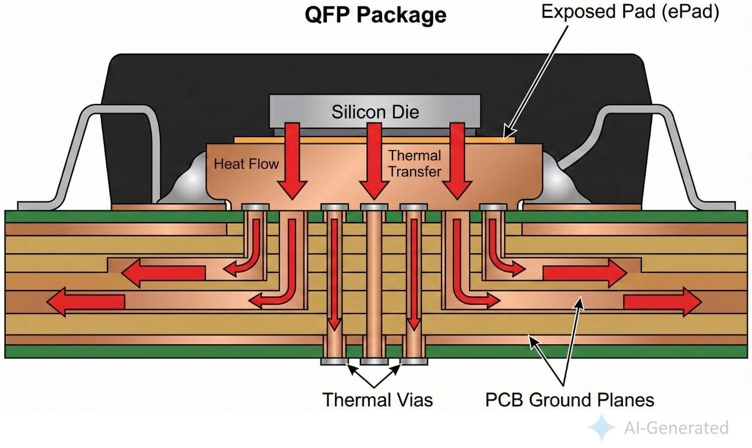
Thermal Vias and Exposed Pads (ePad)
Many modern QFPs (PowerQFP) feature an exposed die attach paddle (ePad) on the bottom. This must be soldered to the PCB ground plane.
- Via Design: Place a grid of thermal vias (0.3mm diameter) inside the ePad area.
- Tenting vs. Plugging: Do not leave vias open (un-tented) if they are large, as solder will wick down the hole, causing "solder voiding" on the main pad. To ensure high reliability, specify Via-in-Pad Plated Over (VIPPO) or capped vias within the Gerber files you submit to JLCPCB.
Advanced Thermal Management for QFP Package
For high-performance DSPs or FPGAs in QFP packages, calculating junction temperature is mandatory to prevent thermal throttling.
Understanding Thermal Resistance
- θJA (Junction-to-Ambient): The total resistance from the silicon die to the outside air.
- θJC (Junction-to-Case): Resistance from the die to the top of the plastic package.
- θJB (Junction-to-Board): Resistance from the die to the PCB.
The Formula:

Where TJ is Junction Temp, TA is Ambient Temp, and PD is Power Dissipated.
Enhancing Dissipation
If your calculated TJ exceeds 125°, you must lower θJA.
- Copper Weight: Switching from 1oz to 2oz inner copper layers can reduce θJB by spreading heat laterally across the PCB.
- Top-Side Heatsinks: Utilizing a thermally conductive adhesive to bond a heatsink to the top of the QFP reduces θJC.
- Airflow: Moving from still air to forced convection (1 m/s airflow) can reduce effective θJA by up to 20%.
SMT Assembly of Quad Flat Package (QFP): Challenges and Solutions
Assembly of fine-pitch QFPs (0.4mm and 0.5mm) is where the capabilities of the manufacturer are tested. JLCPCB employs specific protocols to mitigate common defects.
Solder Paste Printing
- Stencil Thickness: 0.10mm (4 mil) or 0.12mm (5 mil) electropolished stainless steel stencils are recommended for components with 0.5mm pitch.
- Aperture Reduction: The stencil aperture should be reduced in size compared to the PCB pad (typically by around 10-15% area) in order to avoid bridging.
- Aspect Ratio: The ratio of aperture width to stencil thickness must be >1.5 to ensure the paste releases from the stencil and adheres to the PCB pad.
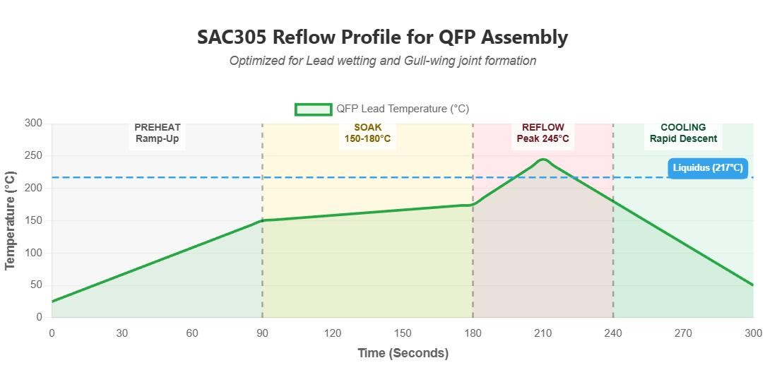
Reflow Profiling (SAC305)
A Lead-Free (SAC305) profile generally has the following zones:
- Preheat: Ramp up at 1–3°C/sec to 150°C.
- Soak: 150–180°C to be maintained for 60–120 seconds. This gives the flux time to activate and eliminates the volatile solvents. It is of high importance for Quad Flat Packages (QFPs) that this step is performed since it guarantees that the whole package body is thermally equilibrated, thus avoiding possible warpage.
- Reflow: Temperature peak of 245°C–250°C. Time Above Liquidus (TAL) should last for 45–75 seconds.
- Cooling: Rapid cooling (<6°C/sec) to achieve a fine-grain solder structure which is advantageous for the strength of joints.
Common QFP Assembly Defects and Troubleshooting
| Defect | Symptom | Root Cause | Solution |
|---|---|---|---|
| Solder Bridging | Connection between adjacent pins | Excessive paste volume or Slumping | Reduce stencil aperture width; Check solder mask dam integrity. |
| Open Joint (Coplanarity) | Pin hovering above the pad | Lead bent upwards (Planarity >0.1mm) | Improved shipping handling (trays vs tubes); Increased paste volume. |
| Solder Balling | Tiny balls near the leads | Paste oxidation or rapid ramp-up | Control moisture; Reduce preheat ramp rate to prevent "explosive" outgassing. |
| Head-in-Pillow (HiP) | Lead sits in paste but doesn't fuse | Warping or oxidized leads | Use N2 (Nitrogen) reflow environment; Check component wettability. |
QFP Component Sourcing and Assembly Reliability Standards
Component Sourcing via JLCPCB
When specifying QFPs for assembly, the source of the component is as vital as the footprint.
- Parts Library Integration: JLCPCB provides access to over 520,000+ in-stock components directly through their Parts Library.
- Basic vs. Extended Parts: "Basic Parts" (such as mainstream STM32 LQFP microcontrollers) are feeders that have been pre-loaded without any additional labor charges. "Extended Parts" are the ones that need feeder loading manually. Where applicable, designers can reduce costs by opting for Basic parts.
Quality Assurance (IPC-A-610)
Final inspection of QFP assemblies is governed by IPC-A-610 Class 2 or Class 3 standards.
- Class 2 (Standard): Most consumer and industrial electronics are allowed under this classification.
- Class 3 (High Reliability): It is the automotive/aerospace criterion. It needs stricter criteria for solder fillet height (at least 50% of lead thickness at the heel).
- Inspection Methods: JLCPCB utilises AOI (Automated Optical Inspection) to detect lead skew and bridging. For QFPs with thermal pads (ePad), X-Ray inspection is used to calculate void percentage (target <25% voiding).
FAQ about Quad Flat Package (QFP)
Q1: Can I route signal traces underneath a QFP body?
Routing of the traces on the top layer under the QFP body is possible, but only if no Exposed Pad (ePad) is present. Should the QFP come with an ePad, top-layer routing under the body is prohibited since it would short to the pad that is grounded. Always make sure that there is enough solder mask covering on vias under the package to avoid solder wicking or shorting.
Q2: What is the preferred packaging for QFP components: Tape & Reel or Trays?
Trays are the overwhelming choice for large QFPs (QFP-100, the final QFP, and higher) etc., as well as for all the variants, fine-pitch among them. The tape packaging sometimes can cause mechanical stress, which leads to bending of the delicate gullwing leads and subsequently the holistic issue of them not being coplanar during assembly. In effect, Trays protect and keep the leads floating "alive," which in turn leads to better placement yield.
Q3: Is it possible to hand-solder or rework a 0.4mm pitch QFP?
While possible for skilled technicians, hand-soldering 0.4mm pitch devices is difficult and prone to bridging. It typically requires a microscope, a "drag soldering" technique with a mini-hoof tip, and a generous application of flux. For consistent reliability, automated SMT assembly (like that offered by JLCPCB) is strongly recommended over hand assembly.
Q4: Why does JLCPCB recommend "Via-in-Pad Plated Over" (VIPPO) for QFPs with ePads?
The traditional open vias are used in the ePad land pattern when thermal vias are inserted in the ePad area, and this can lead to solder being taken away from the main joint through capillary action, thus resulting in voids and poor thermal bonding. VIPPO (or capped vias) overcomes this problem by maintaining a flat plating of the via, which helps to keep the solder paste on the pad, thus ensuring it is available for the thermal interface.
Conclusion: Quad Flat Package (QFP)
The QFP, or Quad Flat Package, is still a vital part of today's electronic devices, providing a flexible option for high-pin-count logic and control applications. But the package's reliability depends entirely on compliance with DFM principles such as land pattern geometry, stencil design, and thermal management.
The JLCPCB's in-stock parts library offers verified supply chain integrity, and advanced SMT capabilities that include X-ray and AOI are some of the features that give engineers the confidence to implement QFP-based designs. The guidelines are applicable whether the project is a new IoT sensor prototype or an industrial controller that is being scaled up, and thus, ensure that the QFP implementation is able to withstand the field's rigorous demands.
Popular Articles
• SMD Diode Code Lookup: Full List, Marking Guide & Identification [2026 Guide]
• SMD Resistor Package Sizes: Complete Size Chart, Footprints & How to Choose
• SMD Capacitor Codes: Identification, Markings, and Polarity
• SMD Capacitor Sizes: Complete Size Chart and Selection Tips for PCB Design and Assembly
• How to Solder SMD Components Like a Pro [2026 Updated]
Keep Learning
PoP Package (Package on Package) Explained: Architecture, Assembly, and SMT Challenges
In the race for miniaturization, fitting more processing power into smaller footprints is the ultimate challenge for PCB designers. Package on Package (PoP) technology answers this by integrating logic and memory vertically, becoming the standard for modern mobile processors. However, this 3D architecture demands advanced SMT assembly capabilities beyond standard fabrication. JLCPCB specializes in the high-precision manufacturing required to master these complex stacks. This guide covers how PoP packa......
What Is a PQFP Package? Plastic Quad Flat Package Design, Footprint, and Assembly Guide
The Plastic Quad Flat Package (PQFP) is a widely used IC package in industrial, automotive, and embedded designs. This article provides a practical, engineering-focused guide to PQFP package. It explains how PQFP is built, when it makes sense to use it, how it compares with newer package types, and what designers should consider in terms of footprint design, thermal performance, signal integrity, manufacturing, and reliability. What Is a PQFP Package (Plastic Quad Flat Package)? A Plastic Quad Flat Pa......
Small Outline Integrated Circuit (SOIC): Package, Specs & Uses
As designs transition from legacy through-hole components to high-density Surface Mount Technology (SMT), the Small Outline Integrated Circuit (SOIC) remains the industry standard for operational amplifiers, flash memory, sensors, and microcontrollers. It stands as a testament to balanced engineering, offering a perfect compromise between the miniaturisation demanded by modern consumer electronics and the ruggedness required for industrial applications. This article serves as a definitive engineering ......
A Complete Guide to Surface Mount Device (SMD)
Imagine holding a smartphone in your hand. Inside that sleek device lies a complex network of thousands of miniature components — resistors smaller than a grain of rice, capacitors thinner than a fingernail, and integrated circuits containing millions of transistors. Without Surface Mount Technology (SMT) and its compact Surface Mount Devices (SMDs), none of this would exist. Just a few decades ago, electronics were bulky. Radios filled desks, computers filled rooms, and assembling a circuit meant dri......
Circuit Breaker Types Explained: MCB, MCCB, RCCB, RCBO, ACB, VCB & SF6 Circuit Breakers
A circuit breaker automatically disconnects power when it detects faults such as overloads or short circuits, protecting equipment and reducing fire risk. Different circuit breaker types are designed for different voltage levels, current ratings, and applications, from household distribution boards to high-voltage substations. This guide explains the most common types - including MCBs, MCCBs, RCCBs, RCBOs, ACBs, VCBs, and SF6 breakers and helps you choose the right one for your application. Figure: Ci......
Quad Flat Package (QFP): The Engineer's Guide to Design, Assembly and Thermal Management
What is QFP Package? The Quad Flat Package (QFP) is one of the most popular surface mount technology (SMT) package formats throughout the history of electronic manufacturing. After it became standard in the 1980s, the QFP has been the industry standard for integrated circuits (ICs) with moderate to high pin counts that typically range from 32 to 304 pins, so it was a good alternative for simple SOIC packages and complex Ball Grid Arrays (BGAs) at the same time. Defined by its "gull-wing" leads extendi......