
The Complete Guide to LED Symbol [2026 Updated]
11 min
- What Is the LED Symbol?
- Understanding the LED Symbol Diagram and Structure
- Types of LED Symbols
- LED Symbol Polarity Explained
- LED Symbol Orientation in Schematics
- How to Read an LED Symbol in a Circuit Step-by-Step
- Common Mistakes When Using LED Symbols
- LED Symbol vs Diode Symbol
- LED Symbol and PCB Design Considerations
- Bring Your LED Circuit to Life with JLCPCB
- FAQs About LED Symbol
- Conclusion
The LED symbol is one of the most widely used electronic symbols in modern circuit design. You will encounter LED symbols in power indicators, microcontroller circuits, and RGB lighting systems.
Whether you are reading a simple circuit diagram or designing a complex multilayer PCB, understanding the LED schematic symbol is essential for reading and designing electronic circuits correctly. This guide covers everything you need to know about the light-emitting diode symbol, from basic anatomy to real-world PCB workflows.
In this guide, you will learn:
- LED symbol diagram and meaning
- Polarity (anode vs cathode)
- LED vs diode vs photodiode
- How to read LED circuits
- Symbol orientation rules
- SMD vs THT LED symbols
- RGB LED symbol basics
- LED package sizes (0402, 0603, 5050)
- From schematic to PCB

Figure: An LED schematic symbol alongside a glowing physical LED on a printed circuit board.
What Is the LED Symbol?
The LED symbol is a diode symbol with two outward arrows representing light emission.
More precisely, it is the schematic representation of a Light Emitting Diode.
It consists of a triangle pointing to a vertical bar (the standard diode shape) with two diagonal arrows added to indicate photon emission.
It is defined under IEC 60617 (latest revision) - the only currently active international standard for graphical schematic symbols.
Note
The former IEEE 315 / ANSI Y32.2 standard defined the exact same graphical representation but was officially inactivated in November 2019 without a replacement.
Always default to IEC 60617 for modern, compliant electronics design.
What the Light Emitting Diode Symbol Represents in a Circuit
The LED circuit symbol is used in schematic diagrams to easily communicate component type, current direction, and optical behavior - all in a single small drawing.
Understanding the LED schematic symbol helps avoid polarity errors during the assembly phase.
| Property | Detail |
|---|---|
| Symbol shape | Diode triangle + vertical cathode bar + two outward arrows |
| Arrow direction | Away from the diode body - indicates light emission |
| Anode (+) | Flat base of the triangle → positive supply |
| Cathode (−) | Vertical bar → ground or negative rail |
| Governing standard | IEC 60617 (latest revision) - live online database, ~1,900 symbols |
| Used in | Schematics, PCB design, EDA libraries, technical documentation |
Electrical Behavior of LED Symbol (Forward and Reverse Bias)
The diode shape (triangle + bar) tells you current flows one way only.
The triangle shows which way current is allowed to travel - always from the flat base toward the bar.
The vertical line is a barrier - current cannot cross it from right to left under normal conditions.
Optical Meaning of LED Symbol (Photon Emission)
An LED consists of a P-type and N-type semiconductor layer joined at a junction. When forward voltage is applied, electrons and holes recombine, releasing energy as photons.
The two arrows tell you this diode also produces light. The arrows show light leaving the component - pointing outward, away from the junction.
Understanding the LED Symbol Diagram and Structure
LED Symbol Diagram Explained (Triangle, Bar, Arrows)
This LED symbol diagram is universally recognized across the electronics industry.
Quick Rule:
- Triangle = current direction
- Bar = cathode
- Arrows = light emission
Three elements make up the LED circuit symbol:
- Triangle (diode body): Points right; represents the PN junction and conventional current direction.
- Vertical bar (cathode): Sits at the triangle tip; represents the potential barrier blocking reverse current.
- Two diagonal arrows: Point away from the symbol at ~45°; represent photon emission.
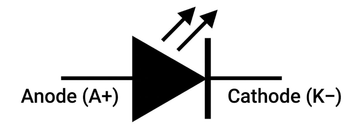
Figure: Standard LED schematic symbol with labeled anode, cathode, diode body, and light emission arrows.
Why LED Symbol Has Arrows (Light Emission Explanation)
Quick Rule:
- Arrows pointing away = LED (emitting light)
- Arrows pointing inward = Photodiode (receiving light)
- No arrows = Standard rectifier diode
A standard silicon diode dissipates energy as heat - invisible, and irrelevant to the schematic reader. An LED converts that same junction energy into photons.
The arrows make this visible without any additional labels. To understand foundational diode mechanics further, you can review this comprehensive diode symbol guide.
The arrows mean: energy is leaving this junction as light, not as heat. They do not indicate current direction (the triangle handles that).
They indicate radiation direction: outward from the source. This is why the arrows are the single most important visual feature for identifying an LED in a complex schematic.
Types of LED Symbols
The core symbol remains identical across various LED types; specific designations are carried in labels, the Bill of Materials (BOM), and PCB footprints.
Standard LED Symbol
Used for visible indicators (red, green, blue, white, etc.). The specific color is annotated in the BOM or next to the component reference (e.g., D1 RED).
Infrared LED Symbol
Visually identical to the standard symbol. The "IR" designation appears in the component label (e.g., D3 IR) and the BOM wavelength column.
RGB LED Symbol
Represents three LEDs combined into one schematic block. They typically share a single common terminal.
The RGB LED symbol is commonly used in microcontroller and lighting circuits.
| Variant | Common Terminal | Channel Control |
|---|---|---|
| Common cathode | All cathodes → GND | Apply voltage to each anode (R, G, B) to activate |
| Common anode | All anodes → VCC | Pull each cathode to GND to activate |
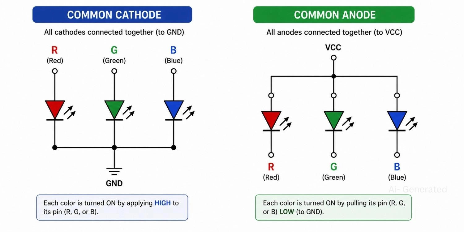
Figure: Schematic diagram comparing common cathode and common anode RGB LED wiring configurations.
SMD LED Symbol vs Through-Hole LED Symbol
The schematic symbol does not change with package type. A 0603 SMD LED uses the exact same triangular circuit symbol as a chunky 5mm Through-Hole LED.
LED Symbol Polarity Explained
Polarity is where the most damaging circuit errors occur. The symbol encodes polarity directly - no guessing required.
How to Identify Anode and Cathode in LED Symbol
Memory anchor: the triangle always "points from +" to "−".
The flat base of the triangle is your positive intake, and the vertical line represents where the current exits.
LED Symbol Polarity Rule
Quick Polarity Rule:
- Flat base of triangle = Anode (+) → connect to positive supply
- Vertical bar = Cathode (−) → connect to ground
- Triangle points in the direction of conventional current flow.
LED Polarity in Physical Components (SMD vs Through-Hole)
| Physical LED Type | Anode Marker | Cathode Marker |
|---|---|---|
| Through-hole (5mm, 3mm) | Longer lead | Shorter lead |
| Through-hole body | - | Flat edge on plastic case |
| SMD (0402, 0603) | Refer to datasheet | Dot, line, or notch - varies by manufacturer |
| SMD (5050 RGB) | Refer to datasheet | Pin 1 per package marking |
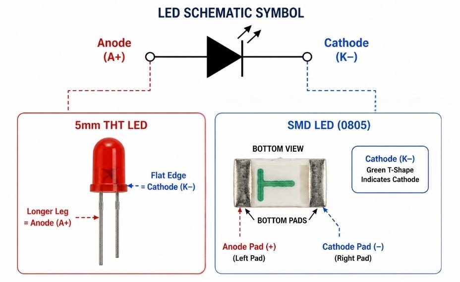
Figure: The anode and cathode of an LED schematic symbol to physical markers on a through-hole and SMD LED.
What happens if the LED Is Connected in Reverse
What actually happens when an LED is installed backwards:
- Reverse voltage below PIV: LED stays dark; no current flows; no immediate damage.
- Reverse voltage near PIV: Small leakage current begins; junction heats slightly.
- Reverse voltage exceeding PIV: Junction breaks down permanently; the LED may short the supply rail in failure mode.
Most indicator LEDs have a Peak Inverse Voltage (PIV) of only 5–10V - easily exceeded in common 5V or 12V circuits if the polarity is wrong.
For a deeper dive into physical component orientation and troubleshooting, refer to our comprehensive LED polarity guide.
LED Symbol Orientation in Schematics
LED Symbol Orientation Left to Right vs Vertical
The LED symbol orientation does not affect circuit function, but professional conventions exist for readability:
- Horizontal (left-to-right): Most common - current flows left to right across the schematic.
- Vertical (top-to-bottom): Often used in power rail layouts - matches the downward current flow convention from VCC to GND.
Flipped LED Symbol Direction in Circuit Diagrams
- Flipped (right-to-left): Electrically allowed, but you must ensure polarity remains unambiguous from net labels. This orientation is generally discouraged as it breaks reading flow.
Best Practices for LED Symbol Orientation in Schematics
Consistent orientation throughout your schematic prevents tracing confusion. Always align LEDs so current visually flows in the same direction as the rest of the schematic's logic.
How to Read an LED Symbol in a Circuit Step-by-Step
Learning how to read an LED symbol circuit correctly ensures your components won't burn out upon powering up.
How to Identify Current Flow in LED Circuits
- Locate the anode (flat base of triangle) and trace it to the positive supply.
- Locate the cathode (vertical bar) and trace it to ground.
Where to Place Resistor in LED Circuit
- Find the series resistor: Understanding the resistor symbol and its placement is crucial. Physically, it can safely be placed before the anode or after the cathode, as the current-limiting effect is identical in series.
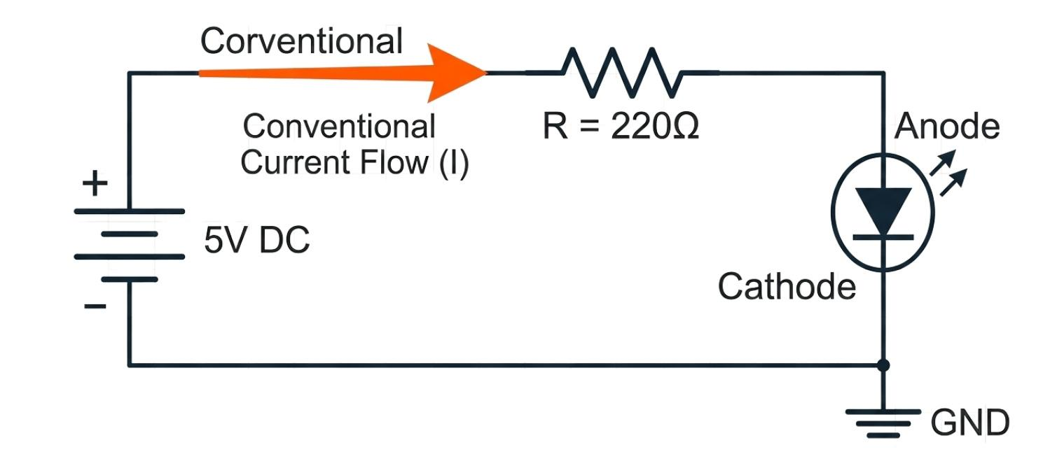
Figure: A basic schematic diagram showing a 5V power source, a current-limiting resistor, and an LED connected in series.
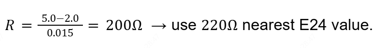
LED Resistor Calculation Formula and Example
- Calculate resistor value using Ohm's Law to prevent diode destruction.
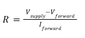
Example: 5V supply, red LED (Vf = 2.0V), target current 15mA.
Common Mistakes When Using LED Symbols
1. Confusing LED Symbol with Photodiode Symbol
While their symbols are almost identical (differing only by arrow direction), mixing them up is a severe documentation error.
Advanced EDA tools may flag a Design Rule Check (DRC) error, and it can mislead assembly engineers into sourcing an optical receiver instead of a light emitter.
2. Misinterpreting LED Symbol Arrows
A common novice mistake is assuming the arrows represent electrical current leaving the circuit. The arrows strictly denote the emission of light (photons).
3. Incorrect LED Polarity in Circuit Design
Accidentally swapping the anode and cathode in the schematic will result in a backwards footprint on the PCB. The LED will be reversed-biased, blocking current and failing to illuminate.
LED Symbol vs Diode Symbol
| Feature | Standard Diode | LED |
|---|---|---|
| Triangle + cathode bar | ✓ | ✓ |
| Outward emission arrows | ✗ | ✓ |
| One-way conduction | ✓ | ✓ |
| Emits visible / IR light | ✗ | ✓ |
| Typical forward voltage | 0.6–0.7 V (Silicon) | 1.8–3.5 V |
| Forward current (indicator) | Up to several amps | 5–30 mA |
| Primary use | Rectification, protection | Indication, illumination |
Why LED Symbol Includes Arrows but Diode Does Not
The sole visual difference is two arrows. In a dense schematic, this is easy to miss under time pressure, which is precisely why IEC 60617 requires those arrows to be drawn distinctly and not implied.
Standard diodes dissipate power safely as heat, but LEDs are explicitly designed to emit photons, which is visually categorized by the arrows.
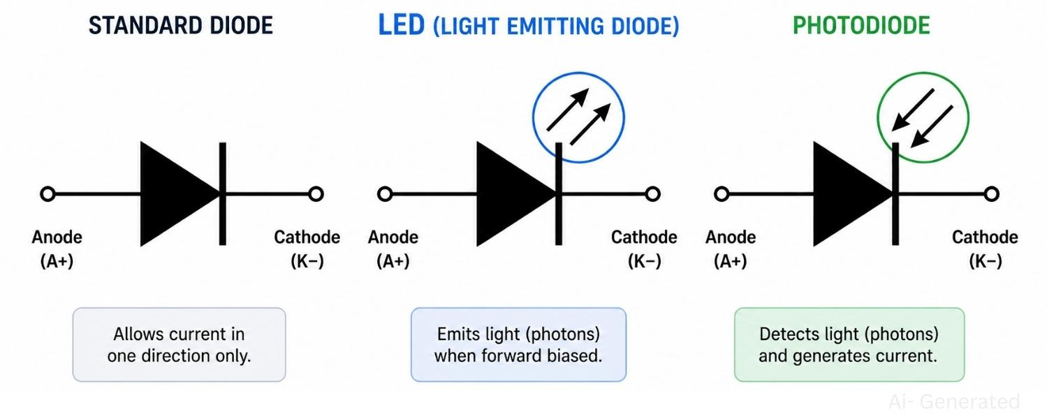
Figure: Comparison of rectifier diode, LED, and photodiode schematic symbols showing arrow direction differences.
LED Symbol and PCB Design Considerations
Transitioning from a schematic diagram to a physical board requires precise engineering and seamless PCB assembly.
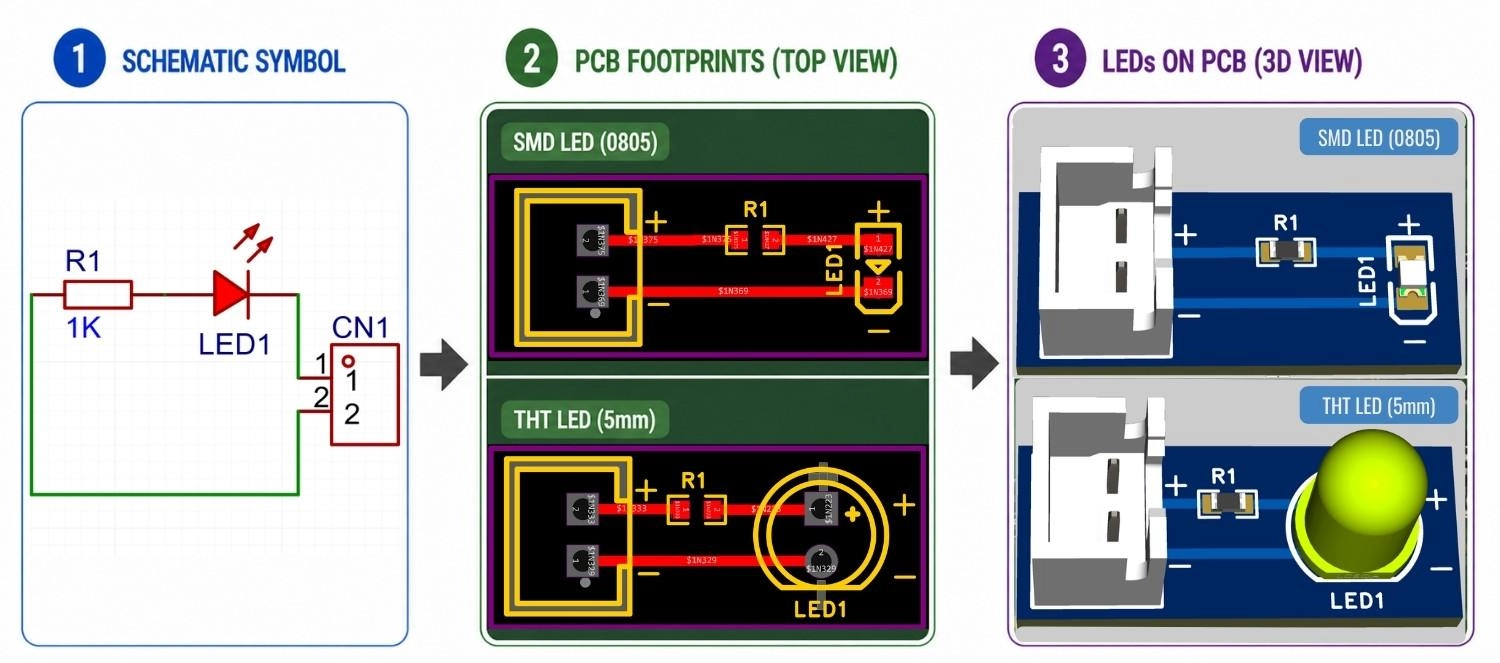
Figure: Three-stage workflow showing an LED schematic symbol, its corresponding PCB footprints, and the final 3D rendered SMD and through-hole LEDs on a PCB.
LED Symbol vs PCB Footprint Difference
| Design Layer | What It Represents |
|---|---|
| Schematic | LED symbol with net connections (anode net, cathode net). |
| PCB footprint | Physical pad size, spacing, orientation anchor. |
Mapping LED Anode and Cathode in PCB Layout
| Design Layer | What It Represents |
|---|---|
| Silkscreen layer | Component outline + polarity marker on the board. |
| Assembly drawing | Pick-and-place orientation reference. |
From LED Schematic Symbol to PCB Assembly
When designing in EDA tools like EasyEDA or KiCad, you can easily source standard surface mount components directly from the JLCPCB Parts library to ensure your schematic footprint perfectly matches the physical hardware during the reflow soldering process.
Bring Your LED Circuit to Life with JLCPCB
The LED symbol is a critical instruction set for your electronics design workflow. By understanding its visual elements, you eliminate guesswork and prevent costly errors, ensuring your schematic perfectly aligns with your physical hardware.
Ideal for:
- Indicator LED circuits
- RGB lighting modules
- Embedded system designs
Ready for production? JLCPCB bridges the gap from design to finished boards with fast, reliable PCB assembly.
FAQs About LED Symbol
Q: Can the LED symbol represent laser diodes (LDs)?
No. Laser diodes use a distinct IEC 60617 symbol and are explicitly labeled LD. Using a standard LED symbol misrepresents the component's emission characteristics.
Q: Why do some LED circuits show no resistor in the schematic?
Current limiting may be handled internally by an LED module, a constant-current LED driver IC, or a precisely rated microcontroller pin.
Q: How do I confirm LED polarity on a bare board?
Use a multimeter in diode mode. Place the red probe on the suspected anode and black on the cathode. A forward voltage reading confirms orientation; "OL" (overload) means it is reversed.
Q: Does the LED symbol change if I use a higher voltage circuit?
No. The symbol represents the component type, not its voltage rating. You just need to recalculate your series current-limiting resistor for the higher supply voltage.
Q: Why do my LED pins mismatch between the schematic symbol and PCB footprint?
This happens when EDA libraries use different naming conventions (e.g., 'A' and 'K' vs. '1' and '2'). Always verify pin mapping in your software to avoid Design Rule Check (DRC) errors or reversed footprints.
Conclusion
The LED symbol is a critical instruction set for your electronics design workflow. By understanding its visual elements, the diode triangle, cathode bar, and outward arrows, you eliminate guesswork and prevent costly errors, ensuring your schematic perfectly aligns with your physical hardware.
Popular Articles
• How to Create a Bluetooth-Controlled Car With Arduino: A Step-by-Step Guide
• How to Design and Assemble a Reliable ESP32 Module PCB on a 2-Layer Board
• The Ultimate Guide to Relay Symbol: Coil, Contacts, Diagrams, and Circuit Applications
• How to Identify SMD LED Polarity: Markings, Testing, and PCB Tips
• The Ultimate Guide to PCBA: Process,Types and Techniques for the Electronics Enthusiast
Keep Learning
How to Design an ESP32-S3 Development Board from Scratch: A 4-Layer PCB Design Tutorial
Designing your own ESP32-S3 development board gives you complete control over your hardware architecture while preparing your IoT projects for commercial production. Instead of relying on bulkier, off-the-shelf boards, building a custom design allows you to optimize the board space, expose only the required GPIO pins, and integrate peripherals directly onto a single substrate. In this tutorial, we will design a 4-layer ESP32-S3 development board from scratch. We will walk through the entire hardware d......
Arduino LED Driver Tutorial: Control More LEDs with 74HC595 and MAX7219
Arduino GPIO pins run out quickly in larger LED projects. By utilizing dedicated LED drivers and expansion ICs, you can drastically reduce pin usage, eliminate processor-heavy multiplexing loops, and simplify display wiring. In this guide, you will learn the operational architecture, wiring configurations, cascading techniques, and optimization strategies for the 74HC595 shift register and the MAX7219 LED driver. Why Arduino Projects Need LED Driver ICs Arduino GPIO and Current Limitations An ATmega32......
How to Create a Bluetooth-Controlled Car With Arduino: A Step-by-Step Guide
This tutorial walks through the complete engineering and implementation of a two-wheel Bluetooth RC car with an Arduino Nano module on a specially designed PCBA (Printed Circuit Board Assembly). While many hobbyists start by wiring motors and Bluetooth modules with jumper cables on a breadboard, this approach is prone to disconnection and signal noise. This guide upgrades that process by teaching you how to design a professional mainboard. Key Design Features Controller: Arduino Nano used as a plug-in......
Fiducial Marks in PCB and SMT Assembly: A Complete Guide to Accuracy and Design Rules
Modern Printed Circuit Boards (PCBs) are complex, integrating high-density components like 0.4mm pitch Ball Grid Arrays (BGAs), 0201 passives, and fine-pitch Quad Flat No-Lead (QFN) packages. In this advanced manufacturing environment, achieving placement accuracy measured in micrometers is crucial. A significant challenge in automated manufacturing is how pick-and-place machines, which handle thousands of components per hour, precisely locate the PCB. A board on a conveyor system is never in the perf......
Alternating Current vs Direct Current (AC vs DC): What's the Difference?
Electric current flows in two primary forms: alternating current (AC) and direct current (DC). AC periodically reverses direction, while DC flows steadily in one direction. AC powers the industrial and residential electrical grids, while DC powers batteries, electric vehicles, and nearly all modern consumer electronics. Understanding the core differences between AC and DC matters when designing power supplies, selecting electronic components, or laying out printed circuit boards (PCBs). This guide com......
Arduino LED Multiplexing Tutorial: Control More LEDs with Fewer Pins
The Arduino Uno is a powerful tool for prototyping, but driving multiple LEDs directly quickly exhausts its 20 GPIO pins and its 200 mA absolute maximum package current limit. To bypass these hardware bottlenecks, engineers and hobbyists use LED multiplexing to scale display outputs efficiently without upgrading the microcontroller. In this guide, you will learn the core principles of LED matrix scanning, Charlieplexing, refresh timing, ghosting fixes, and practical Arduino code without relying on any......