
SMD Transistor Code Lookup: Identify Markings, Pinout & Multimeter Test Guide
14 min
- How to Identify an SMD Transistor Instantly
- Instant SMD Transistor Code Lookup Table
- What is an SMD Transistor Code?
- How to Identify SMD Transistor Type: BJT vs MOSFET Comparison
- SMD Transistor Package Types and Pinout Guide
- How to Identify Unknown SMD Transistor [Step-by-Step Guide]
- How to Test an SMD Transistor Using a Multimeter [Step-by-Step Guide]
- Why SMD Transistor Codes Are Not Standardized
- Common SMD Transistor Code Confusion Problems
- Common SMD Transistor Replacement Mistakes (Repair Guide)
- How to Choose a Safe SMD Transistor Replacement
- Real PCB Repair Case: Burnt SMD Transistor(MOSFET) Failure Analysis
- FAQ about SMD Transistor Code
- Conclusion
Repairing a circuit board often brings a familiar frustration: staring at a tiny, three-legged black component with an obscure two- or three-letter code. Whether troubleshooting a bare prototype or a mass-produced PCBA, knowing how to quickly decode these surface-mount device (SMD) markings is an essential skill for any electronics engineer or repair technician.
In this comprehensive guide, you will learn:
How to Identify an SMD Transistor Instantly
If you need to identify an unknown SMD transistor code right now, follow this rapid identification workflow:
- Read the top marking code: Note the exact alphanumeric characters (e.g., "J3Y" or "1AM"). Look for microscopic dots indicating manufacturer or lead-free status.
- Identify the package: Determine if the footprint is SOT-23, SOT-89, or SOT-223 using digital calipers.
- Trace the circuit: Is it driving a relay, regulating power, or switching a digital signal? This hints at its function.
- Find the pin configuration: Cross-reference the package type with standard pinout diagrams to locate the Base/Gate, Collector/Drain, and Emitter/Source.
- Test with a multimeter: Perform a diode test across the pins to confirm whether it is an NPN, PNP, N-Channel, or P-Channel device.
Instant SMD Transistor Code Lookup Table
Below is a quick reference chart for the most frequently encountered SMD transistor codes. Use this lookup to jumpstart your repair process and identify standard replacement parts.
SMD Code | Part Number | Type | Package | Pinout (1-2-3) |
|---|---|---|---|---|
1AM | MMBT3904 | NPN BJT | SOT-23 | Base - Emitter - Collector |
2A | MMBT3906 | PNP BJT | SOT-23 | Base - Emitter - Collector |
2TY | S8550 | PNP BJT | SOT-23 | Base - Emitter - Collector |
J3Y | S8050 | NPN BJT | SOT-23 | Base - Emitter - Collector |
K72 | 2N7002 | N-Ch MOSFET | SOT-23 | Gate - Source - Drain |
A79T | AO3407 | P-Ch MOSFET | SOT-23 | Gate - Source - Drain |
M6 | S9015 | PNP BJT | SOT-23 | Base - Emitter - Collector |
1F | BC847B | NPN BJT | SOT-23 | Base - Emitter - Collector |
L6 | 2SC1623 | NPN BJT | SOT-23 | Base - Emitter - Collector |
W1 | PMBT3904 | NPN BJT | SOT-23 | Base - Emitter - Collector |
6C | BC817 | NPN BJT | SOT-23 | Base - Emitter - Collector |
Y1 | S9014 | NPN BJT | SOT-23 | Base - Emitter - Collector |
L2 | BC807 | PNP BJT | SOT-23 | Base - Emitter - Collector |
What is an SMD Transistor Code?
An SMD transistor code is a shortened identification string laser-etched onto the top plastic casing of a surface-mount transistor.
Why Marking Codes Exist
Because modern electronics demand extreme miniaturization, standard surface-mount packages simply lack the physical space to print full, legacy part numbers like "MMBT3904" or "2N2222". Instead, manufacturers condense the identification into two to four characters.
Why Codes Are Confusing
These shortened codes are not universal. A single code like "1A" can represent entirely different components depending on the manufacturer and the year of production. This makes reverse-engineering a circuit highly dependent on context and proper testing.
Manufacturer Specific Lookup Systems
Because the system is heavily manufacturer-specific, decoding these markings requires cross-referencing datasheets or specialized marking databases. This is a very similar process to reading SMD resistor codes or identifying capacitor polarity.
How to Identify SMD Transistor Type: BJT vs MOSFET Comparison
Before attempting a replacement, you must determine whether the component is a Bipolar Junction Transistor (BJT) or a Metal-Oxide-Semiconductor Field-Effect Transistor (MOSFET). Mistaking one for the other is a fast track to circuit failure.
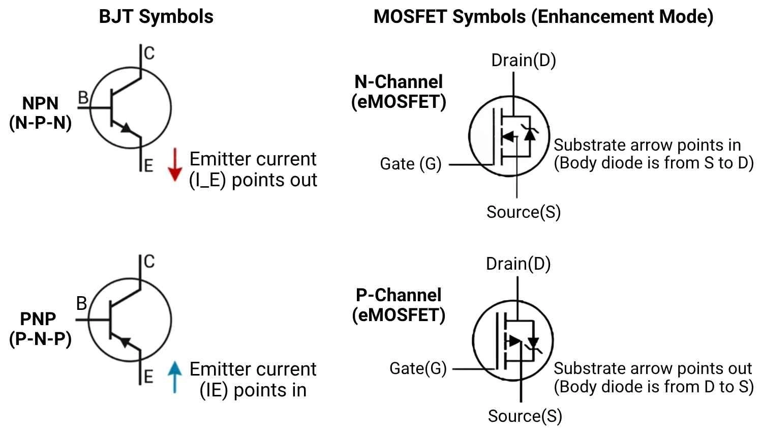
Figure: Schematic symbol comparison showing the structural and polarity differences between NPN/PNP BJTs and N-Channel/P-Channel MOSFETs.
Key Electrical Differences between BJT and MOSFET
Parameter | BJT (Bipolar Junction Transistor) | MOSFET (Metal-Oxide-Semiconductor) |
|---|---|---|
Control Method | Current-controlled | Voltage-controlled |
Pin Designations | Base (B), Emitter (E), Collector (C) | Gate (G), Drain (D), Source (S) |
Forward Drop | Present (~0.6V to 0.7V) | Extremely low (dependent on Rds-on) |
Body Diode | Not present | Present (between Source and Drain) |
Typical Application | Amplification, low-current switching | High-current power switching |
How to Identify BJT vs MOSFET Using a Multimeter Quickly
To quickly tell them apart on your workbench:
- BJT shows two distinct PN junction voltage drops when probed from the Base.
- MOSFET shows a single body diode drop (between Source and Drain) only.
- MOSFET gate is insulated, meaning it will show infinite resistance/open loop to the other pins.
SMD Transistor Package Types and Pinout Guide
Recognizing the physical package type is just as important as reading the code. Correctly identifying standard SOT pinouts is crucial, especially when moving a prototype to a PCB Assembly run where incorrect footprint mapping ruins the entire production batch.
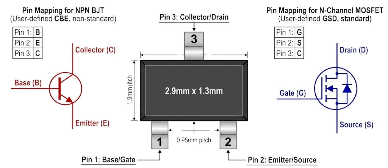
Figure: SOT-23 transistor pinout diagram showing standard mapping of both BJT and MOSFET.
Package Type | Dimensions (L x W) | Typical Power Dissipation | Typical Use Case |
|---|---|---|---|
SOT-23 | 2.9 mm × 1.3 mm | ~250 mW to 350 mW | Signal switching, logic translation |
SOT-89 | 4.5 mm × 2.5 mm | ~500 mW to 1 W | Medium power audio, LED driving |
SOT-223 | 6.5 mm × 3.5 mm | ~1 W to 1.5 W | Linear regulators, power switching |
SOT-23 Transistor Package
The most ubiquitous small-signal transistor package. Almost always features a standard 1-Base, 2-Emitter, 3-Collector pinout.
SOT-89 Transistor Package
Features a large center thermal pad (usually the Collector/Drain) designed to sink heat directly into the PCB copper.
SOT-223 Transistor Package
A larger power package used for higher current applications, easily identifiable by its large top-side thermal tab.
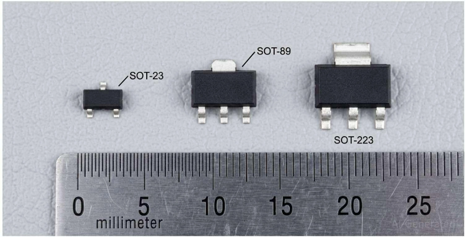
Figure: Physical size comparison of SOT-23, SOT-89, and SOT-223 SMD transistor packages.
How to Identify Unknown SMD Transistor [Step-by-Step Guide]
When faced with a completely unknown SMD component, use this systematic approach to deduce its identity:
Step 1. Visual Inspection
Clean the component with isopropyl alcohol and use a jeweler's loupe or microscope to read the code clearly. Watch out for dots or underscores.

Figure: Using a digital microscope to read a tiny SMD transistor marking code on a circuit board.
Step 2. Circuit Tracing
Follow the PCB traces connected to the component to understand its role. Contextual Identification Clues:
- Near MCU: Likely a small-signal switching transistor translating logic levels.
- Near Inductor / Power Input: Highly likely to be a power MOSFET used for voltage regulation.
- Near Relay / Motor: Likely a driver transistor designed to handle inductive loads.
Step 3. Pin Mapping
Use a continuity tester to determine which pin connects to Ground, VCC, or a microcontroller I/O pin. For example, if Pin 2 connects straight to Ground, it is likely an N-Channel MOSFET Source or NPN Emitter.
Step 4. Multimeter Verification
Probe the component out of the circuit to map its internal junctions and confirm the exact polarity.
How to Test an SMD Transistor Using a Multimeter [Step-by-Step Guide]
Electrical verification is required to know if the part is actually functional. Set your digital multimeter (DMM) to "Diode Test" mode.

Figure: Testing an SMD transistor out of circuit using a digital multimeter in diode mode.
BJT Testing Steps (NPN Example):
MOSFET Testing Steps (N-Channel Example):
Multimeter Reading (Diode Mode) | Meaning / Component Status |
|---|---|
0.5V - 0.7V (One direction) | Normal PN junction (Healthy BJT) |
0.00V / Beep | Short circuit (Dead transistor) |
"OL" or Infinite (Both directions) | Open circuit (Blown internal bond wire) |
0.4V - 0.6V (Source to Drain) | Normal MOSFET body diode |
Table: A reference table showing multimeter diode mode readings and their corresponding component health status.
In-Circuit vs Out-of-Circuit Testing for Transistors
Always try to test transistors out of the circuit. In-circuit parallel components (like bypass resistors or low-impedance inductors) will spoof your multimeter readings and falsely indicate shorts. Use proper soldering techniques to remove the part safely.
Why SMD Transistor Codes Are Not Standardized
You might wonder why there isn't a singular, universal database. The lack of standardization stems from three main factors:
- Manufacturer Internal Tables: Every semiconductor fab utilizes its own internal tracking system to label parts.
- Package Size Limits: A tiny 2.9mm part simply cannot fit standard naming conventions like JEDEC's full part strings.
- Batch Codes: Often, extra characters in a code signify the manufacturing plant, date code, or specific silicon batch.
Common SMD Transistor Code Confusion Problems
Because codes are short, overlaps are inevitable. A common transistor replacement mistake is assuming a two-letter code only belongs to one specific part.
SMD Code | Possible Parts | Risk of Confusion |
|---|---|---|
A1 | MMBT3904 (NPN BJT) / BAW56 (Dual Diode) | Component type confusion (Diode vs BJT) resulting in immediate circuit failure |
J3Y | S8050 / BC847 | Current rating issue (S8050 handles up to 500mA, BC847 only 100mA) |
2A | MMBT3906 (PNP BJT) / MM3Z9V1 (Zener Diode) | Polarity and component type confusion resulting in dead shorts |
Common SMD Transistor Replacement Mistakes (Repair Guide)
When repairing a circuit board, misidentifying a component can lead to catastrophic downstream failures. Avoid these common pitfalls:
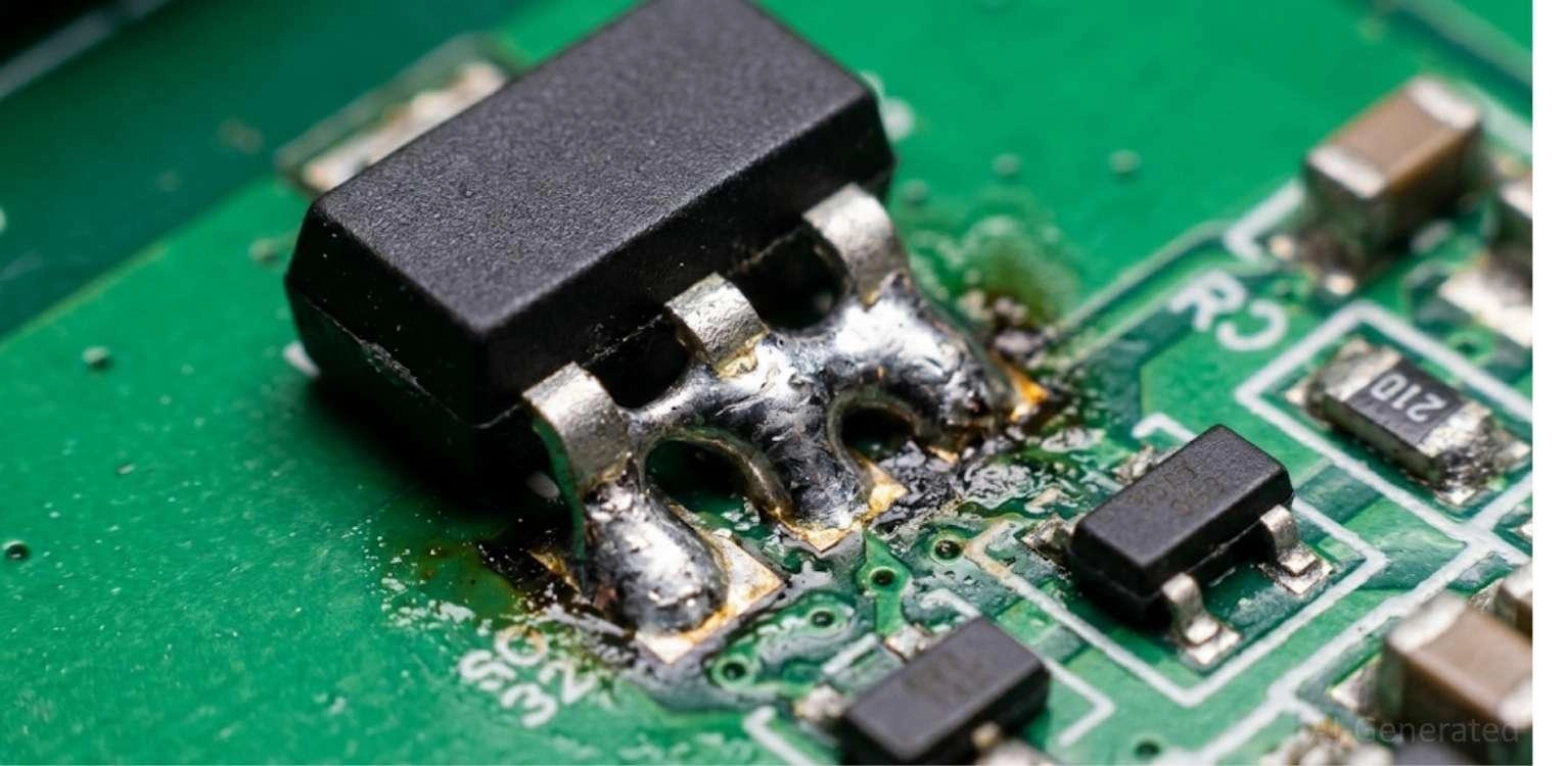
Figure: Solder bridging caused by forcing an incorrect transistor package size onto a PCB footprint.
- Wrong Polarity: Installing a PNP where an NPN is required will immediately block circuit operation and potentially short the power rail.
- Wrong Package Size: Squeezing a SOT-23 into a smaller SOT-323 footprint almost guarantees solder bridging.
- MOSFET Replaced with BJT: Replacing a voltage-controlled MOSFET with a current-driven BJT will result in circuit malfunction because BJTs require continuous base current.
- Upside-Down Reading: Reading "M1" as "1W" will completely derail your datasheet search and lead to buying the wrong part.
- Underrated Current Device: Swapping a 500mA transistor with a 100mA lookalike will cause immediate thermal runaway under load.
How to Choose a Safe SMD Transistor Replacement
When a direct replacement is unavailable, you must substitute it carefully. Accessing a high-quality parts library is essential. Use this checklist to ensure a safe component swap:
- Match Polarity: NPN must replace NPN; N-Channel must replace N-Channel.
- Match Voltage (Vce/Vds): The replacement must handle a maximum breakdown voltage equal to or greater than the original.
- Match Current (Ic / Id): The new part must sustain equal or greater continuous current.
- Match Gain (hFE): For BJTs, ensure the DC gain is similar, especially in sensitive analog circuits.
- Match Rds(on) & Vgs(th): For MOSFETs, a higher Rds(on) will cause the new MOSFET to overheat under the same load. Ensure the gate threshold triggers correctly at your circuit's logic level.
Real PCB Repair Case: Burnt SMD Transistor(MOSFET) Failure Analysis
Consider this field failure case study that highlights the importance of correct SMD component identification.
Situation: A drone motor controller fails mid-flight. Upon opening the casing, you are hit with the distinct, acrid smell of burnt epoxy. Visual inspection reveals a scorched SOT-23 transistor near the motor driver IC.
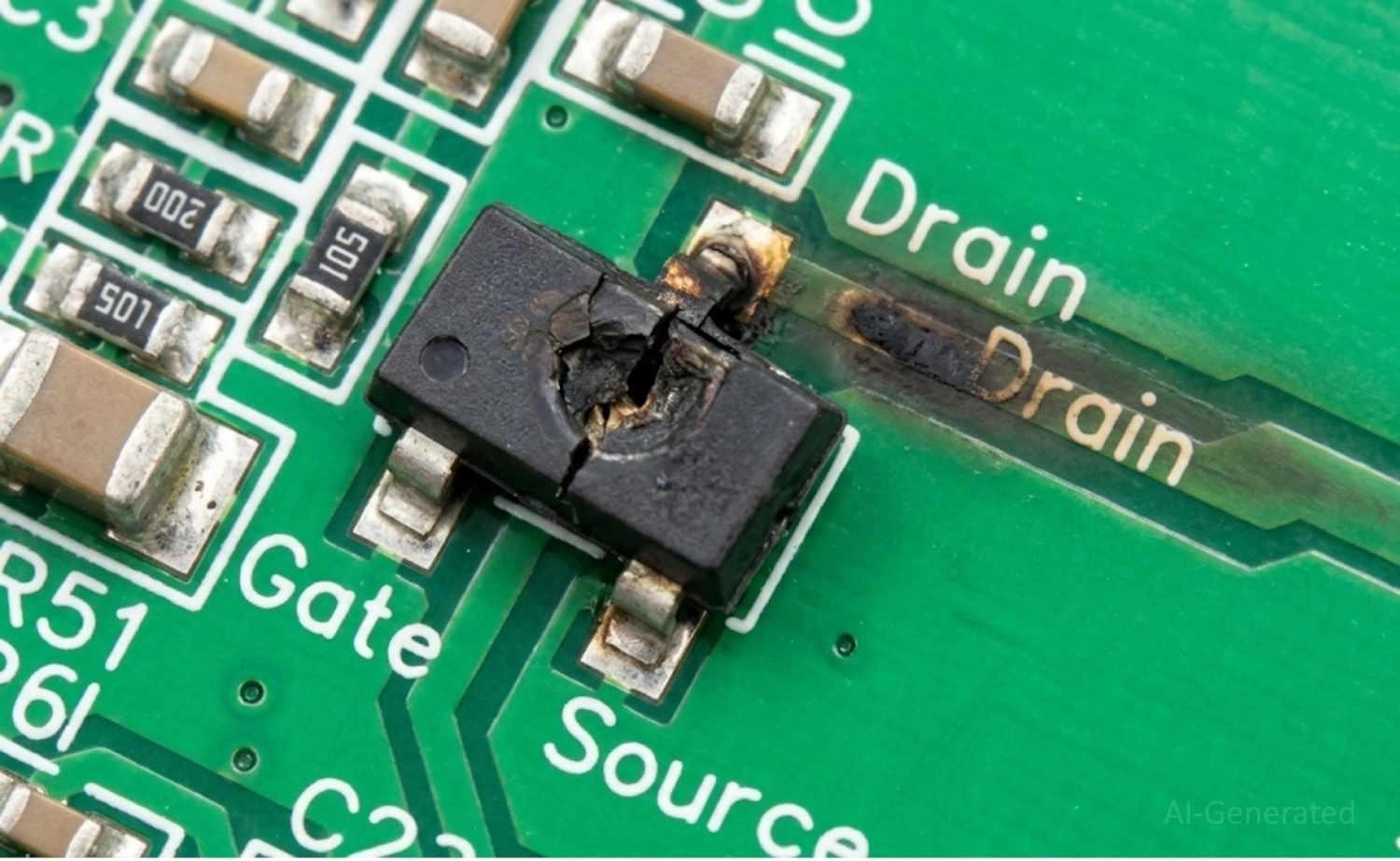
Figure: Burnt SOT-23 SMD transistor showing severe thermal damage on a printed circuit board.
Diagnosis: The marking was heavily charred and resembled "A2" (which often denotes a common diode or low-power BJT). However, tracing the circuit revealed the middle pin connected directly to the motor (a high-current inductive load) and another pin connected to ground, indicating the need for a power switching device.
Root Cause: A previous technician had installed an undersized, incorrectly coded BJT (likely rated for only 800 mA) instead of the required power MOSFET needed to handle the 3–5 A peak motor current.
Failure Mechanism: The incorrectly installed BJT could not withstand the inductive voltage spikes generated by the motor load. Inductive kickback during PWM switching likely caused voltage spikes that exceeded the transistor’s Safe Operating Area (SOA), leading to catastrophic overheating.
Failure symptoms included:
- Intermittent motor startup
- Rapid thermal rise
- Eventual short-circuit failure
- Severe PCB pad discoloration and delamination
Correct MOSFET Replacement & PCB Restoration: Using a robust marking database and the circuit context, the original part was deduced to be an SI2302 N-Channel MOSFET. A matching replacement was sourced, the MCU gate logic was verified as intact, and the new component was soldered, fully restoring the drone.
If this were part of a larger, recurring failure in a custom design, this would be the perfect time to optimize your schematic and get a quick quote for an updated, more robust PCB revision.
FAQ about SMD Transistor Code
Q: Can a transistor marking be fake?
Yes. In the gray market of electronic components, counterfeiters often remark cheap, low-spec transistors with the codes of high-performance parts. Always source components from reputable distributors or a verified parts library to avoid premature circuit failure.
Q: Can an SMD transistor work if it is partially damaged?
Rarely. BJTs generally fail completely - either shorting internally or burning open. However, a MOSFET with a degraded gate oxide might "partially" turn on, resulting in massive heat generation and highly erratic circuit behavior before total failure.
Q: How do I identify a digital transistor marking?
Digital transistors (pre-biased transistors) look exactly like standard BJTs but contain internal series and base-emitter resistors. Multimeter diode tests will yield strange, high-resistance readings. Always verify the marking code against a datasheet to confirm if it contains internal bias resistors.
Q: Can a MOSFET replace a BJT?
In some very specific logic-level switching scenarios, yes, but generally no. They operate on entirely different principles (voltage control vs. current control). Direct swapping without modifying the surrounding bias circuitry will usually fail.
Q: Why does a transistor overheat immediately after replacement?
If a replacement transistor overheats instantly, it is either the wrong part (e.g., higher Rds-on than the original), installed backward, or the underlying circuit fault that destroyed the first transistor (such as a shorted inductive load or bad driver IC) has not been resolved.
Q: Can marking codes fade due to heat?
Yes. Excessive thermal stress can cause the epoxy casing of the transistor to degrade and discolor, obscuring or completely burning away the laser-etched markings. In these cases, identification is strictly dependent on circuit reverse-engineering.
Q: Can I use a higher current transistor as a replacement?
Usually, yes. Replacing a 100mA transistor with a 500mA transistor of the same type and polarity is generally safe and may even improve reliability, provided the package fits the PCB footprint, and the switching speed characteristics remain compatible with the circuit.
Conclusion
Mastering SMD transistor identification transforms PCB repair from a frustrating guessing game into an exact engineering science. By combining visual marking lookups, footprint identification, and rigorous multimeter testing, you can confidently decode, test, and replace unknown components. Whether you are repairing legacy consumer electronics or prototyping hardware for mass production, understanding these surface mount devices builds deep engineering confidence.
Keep this guide bookmarked - you will need it every time you repair a PCB.
Popular Articles
• SMD Diode Code Lookup: Full List, Marking Guide & Identification [2026 Guide]
• SMD Resistor Package Sizes: Complete Size Chart, Footprints & How to Choose
• SMD Capacitor Codes: Identification, Markings, and Polarity
• SMD Capacitor Sizes: Complete Size Chart and Selection Tips for PCB Design and Assembly
• How to Solder SMD Components Like a Pro [2026 Updated]
Keep Learning
PoP Package (Package on Package) Explained: Architecture, Assembly, and SMT Challenges
In the race for miniaturization, fitting more processing power into smaller footprints is the ultimate challenge for PCB designers. Package on Package (PoP) technology answers this by integrating logic and memory vertically, becoming the standard for modern mobile processors. However, this 3D architecture demands advanced SMT assembly capabilities beyond standard fabrication. JLCPCB specializes in the high-precision manufacturing required to master these complex stacks. This guide covers how PoP packa......
What Is a PQFP Package? Plastic Quad Flat Package Design, Footprint, and Assembly Guide
The Plastic Quad Flat Package (PQFP) is a widely used IC package in industrial, automotive, and embedded designs. This article provides a practical, engineering-focused guide to PQFP package. It explains how PQFP is built, when it makes sense to use it, how it compares with newer package types, and what designers should consider in terms of footprint design, thermal performance, signal integrity, manufacturing, and reliability. What Is a PQFP Package (Plastic Quad Flat Package)? A Plastic Quad Flat Pa......
Small Outline Integrated Circuit (SOIC): Package, Specs & Uses
As designs transition from legacy through-hole components to high-density Surface Mount Technology (SMT), the Small Outline Integrated Circuit (SOIC) remains the industry standard for operational amplifiers, flash memory, sensors, and microcontrollers. It stands as a testament to balanced engineering, offering a perfect compromise between the miniaturisation demanded by modern consumer electronics and the ruggedness required for industrial applications. This article serves as a definitive engineering ......
A Complete Guide to Surface Mount Device (SMD)
Imagine holding a smartphone in your hand. Inside that sleek device lies a complex network of thousands of miniature components — resistors smaller than a grain of rice, capacitors thinner than a fingernail, and integrated circuits containing millions of transistors. Without Surface Mount Technology (SMT) and its compact Surface Mount Devices (SMDs), none of this would exist. Just a few decades ago, electronics were bulky. Radios filled desks, computers filled rooms, and assembling a circuit meant dri......
Circuit Breaker Types Explained: MCB, MCCB, RCCB, RCBO, ACB, VCB & SF6 Circuit Breakers
A circuit breaker automatically disconnects power when it detects faults such as overloads or short circuits, protecting equipment and reducing fire risk. Different circuit breaker types are designed for different voltage levels, current ratings, and applications, from household distribution boards to high-voltage substations. This guide explains the most common types - including MCBs, MCCBs, RCCBs, RCBOs, ACBs, VCBs, and SF6 breakers and helps you choose the right one for your application. Figure: Ci......
Quad Flat Package (QFP): The Engineer's Guide to Design, Assembly and Thermal Management
What is QFP Package? The Quad Flat Package (QFP) is one of the most popular surface mount technology (SMT) package formats throughout the history of electronic manufacturing. After it became standard in the 1980s, the QFP has been the industry standard for integrated circuits (ICs) with moderate to high pin counts that typically range from 32 to 304 pins, so it was a good alternative for simple SOIC packages and complex Ball Grid Arrays (BGAs) at the same time. Defined by its "gull-wing" leads extendi......