System on a Chip vs. System on Module: Which Is Right for Your Product?
17 min
- SoM vs SoC: Key Differences at a Glance
- SoC vs SoM: Side-by-Side Comparison
- What Is a System on a Chip (SoC)?
- What Is a System-on-Module (SoM)?
- Real-World SoC and SoM Products
- Cost Comparison: System-on-Module vs System on a Chip
- When to Choose a SoM
- When to Choose a Chip-Down SoC Design
- The Hybrid Strategy: Start with a SoM, Then Migrate to an SoC
- What Is a Carrier Board?
- How SoC, SoM, SBC, CoM, and SiP Differ
- Is a Compute Module the Same as a System on Module?
- FAQs about SoM and SoC
- Conclusion
A System on a Chip (SoC) integrates processing units, memory controllers, and peripheral interfaces into a single integrated circuit (IC), whereas a System on Module (SoM) combines an SoC with RAM, storage, power management, and supporting circuitry on a compact, pre-validated circuit board.
Deciding between these two integration paths is one of the most critical structural decisions in embedded hardware engineering. The optimal path depends on production volume, cost targets, in-house layout expertise, and time-to-market constraints.
This guide provides a comprehensive breakdown of both technologies, examines their internal architectures, compares non-recurring engineering (NRE) costs, and outlines a practical framework for choosing the right path for your next design.
SoM vs SoC: Key Differences at a Glance
For the majority of commercial and industrial products, the decision is simpler than it seems. A SoM gets your product to market faster with minimal engineering risk because the high-speed routing, power distribution networks, and core hardware debugging are already completed and validated by the module manufacturer.
On the other hand, a chip-down SoC design minimizes per-unit production costs, but only after your shipping volume is high enough to amortize the substantial upfront engineering and certification costs.
This upfront cost is the critical pivot point. Designing a custom board directly with an SoC requires managing high-speed DDR memory routing, strict power sequencing, thermal dissipation, and electromagnetic compatibility (EMC) qualification in-house.
A SoM abstracts these challenges away, enclosing them inside a pre-tested module, allowing your engineering team to focus entirely on application-specific peripheral design. The trade-off is a higher per-unit material cost, which only becomes less economical when production scales to high volumes.
Key Takeaways
- Most Startups & Prototypes: SoM
- Industrial & IoT Products: SoM
- High-Volume Consumer Electronics: SoC
- Wearables & Ultra-Compact Devices: SoC
- Fastest Path to Market: SoM
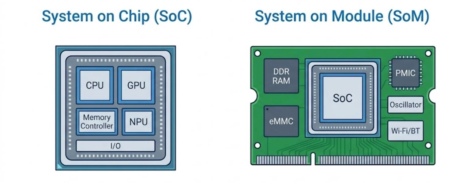
Figure: Showing an SoC as a single die and an SoM as a PCB carrying that SoC plus RAM, storage, and power chips.
SoC vs SoM: Side-by-Side Comparison
Selecting the right platform requires evaluating engineering resources, lifetime expectations, and product requirements. The table below compares these two approaches across key metrics.
| Design Metric | Chip-Down SoC Design | Modular SoM Design |
|---|---|---|
| Hardware Integration | Silicon chip level only | Pre-built module level |
| Onboard RAM & Storage | Must be designed on baseboard | Integrated on the module |
| PCB Layout Complexity | Extremely High (HDI, microvias, high layer count) | Low to Moderate (standard 2 to 4 layers for baseboard) |
| Development Cycle | Typically 12 to 24 months | Typically 3 to 6 months |
| Upfront NRE Cost | High (layout, validation, RF/EMC tooling) | Low (focused on carrier board validation only) |
| Per-Unit Bill of Materials (BOM) | Lower at high production scales | Higher (includes module margin) |
| Hardware Upgradeability | Difficult (requires complete PCB redesign) | Easy (drop-in pin-compatible modules) |
| Regulatory Certification | Full responsibility (FCC, CE, RoHS, RED) | Simplified (uses pre-certified RF/compute cores) |
| Product Lifecycle Management | Managed in-house (component obsolescence tracking) | Managed by the module vendor (7 to 15 years lifecycle guarantee) |
| Optimal Volume Range | Over 50k units per year | Under 50k units per year |
| Primary Industry Focus | Mass consumer, automotive, mobile | Industrial control, medical, IoT, edge AI |
Using a SoM significantly accelerates development. A typical chip-down SoC project can require 12 to 24 months of hardware engineering before the design is stable. Because every high-speed interface must be designed and verified from scratch, a single routing error can delay the schedule by months.
Conversely, a SoM arrives with verified memory routing, a validated power distribution network, a complete board support package (BSP), and a pre-ported operating system (such as Linux or Android). This allows software teams to begin application development immediately, reducing overall hardware development risks.
What Is a System on a Chip (SoC)?
A System on a Chip is a single integrated circuit that packs a complete computing core onto one piece of silicon. It holds processor cores and essential system logic on the same die, meaning it contains almost everything a device needs to compute, except for system memory, non-volatile storage, and physical power regulation.
What Components Are Integrated into an SoC?
Modern SoCs integrate massive functionality to reduce internal system latency and footprint:
- Multi-core Processors (CPUs): General-purpose processing units (e.g., ARM Cortex-A or RISC-V).
- Graphics Processors (GPUs): Specialized hardware acceleration for displays and rendering.
- Digital Signal Processors (DSPs): Accelerated math execution for audio, video, and sensor feeds.
- Neural Processing Units (NPUs): Hardware accelerators designed for on-device machine learning.
- Memory Controllers: Physical layer (PHY) and logical controllers for DDR3, DDR4, or LPDDR5 RAM.
- Integrated Interfaces: Built-in controllers for PCIe, USB, Ethernet, and SDIO.
- Wireless Transceivers: Select IoT-focused SoCs integrate physical Wi-Fi, Bluetooth, or Zigbee radios directly onto the die.
Challenges of Chip-Down SoC Design
Designing a board directly around a bare SoC is referred to as "chip-down" hardware design. This approach places the entire engineering and regulatory burden on your team. You must handle high-speed DDR routing with precise length matching and controlled impedance, implement multi-rail power management IC (PMIC) sequencing, resolve thermal dissipation bottlenecks, and manage electromagnetic compliance (EMC).
These tasks demand advanced layout tools and experienced hardware engineers. In particular, dealing with high-pin-count BGA package types requires high-density interconnect (HDI) PCBs, microvias, and blind/buried via stackups, which increase both engineering and manufacturing complexity.
Common SoC Examples
| SoC | Manufacturer | Architecture | Typical Use |
|---|---|---|---|
| Qualcomm Snapdragon | Qualcomm | ARM64 (Kryo) | Premium mobile and high-end IoT devices |
| NXP i.MX 8M Plus | NXP Semiconductors | ARM Cortex-A53 + M7 | Industrial HMI and machine vision systems |
| Rockchip RK3588 | Rockchip | ARM Cortex-A76 + A55 | Edge AI, NVRs, and high-performance media |
| TI AM62x | Texas Instruments | ARM Cortex-A53 + M4F | Industrial control and automotive displays |
- When you are ready to bring your design to life, JLCPCB provides fast, professional PCB assembly services.
- Whether you are building a custom SoM carrier board or a high-density, multi-layer chip-down SoC design, simply upload your Gerber files to receive an instant online quote and accelerate your product development.
What Is a System-on-Module (SoM)?
A System on Module is a small, specialized printed circuit board that houses an SoC and the supporting integrated circuits that the SoC cannot include on its own silicon. It packages the compute core, high-speed RAM, non-volatile storage, and critical clocking and power circuitry into a pre-engineered, unified module. It serves as a ready-to-use compute engine rather than a finished end-product.
What Components Are Included in a SoM?
- Host SoC: The primary processing unit of the module.
- System RAM: DDR3L, DDR4, or LPDDR4 memory chips routed with sub-millimeter precision.
- Non-Volatile Storage: eMMC, NAND flash, or SPI NOR flash containing the bootloader and operating system.
- Power Management IC (PMIC): Handles power conversion, buck/boost regulation, and precise voltage sequencing.
- System Clocks: Oscillators and crystals providing stable timing references.
- RF Modules (Optional): Shielded Wi-Fi and Bluetooth circuits, often pre-certified (FCC/CE).
- Board-to-Board Connectors: High-density, high-speed connectors (or castellated holes) to interface with external circuitry.
How a SoM Works with a Carrier Board
A SoM is designed to plug directly into a custom application-specific carrier board (or baseboard). This modular system splits hardware development into two distinct parts:
- The Compute Core (SoM): A standardized, complex subsystem that remains consistent across different projects.
- The Carrier Board: A custom PCB that contains only your specific application inputs/outputs (I/O), such as physical ports, sensor interfaces, and power inputs.
Understanding the structural differences between PCBA and PCB design helps clarify this approach. By using a pre-assembled SoM, the carrier board's routing is greatly simplified, typically requiring fewer board layers and avoiding high-density interconnect (HDI) manufacturing structures.
Popular System on Module Examples
| SoM | Host Processor | Primary Application Target |
|---|---|---|
| Toradex Verdin | NXP i.MX 8M Plus | Rugged industrial automation and medical devices |
| Variscite DART-MX8M | NXP i.MX 8M Family | Scalable embedded systems and IoT gateways |
| NVIDIA Jetson Orin Nano | NVIDIA Orin | Robotics, autonomous machines, and edge AI |
| Raspberry Pi CM4 / CM5 | Broadcom BCM2711 / BCM2712 | Cost-sensitive smart displays, kiosks, and prototyping |
| Digi ConnectCore 8M | NXP i.MX 8M Nano | Secure IoT networking and industrial control |
| AMD Kria K26 | Xilinx Zynq UltraScale+ | Real-time vision processing and factory automation |
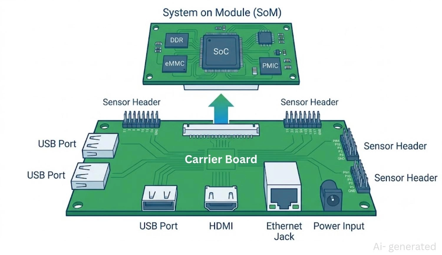
Figure: A SoM stacked on a larger carrier board, connected by a board-to-board connector, with application I/O on the carrier.
Real-World SoC and SoM Products
To better understand this design trade-off, let's examine how commercial products make this choice based on volume, size, and application limits:
- Smartphones (SoC): Modern smartphones operate on high-performance SoCs such as the Apple A18 or the Snapdragon 8 series. Extreme space constraints, high thermal dissipation requirements, and massive manufacturing runs (millions of units) make custom chip-down designs the only logical choice.
- Industrial HMI Panels (SoM): Factory control panels and human-machine interfaces (HMIs) typically ship in low-to-mid volumes (thousands of units per year). These designs often use modules like the Toradex Verdin or Variscite DART, trading a slightly higher bill of materials (BOM) cost for reliable long-term supply and accelerated development.
- Edge AI Smart Cameras (SoM): High-speed optical inspection systems often utilize an NVIDIA Jetson Orin Nano module. This allows the camera manufacturer to bypass the complex high-speed DDR and power delivery layout required by modern AI processors, focusing instead on optical sensors and software development.
- Wearable Fitness Bands (SoC): Smartwatches and fitness trackers require extremely compact footprints. They are typically designed around highly integrated, ultra-low-power SoCs, such as the Nordic nRF54 series. In this sector, meeting strict physical constraints through specialized wearable PCB assembly is essential, as standard SoMs are too large to fit.
This trend is consistent: consumer products focused on miniaturization and high volume lean toward SoC, while industrial, medical, and niche commercial systems prioritize SoM to reduce development risk and time-to-market.
Cost Comparison: System-on-Module vs System on a Chip
While unit cost is a major deciding factor, a complete analysis must weigh unit production costs against upfront non-recurring engineering (NRE) expenses.
A System on Module has a higher unit cost because you are paying the vendor for components, layout, and testing. A bare SoC is less expensive per unit but requires significant upfront development costs. These include:
- Senior hardware engineering layout time.
- Complex multi-layer PCB design runs (8 to 12 layers with microvias).
- Full RF, EMI, and safety certifications (e.g., FCC, CE).
- Production test fixture development.
At production volumes below 50,000 units per year, the SoM is usually the more economical choice. The savings in engineering hours, fast-tracked certifications, and simplified carrier boards outweigh the higher cost per module.
Above 50,000 to 100,000 units per year, the per-unit savings of a bare SoC justify the upfront design and certification costs, though recovering this investment can take one to two years of sustained production.
| Annual Production Volume | Upfront NRE Impact | Recommended Design Path |
|---|---|---|
| Under 10,000 units | NRE dominates total project cost | System on Module (SoM) |
| 10,000 to 50,000 units | SoM is typically more cost-effective | System on Module (SoM) |
| 50,000 to 100,000 units | Transition zone; evaluate internal design resources | Run a detailed cost/benefit analysis |
| Over 100,000 units | Upfront NRE is quickly amortized | Custom Chip-Down SoC |
To make an informed decision, design teams should carefully evaluate low-volume PCB assembly options early in the planning phase. The exact crossover point depends on several variables, including developer salaries, regulatory complexity, baseboard layer counts, and the product's expected market lifetime.
When to Choose a SoM
Choose a System on Module when time-to-market, risk mitigation, and development speed are your primary goals:
- Fast Time-to-Market: By utilizing a pre-validated module, you bypass time-consuming hardware debugging and bootloader development. This allows your team to focus directly on software application development from day one.
- Limited High-Speed Hardware Design Resources: If your engineering team does not have extensive experience with ultra-fine-pitch BGA routing, impedance matching, or high-speed memory tuning, using a SoM shifts this technical risk to the module vendor.
- Industrial and Medical Compliance: Many commercial SoMs are built specifically for demanding environments. They feature rugged designs, extended operating temperature ranges (typically -40 to +85 degrees Celsius), and comprehensive quality documentation.
- Long-Term Product Lifecycles: Reputable module manufacturers often guarantee component availability for 10 to 15 years. They also provide pin-compatible upgrade options, protecting your system from component obsolescence.
- Simplified Regulatory Certifications: Choosing a SoM with pre-certified wireless transceivers (such as FCC, CE, or IC) simplifies the regulatory process, reducing the risk of unexpected compliance delays.
When to Choose a Chip-Down SoC Design
Choose a chip-down SoC design when production volume, spatial optimization, and material costs are your main priorities:
- High Annual Production Volumes: When manufacturing over 50,000 to 100,000 units per year, saving even a few dollars per unit on material costs can quickly justify a substantial upfront engineering investment.
- Strict Size and Weight Constraints: Space-constrained designs like wearables, medical implants, and micro-drones cannot accommodate the physical height and footprint of a pluggable module.
- Aggressive Per-Unit Cost Targets: Eliminating the module vendor's markup and avoiding unused peripheral controllers on the SoM helps keep unit production costs as low as possible.
- Highly Custom Hardware Configurations: Designing your own board allows you to place only the components your application requires, optimize power distribution networks, and tailor the layout to your exact physical specifications.
- Established High-Speed Hardware Expertise: If your engineering team already has the layout tools and experience required for high-speed routing, high-density interconnect (HDI) design, and electromagnetic compatibility (EMC) troubleshooting, a chip-down design becomes a highly viable path.
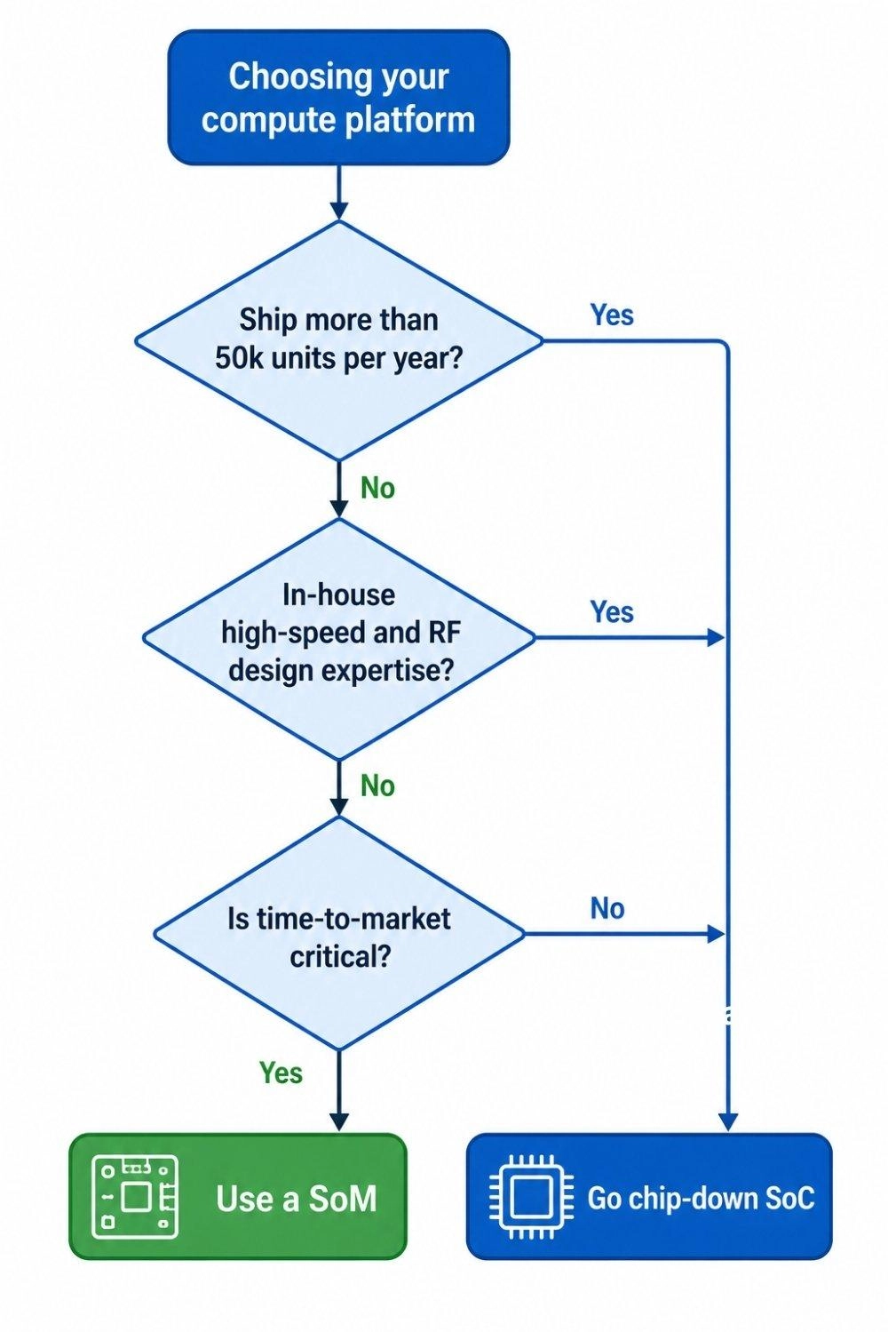
Figure: Flowchart routing volume, in-house expertise, and time-to-market questions toward either a SoM or a chip-down SoC.
The Hybrid Strategy: Start with a SoM, Then Migrate to an SoC
Selecting one architecture does not mean you are locked into it forever. Many successful product teams use a hybrid strategy: they launch their product using a SoM, then transition to a chip-down SoC design as sales volume increases.
This approach offers several key advantages:
- Fast-Tracked Product Launch: Using a SoM allows you to validate your product in the market, secure early customers, and refine your software application without a long development cycle.
- De-Risked Redevelopment: Once your product is proven and production volumes grow, you can redesign the system around the bare SoC. Because the software and carrier board interfaces have already been validated, migrating to a custom layout is much less risky.
- Managed Transition: Planning this migration carefully allows you to scale smoothly when scaling your PCBA prototype to low-volume production, ensuring a reliable supply chain at every stage of growth.
What Is a Carrier Board?
A carrier board (or baseboard) is the application-specific motherboard that a SoM plugs into. It houses the interfaces and physical connectors your product requires, such as USB, HDMI, Ethernet, and serial connections, along with power regulation and protective circuitry.
Because the complex, high-speed routing is contained within the pre-engineered SoM, carrier boards are much simpler to design. They can typically be routed on standard 2- to 4-layer PCBs, avoiding the expensive 8- to 12-layer HDI fabrication required for direct SoC designs. This greatly simplifies layout, prototyping, and testing.
To streamline manufacturing and ensure reliable component sourcing, you can search for and select compatible connectors, power components, and interfaces directly from the JLCPCB Parts Library.
How SoC, SoM, SBC, CoM, and SiP Differ
The embedded computing landscape uses several acronyms that frequently cause confusion. The primary differences lie in their level of integration and whether they require an external carrier board.
| Technology | Full Form | Hardware Description | Requires Carrier Board? |
|---|---|---|---|
| SoC | System on a Chip | A single integrated circuit containing processing cores and system controllers. | Yes, requires a custom PCB layout. |
| SiP | System in Package | Multiple separate silicon dies (e.g., CPU + RAM) are integrated inside a single package. | Yes, requires a custom PCB layout. |
| SoM | System on Module | A complete compute engine (SoC, RAM, storage, power) on a compact, pluggable PCB. | Yes, needs a carrier board for external I/O. |
| CoM | Computer on Module | An alternative term for a SoM; the two terms are often used interchangeably. | Yes, needs a carrier board for external I/O. |
| SBC | Single Board Computer | A complete, standalone computer with standard physical ports (e.g., Raspberry Pi) ready for use. | No, works out of the box. |
An SBC is a complete, off-the-shelf computer that works out of the box, making it well-suited for early prototyping or extremely low-volume projects.
A System in Package (SiP) packages multiple silicon dies into a single chip-like package, providing a middle ground between SoC and SoM, though it still requires a custom PCB layout.
Is a Compute Module the Same as a System on Module?
Yes. "Compute Module" is simply a vendor-specific term for a System on Module. The most well-known example is the Raspberry Pi Compute Module (CM4/CM5), which is a modular, industrial version of the standard Raspberry Pi single-board computer, designed specifically to be integrated into custom commercial products.
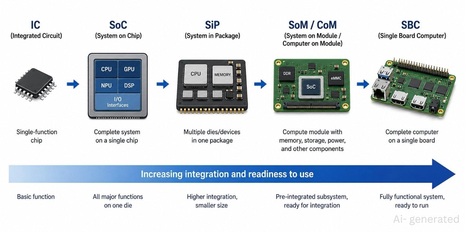
Figure: From IC to SoC to SiP to SoM/CoM to SBC showing rising integration and readiness to use.
FAQs about SoM and SoC
Q: How does choosing a SoM simplify FCC and CE compliance for industrial IoT products?
Using a pre-certified SoM with onboard wireless (Wi-Fi/Bluetooth) allows you to bypass expensive intentional radiator testing. Your end-product certification is often simplified to unintentional radiator testing, which reduces testing costs and shortens your compliance timeline.
Q: What are the main signal integrity challenges when designing a chip-down SoC carrier board?
The most demanding challenges involve high-speed signal integrity for DDR memory buses. This requires precise trace length matching to prevent skew, controlled impedance lines (typically 50 ohm single-ended and 100 ohm differential) to minimize reflections, and careful layer transitions to maintain a continuous ground reference plane.
Q: Why do high-performance SoCs require microvias and HDI PCB manufacturing stackups?
High-performance SoCs are typically packaged in fine-pitch Ball Grid Arrays (BGAs) with pitches of 0.8 mm, 0.5 mm, or smaller. Standard mechanical drilling cannot create vias small enough to exit the inner rows of pins. Designers must use laser-drilled microvias, blind vias, and buried vias to route these connections across inner routing layers.
Q: Can a customized carrier board be designed using a standard 4-layer PCB instead of an expensive high-density board?
Yes, this is one of the primary advantages of the modular approach. Because the complex high-speed connections and fine-pitch BGA breakouts are handled inside the multi-layer SoM, the carrier board only routes lower-speed peripherals and power lines. This allows the carrier board to be designed on a standard, low-cost 4-layer PCB.
Q: What is the risk of processor obsolescence when committing to a specific SoM vendor?
If a component on an SoC design goes end-of-life (EOL), you must redesign your entire board. With a SoM-based design, reputable vendors often guarantee 10+ years of product availability. Even if a specific module is phased out, vendors typically provide pin-compatible replacement modules, allowing you to upgrade your system without redesigning your carrier board.
Conclusion
For most low-to-mid-volume products, starting your design with a System on Module (SoM) is the most efficient path. It reduces development times, minimizes engineering risk, and simplifies regulatory compliance.
Custom chip-down SoC designs are best reserved for high-volume consumer products or space-constrained devices where physical size and per-unit material costs justify a substantial upfront engineering investment.
A practical, proven approach is to launch your product using a SoM to establish your market presence, then migrate to a chip-down SoC layout as production volumes scale.
Popular Articles
• SMD Resistor Package Sizes: Complete Size Chart, Footprints & How to Choose
• How to Solder SMD Components Like a Pro [2026 Updated]
• SMD Resistor Codes: How to Read 3-Digit, 4-Digit, and EIA-96 Markings
• SMD Capacitor Codes: Identification, Markings, and Polarity
• SMD Capacitor Sizes: Complete Size Chart and Selection Tips for PCB Design and Assembly
Keep Learning
SOIC Package: A Complete Guide to Specifications, Types, Uses, and SMT Assembly
As designs transition from legacy through-hole components to high-density Surface Mount Technology (SMT), the Small Outline Integrated Circuit (SOIC) remains the industry standard for operational amplifiers, flash memory, sensors, and microcontrollers. It reflects a well-balanced engineering design, offering a practical compromise between the miniaturisation demanded by modern consumer electronics and the ruggedness required for industrial applications. In this guide, you will learn: SOIC package dime......
What Is a 100nF Capacitor and How Do You Choose the Right One
Key Takeaways Value: A 100nF capacitor has a nominal capacitance of 0.1 µF, or 100,000 pF, and all three names describe the same part value. Marking: Many through-hole ceramic and film capacitors use the three-digit code 104, while most SMD MLCCs are unmarked. Main use: Its most common function is local decoupling at an IC power pin, where it supplies fast transient current and shunts high-frequency noise to ground. Default choice: For general decoupling, an X7R or X5R MLCC is a common starting point;......
SMD Resistor Package Sizes: Complete Size Chart, Footprints & How to Choose
Surface Mount Device (SMD) resistors are fundamental to modern electronics, and selecting the correct package size is a crucial engineering decision that impacts a PCB’s electrical performance, thermal reliability, and manufacturing cost. In this article, you will find practical, authoritative guidance on: The complete SMD resistor size chart (01005 to 2512) with exact dimensions and power ratings. Recommended PCB footprints and guidelines for reflow reliability. Critical trade-offs concerning power d......
PCB Connector Types Explained: Categories, Comparison, Applications and How to Choose the Right One
PCB connectors are essential components for connecting circuit boards with external devices, cables, or other PCBs. Choosing the right connector type affects signal reliability, mechanical stability, and overall product performance. Factors such as current rating, frequency requirements, pitch size, and mounting method should be considered during selection. In this guide, you will learn: The major types of PCB connectors and their applications. How different connector types compare. How to select the ......
What Is a System on a Chip (SoC)? A Complete Guide for PCB Designers
Nearly every electronic device you interact with today, from smartphones and IoT sensors to industrial controllers and AI edge systems, is powered by a System on a Chip (SoC). By integrating processors, memory controllers, communication interfaces, and specialized accelerators onto a single piece of silicon, SoCs deliver the performance, power efficiency, and compact form factors modern electronics demand. Whether you're selecting a processor for an embedded Linux design, evaluating an AI-capable plat......
Capacitors in PCB Design_ A Complete Guide to All Types
Capacitors are indispensable components in PCB (Printed Circuit Board) design, providing functionality from energy storage and noise filtering to voltage regulation. Whether you're designing a simple circuit or a complex multi-layer board, understanding the different types of capacitors and their applications is crucial. The basic structure of a capacitor consists of two metal plates separated by a layer of dielectric. Capacitors can be of fixed or variable type. The ability of the capacitor to hold e......