
Types of BGA Packages: Differences, Applications, and Selection Guide
11 min
- BGA Package Types Quick Comparison
- Types of BGA Packages Explained
- How to Choose the Right BGA Package for High-Speed and High-Reliability PCB Designs
- BGA Package Structure and Key Parameters Explained
- Conclusion
- FAQ about BGA
If you’re searching for the types of BGA packages, you’re likely trying to understand which one fits your PCB design, performance, or manufacturing needs. With options like PBGA, CBGA, and FBGA, each package comes with different trade-offs in thermal performance, cost, and reliability. Choosing the wrong type can lead to routing challenges, assembly defects, or even product failure.
In this guide, we break down all major BGA package types, compare their key differences, and explain how to select the right one for your application—so you can design with confidence and avoid costly mistakes.
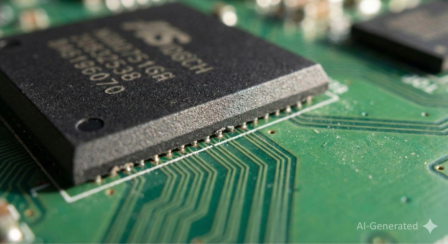
Figure: Macro view of a Ball Grid Array (BGA) package mounted on a high-density interconnect PCB.
BGA Package Types Quick Comparison
|
Package |
Ball Pitch Range |
Substrate Material |
Typical Applications |
Thermal Performance |
|---|---|---|---|---|
|
Plastic Ball Grid Array (PBGA) |
1.27mm - 1.0mm |
BT Resin, FR-4 |
Consumer electronics, MCUs |
Moderate |
|
Ceramic Ball Grid Array (CBGA) |
1.27mm |
Ceramic |
Aerospace, military |
Excellent |
|
Tape Ball Grid Array (TBGA) |
0.8mm - 0.5mm |
Polyimide tape |
Mobile devices |
Good |
|
Flip-Chip Ball Grid Array (FCBGA) |
1.27mm - 0.8mm |
Organic laminate |
High-performance processors |
Superior |
|
Micro BGA |
0.65mm - 0.4mm |
Thin organic |
IoT, wearables, sensors |
Moderate |
|
Thermally Enhanced BGA Packages |
1.27mm - 1.0mm |
Organic + Heat Spreader |
Power Amps, High-End FPGA |
Excellent |
|
Metal Ball Grid Array (MBGA) |
1.27mm - 1.0mm |
Metal (Aluminum) |
Industrial Motors, Amplifiers |
Excellent (θJA: <15℃/W) |
Types of BGA Packages Explained
#1 Plastic Ball Grid Array (PBGA)
Substrate Composition: PBGA makes use of a substrate made of BT (Bismaleimide Triazine) resin. The choice of BT resin instead of the standard FR-4 is because of its higher Glass Transition Temperature (Tg ≈ 180℃) and lower moisture absorption.
Thermomechanical Constraints: The primary failure mode in PBGAs is shear strain on the solder joints. This is caused by the Coefficient of Thermal Expansion (CTE) mismatch between the silicon die (2.6 ppm/℃) and the organic laminate substrate (≈ 13-17ppm/℃).
Moisture Sensitivity: PBGAs are known to absorb moisture. According to J-STD-020, the usual levels for them are MSL 3 and MSL 4. If the floor life limit is surpassed, they can't be used without baking at 125℃ - this is to prevent "popcorning," which is a very serious delamination issue caused by fast-expanding water vapor during reflow.
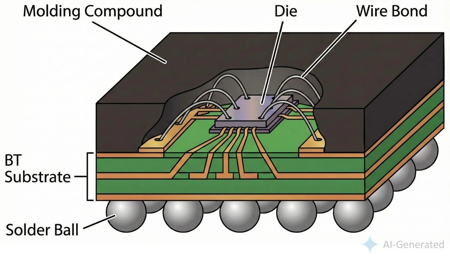
Figure: PBGA structure showing wire bonding and BT resin substrate layers.
Note
Do you need specific PBGA components for your PCBA? Check availability in the JLCPCB Parts Library.
#2 Ceramic Ball Grid Array (CBGA)
In cases where reliability is a must, even in extreme environments (Aerospace, Telecom), the Ceramic Ball Grid Arrays (CBGA) are the preferred option.
Substrate: Uses a multilayer co-fired ceramic (Al2O3) substrate.
CTE Matching: The ceramic substrate (CTE ≈ 6.7 ppm/℃) is nearly perfectly matched to the Silicon die. This leads to a large reduction of stress at the die-attach interface; however, the stress is then passed on to the PCB-to-package solder joints.
The "Non-Collapsing" Ball: Unlike PBGAs, CBGAs often utilize high-temperature solder balls (90Pb/10Sn) attached to the package with eutectic solder. During standard SMT reflow (SAC305 profile), the main sphere does not melt; only the eutectic interface reflows, maintaining a consistent standoff height.
#3 Flip-Chip Ball Grid Array (FCBGA)
For high-performance computing (CPUs, GPUs, ASICs), wire bonds introduce unacceptable inductance. Flip-Chip BGA (FCBGA) replaces wires with C4 (Controlled Collapse Chip Connection) bumps.
Inductance Reduction: A typical wire bond introduces 2 - 3nH of parasitic inductance. C4 bumps reduce this to <0.2nH, which is essential for high-speed SerDes lanes (>10 Gbps).
Power Delivery Network (PDN): The vertical pathway provides lower impedance (ZPDN), which significantly helps reduce voltage droop (Vdroop) during high di/dt switching.
Underfill Physics: Because the die is rigidly attached to the substrate via bumps, a capillary underfill epoxy is injected between the die and substrate. This material is engineered to redistribute thermomechanical stress and prevent bump cracking (fatigue failure).
|
Parameter |
FCBGA |
Wire-bonded PBGA |
Performance Gain |
|---|---|---|---|
|
Parasitic Inductance |
0.2-0.5 nH |
2-5 nH |
5-10× reduction |
|
Max Frequency |
>5 GHz |
2-3 GHz |
>60% improvement |
|
Thermal Resistance (θJC) |
0.1-0.3°C/W |
1-3°C/W |
5-10× improvement |
|
Power Delivery |
<5 mΩ |
15-30 mΩ |
3-6× improvement |
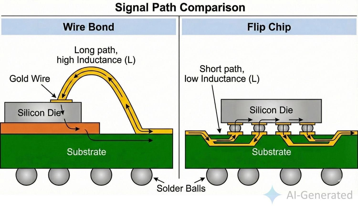
Figure: Signal path inductance comparison between wire-bond BGA and flip-chip BGA technology.
#4 Tape Ball Grid Array (TBGA)
The technology used in Tape Ball Grid Arrays consists of a flexible polyimide tape substrate with 25 - 75𝜇m thickness and copper circuit layers.
Thermal Performance: TBGAs are normally constructed in a "cavity-down" configuration, which gives the die backside direct attachment to a heat spreader.
Application: Ideal for thin-profile mobile devices requiring moderate pin counts and excellent thermal dissipation.
#5 Micro BGA
Micro BGAs (μBGA) are a common form of Chip Scale Package (CSP), typically with a footprint no more than 1.2× the die size. They are widely used in smartphones, wearables, and memory devices where space is critical.
Extreme Fine Pitch: Ball pitch is typically reduced to 0.5 mm down to 0.3 mm or below, requiring tight placement accuracy and precise stencil design.
Solder Paste Considerations: At pitches below 0.4 mm, Type 4 solder paste may face printability limitations depending on stencil and process control, making Type 5 or finer paste more suitable for consistent deposition.
Reliability and Reinforcement: Due to small solder joint volume and CTE mismatch, μBGAs are more susceptible to mechanical and thermal fatigue. Underfill (capillary or corner bonding) is commonly used to improve drop and thermal reliability.
Manufacturing Impact: Fine pitch and hidden solder joints make inspection and rework more challenging, requiring X-ray inspection and tight process control.
#6 Thermally Enhanced BGA Packages (e.g., ePBGA)
Thermally enhanced BGA packages are designed for power-intensive applications (typically 5–20 W and beyond) where heat dissipation is critical.
Construction: These packages integrate a metal heat spreader or “slug” (commonly copper or aluminum) into the package structure. The die is attached directly to this thermal interface, providing a low thermal resistance path for efficient heat transfer.
Thermal Performance: Compared to standard PBGA, thermally enhanced BGAs can significantly improve junction-to-case thermal resistance (θJC) and overall heat dissipation, depending on PCB implementation.
PCB Design Note: To fully utilize the thermal advantages, designers should use dense thermal vias (often via-in-pad, filled or capped) beneath the package to transfer heat into internal planes. Proper copper distribution and stack-up design are critical for optimal performance.
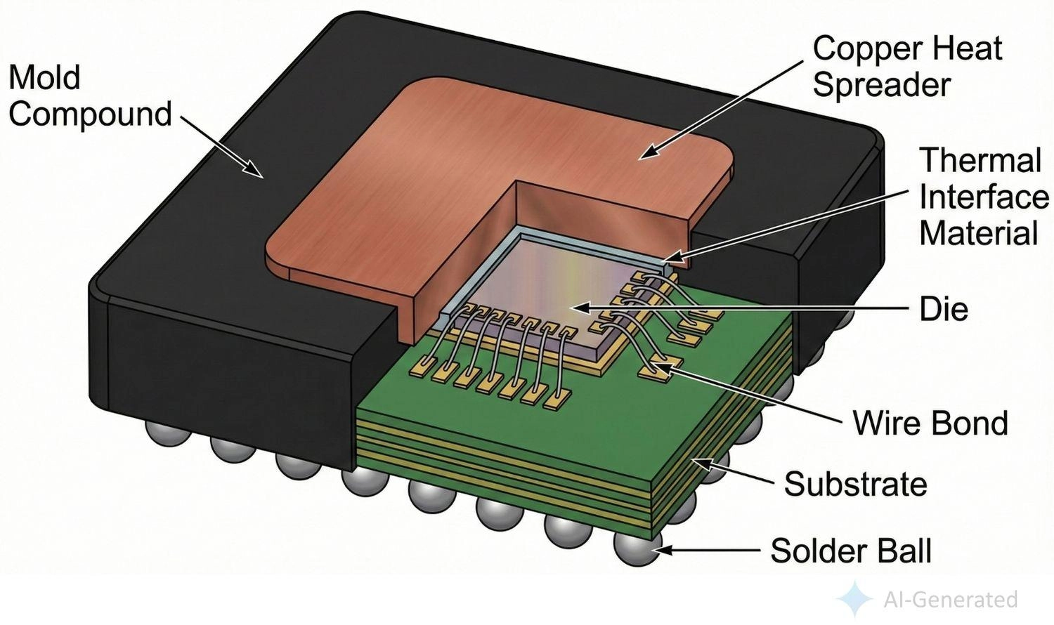
Figure: Enhanced BGA structure with integrated heat sink for thermal management.
#7 Metal Ball Grid Array (MBGA)
The Metal Ball Grid Array (MBGA) utilizes a metal substrate (typically anodized Aluminum) rather than the standard organic or ceramic substrates found in other types.
Construction: The silicon die is attached to the metal substrate using a thermally conductive adhesive. A thin-film circuit layer is laminated to the metal to provide electrical routing, connected via wire bonding.
Thermal Physics: The aluminum core acts as a massive integrated heat sink. This allows MBGA to achieve thermal performance comparable to Ceramic BGA (CBGA) but at a significantly lower cost point.
Applications: MBGA is the preferred choice for industrial motor controllers, high-power operational amplifiers, and telecom line cards where heat dissipation is the primary design constraint.
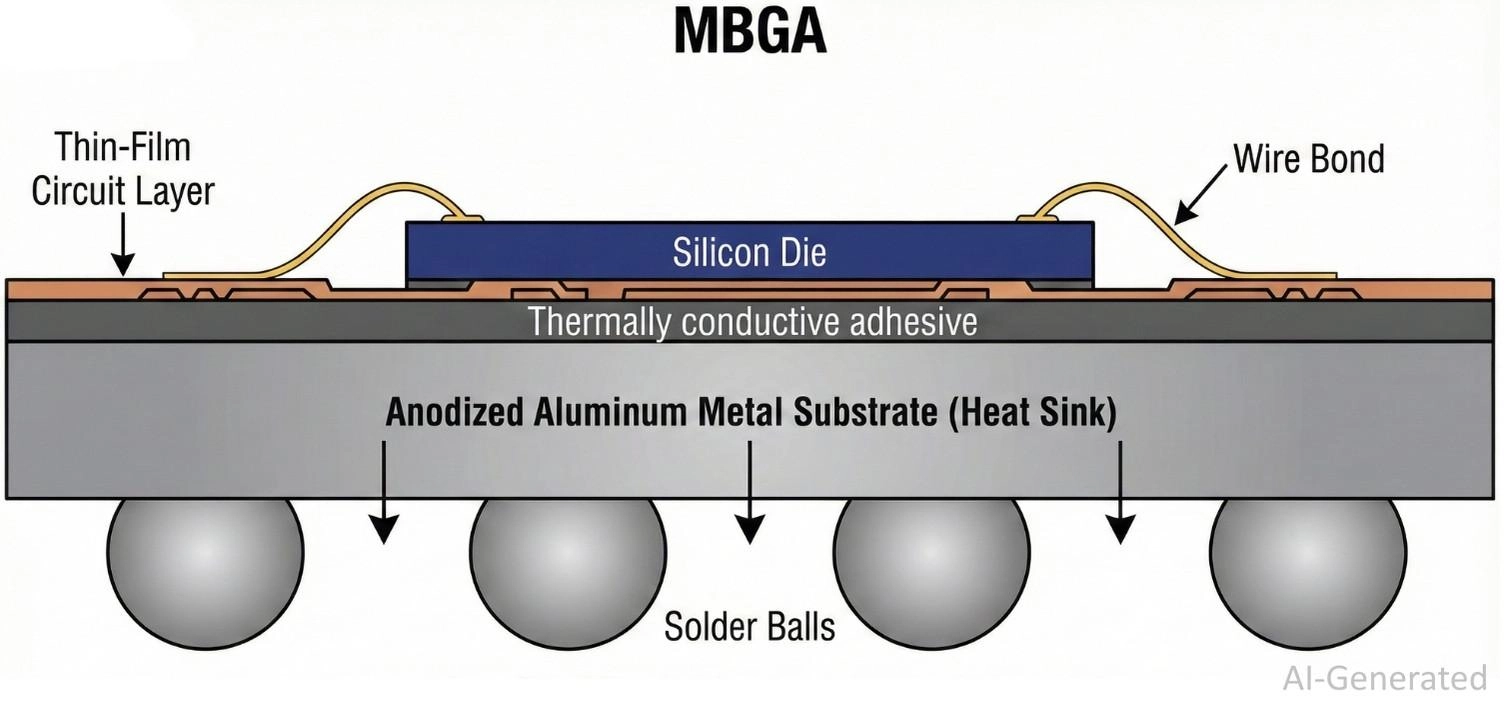
Figure: Metal Ball Grid Array package structure showing an aluminum substrate for heat dissipation.
How to Choose the Right BGA Package for High-Speed and High-Reliability PCB Designs
The selection of a suitable BGA package implies the systematic scrutiny of the Electrical, Thermal, Mechanical, and Cost parameters.
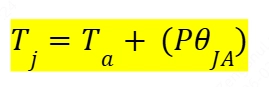
If passive cooling cannot maintain Tj < 100℃, upgrade to CBGA or EBGA variants.
|
Application Domain |
Recommended BGA |
Key Selection Factors |
Cost Tier |
|---|---|---|---|
|
Consumer Electronics |
PBGA |
Cost-effectiveness, adequate performance |
$ |
|
Mobile/Wearables |
TBGA, Micro BGA |
Ultra-thin profile, fine pitch I/O |
$$ |
|
High-Performance Computing |
FCBGA |
Maximum electrical performance, low ZPDN |
$$$ |
|
Aerospace/Military |
CBGA, CGA |
High reliability, CTE matching, ruggedness |
$$$$ |
|
IoT Sensors |
Micro BGA |
Miniaturization, low profile |
$$ |
|
Power Electronics |
EBGA |
Enhanced thermal management (>10W) |
$$$ |
BGA Package Structure and Key Parameters Explained
The core BGA comprises five major components: the substrate (organic or ceramic), die-attachment area, interconnect structure (wire bonds or flip-chip bumps), encapsulation material, and solder-ball array.
Among them, the substrate serves as both a mechanical carrier and an electrical interface, conducting signals from the die to the peripheral connections.
The following critical parameters define the performance characteristics of BGA:
- Ball Pitch: The distance between the centers of the two solder balls is 1.5mm for the oldest designs, and it goes down to 0.4mm for the extremely fine-pitch types.
- Substrate Materials: BT (bismaleimide triazine) resin is the best choice because of the electrical characteristics, FR-4 is the best option because of the price, while the ceramic substrate has the best thermal conductivity and the same CTE as silicon.
- Solder Composition: Traditional eutectic SnPb (63/37 tin-lead) has largely been replaced by lead-free alternatives like SAC305 (96.5% tin, 3% silver, 0.5% copper) and SAC405. These alloys are different in melting temperature and mechanical properties, which are the main factors for JLCPCB PCB assembly reflow processes.
Conclusion
Not all types of BGA packages are interchangeable—your choice directly affects routing complexity, thermal performance, and assembly yield.
- Use PBGA for cost-sensitive, general-purpose designs.
- Choose CBGA when thermal stability and reliability are critical.
- Go with FBGA or fine-pitch BGA for high-density, high-speed applications where space and signal integrity matter.
Before finalizing your selection, always verify ball pitch compatibility, PCB stack-up capability (HDI or not), and assembly limits such as reflow control and inspection access.
In practice, the “best” BGA package is the one your PCB design and manufacturing process can reliably support—not just the one with the highest performance on paper.
Reliable implementation requires a manufacturing partner who understands the physics of reflow. With capabilities for 0.35mm pitch assembly, 10-zone reflow profiling, and 100% 3D X-Ray inspection, JLCPCB ensures that your high-density designs perform as simulated.
Ready to prototype? Get an instant quote for your High-precision BGA assembly at JLCPCB.
FAQ about BGA
Q: What is the most common BGA type?
The PBGA (Plastic Ball Grid Array) is the industry standard for most consumer and industrial electronics. It is highly cost-effective, offers excellent electrical performance, and provides a reliable solder joint due to the coefficient of thermal expansion (CTE) matching well with standard FR-4 PCB materials.
Common Applications: Microprocessors, memory chips (DDR), and networking controllers.
Q: Which BGA has the best thermal performance?
For high-wattage applications, Thermally Enhanced BGA (ePBGA) and FCBGA (Flip Chip BGA) are the top performers. They can handle 5W to 20W+ depending on the airflow and PCB thermal via design.
Q: What is the difference between PBGA and CBGA?
The primary difference lies in the substrate material:
PBGA (Plastic): Uses a plastic-based laminate. It's lighter and cheaper but has lower thermal conductivity.
CBGA (Ceramic): Uses a ceramic substrate. It offers superior reliability in extreme temperatures and high-frequency environments (like aerospace or telecommunications) but is more expensive and requires careful CTE management to avoid solder joint cracking.
Popular Articles
• SMD Diode Code Lookup: Full List, Marking Guide & Identification [2026 Guide]
• SMD Resistor Package Sizes: Complete Size Chart, Footprints & How to Choose
• SMD Capacitor Codes: Identification, Markings, and Polarity
• SMD Capacitor Sizes: Complete Size Chart and Selection Tips for PCB Design and Assembly
• How to Solder SMD Components Like a Pro [2026 Updated]
Keep Learning
PoP Package (Package on Package) Explained: Architecture, Assembly, and SMT Challenges
In the race for miniaturization, fitting more processing power into smaller footprints is the ultimate challenge for PCB designers. Package on Package (PoP) technology answers this by integrating logic and memory vertically, becoming the standard for modern mobile processors. However, this 3D architecture demands advanced SMT assembly capabilities beyond standard fabrication. JLCPCB specializes in the high-precision manufacturing required to master these complex stacks. This guide covers how PoP packa......
What Is a PQFP Package? Plastic Quad Flat Package Design, Footprint, and Assembly Guide
The Plastic Quad Flat Package (PQFP) is a widely used IC package in industrial, automotive, and embedded designs. This article provides a practical, engineering-focused guide to PQFP package. It explains how PQFP is built, when it makes sense to use it, how it compares with newer package types, and what designers should consider in terms of footprint design, thermal performance, signal integrity, manufacturing, and reliability. What Is a PQFP Package (Plastic Quad Flat Package)? A Plastic Quad Flat Pa......
Small Outline Integrated Circuit (SOIC): Package, Specs & Uses
As designs transition from legacy through-hole components to high-density Surface Mount Technology (SMT), the Small Outline Integrated Circuit (SOIC) remains the industry standard for operational amplifiers, flash memory, sensors, and microcontrollers. It stands as a testament to balanced engineering, offering a perfect compromise between the miniaturisation demanded by modern consumer electronics and the ruggedness required for industrial applications. This article serves as a definitive engineering ......
A Complete Guide to Surface Mount Device (SMD)
Imagine holding a smartphone in your hand. Inside that sleek device lies a complex network of thousands of miniature components — resistors smaller than a grain of rice, capacitors thinner than a fingernail, and integrated circuits containing millions of transistors. Without Surface Mount Technology (SMT) and its compact Surface Mount Devices (SMDs), none of this would exist. Just a few decades ago, electronics were bulky. Radios filled desks, computers filled rooms, and assembling a circuit meant dri......
Circuit Breaker Types Explained: MCB, MCCB, RCCB, RCBO, ACB, VCB & SF6 Circuit Breakers
A circuit breaker automatically disconnects power when it detects faults such as overloads or short circuits, protecting equipment and reducing fire risk. Different circuit breaker types are designed for different voltage levels, current ratings, and applications, from household distribution boards to high-voltage substations. This guide explains the most common types - including MCBs, MCCBs, RCCBs, RCBOs, ACBs, VCBs, and SF6 breakers and helps you choose the right one for your application. Figure: Ci......
Quad Flat Package (QFP): The Engineer's Guide to Design, Assembly and Thermal Management
What is QFP Package? The Quad Flat Package (QFP) is one of the most popular surface mount technology (SMT) package formats throughout the history of electronic manufacturing. After it became standard in the 1980s, the QFP has been the industry standard for integrated circuits (ICs) with moderate to high pin counts that typically range from 32 to 304 pins, so it was a good alternative for simple SOIC packages and complex Ball Grid Arrays (BGAs) at the same time. Defined by its "gull-wing" leads extendi......