
What Is a System on a Chip (SoC)? A Complete Guide for PCB Designers
18 min
- What Is a System on a Chip?
- Common Examples of System on Chip
- How System on a Chip Works
- Main SoC Components
- Understanding SoC Architecture
- SoC vs. Microcontroller (MCU)
- SoC vs. Microprocessor (MPU)
- SoC vs. FPGA
- System on a Chip: Pros and Cons
- Common Applications of System on a Chip
- The Rise of AI System-on-Chip
- How to Select the Right System on a Chip for Your Design
- System on a Chip vs. System on Module vs. System in Package
- FAQs About System on a Chip
- Conclusion
Nearly every electronic device you interact with today, from smartphones and IoT sensors to industrial controllers and AI edge systems, is powered by a System on a Chip (SoC). By integrating processors, memory controllers, communication interfaces, and specialized accelerators onto a single piece of silicon, SoCs deliver the performance, power efficiency, and compact form factors modern electronics demand.
Whether you're selecting a processor for an embedded Linux design, evaluating an AI-capable platform, or comparing SoCs against MCUs and FPGAs, understanding SoC architecture is essential for professional hardware development.
In this deep-dive guide, you will learn:
- What a System on a Chip is
- How SoCs move data internally
- The main components found inside modern SoCs
- Differences between SoCs, MCUs, MPUs, and FPGAs
- How AI accelerators fit into modern SoC designs
- How to choose the right SoC for a project
What Is a System on a Chip?
A System on a Chip (SoC) is an integrated circuit that combines all the essential components of a complete electronic system onto a single semiconductor die. Where a traditional computer system distributes processing, memory, graphics, and I/O across multiple chips connected by a PCB, an SoC integrates all of these functions into one package, sharing silicon area, power rails, and high-bandwidth on-chip interconnects.
The critical distinction is integration level. An SoC is not simply a fast processor; it is a complete system that integrates compute, memory control, communication, and control logic on a single die.
Why SoCs Matter in Modern Electronics
The shift from discrete multi-chip designs to SoCs was driven by two core compounding pressures:
- Miniaturization: Mobile devices, wearables, and IoT nodes demand PCB areas that make discrete chip layouts impossible. One BGA package replaces a CPU, GPU, memory controller, wireless IC, and power management chip.
- Power efficiency: On-die interconnects are orders of magnitude shorter than PCB traces. Shorter wires mean lower capacitance, lower switching energy, and tighter power-domain control with per-block clock gating and DVFS (Dynamic Voltage and Frequency Scaling).
Common Examples of System on Chip
SoCs span an enormous performance and integration range:
- Qualcomm Snapdragon 8 Elite, a flagship mobile SoC, integrates custom Oryon CPU cores, an Adreno GPU, a next-generation NPU, a 5G modem, ISP, and Wi-Fi 7 on a cutting-edge TSMC 3 nm process node.
- Apple M-series (M5), a PC-class SoC fabricated on an advanced 3 nm process node, utilizes a massive transistor budget and an ultra-fast unified memory architecture.
- Espressif ESP32-S3, a wireless IoT SoC built on a TSMC 40 nm process, features a dual-core Xtensa LX7 and Wi-Fi + BLE on-chip.
- STM32MP1, an industrial SoC with dual Cortex-A7 and Cortex-M4 cores, targets real-time and Linux co-processing.
To accommodate these highly integrated packages on a physical circuit board, hardware engineers must design complex breakout traces. This is typically achieved using high-density interconnect (HDI) routing techniques and specialized BGA package types to ensure structural and electrical integrity.
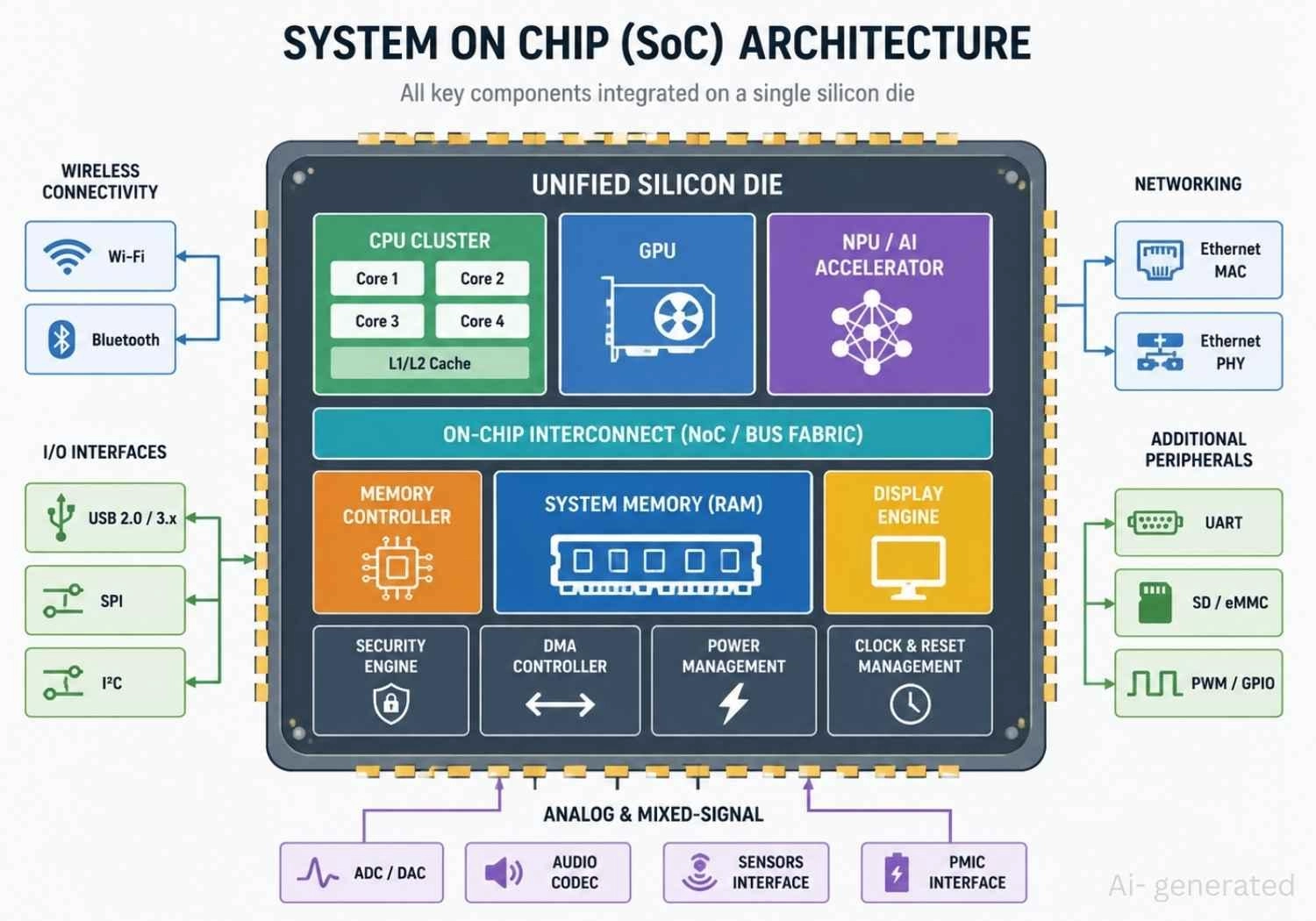
Figure: System on a Chip architecture highlighting major functional blocks: processing units (CPU, GPU, NPU), unified memory controller, and peripheral buses including USB, SPI, I2C, Ethernet, and Wi-Fi.
How System on a Chip Works
Integrating an Entire System on One Die
In a discrete multi-chip design, a processor communicates with a GPU over PCIe lanes, accesses DRAM through a separate memory controller IC, and reaches peripherals via a chipset, with all signals traveling across PCB traces at limited bandwidth and with measurable propagation delay and power loss at every interface.
An SoC eliminates all of those external paths. Every functional block, including CPU cores, GPU, memory controller, wireless radio, and peripheral controllers, shares the same silicon substrate and communicates through on-die interconnects. The result is drastically higher bandwidth, lower latency, and lower power per operation.
Internal Data Flow and On-Chip Interconnects
The on-chip interconnect fabric is the performance-critical structural layer of the SoC. It orchestrates all internal data paths:
- CPU core fetches instructions from L1 instruction cache.
- L1/L2/L3 cache hierarchy absorbs the majority of memory requests, avoiding costly DRAM accesses.
- Memory controller arbitrates DRAM requests that miss the cache, driving external LPDDR or DDR memory via an on-die PHY interface.
- DMA (Direct Memory Access) controllers move bulk data (such as camera frames, audio buffers, and network packets) between peripherals and memory without burdening the CPU.
- Peripheral subsystem (USB, PCIe, MIPI, UART, SPI, I2C) communicates with the outside world through the outer I/O ring.
Rather than relying on outdated shared parallel buses that choke under concurrent data requests, modern SoCs utilize packet-switched routing and dedicated point-to-point interconnect channels to maintain gigabytes-per-second throughput across individual IP blocks.
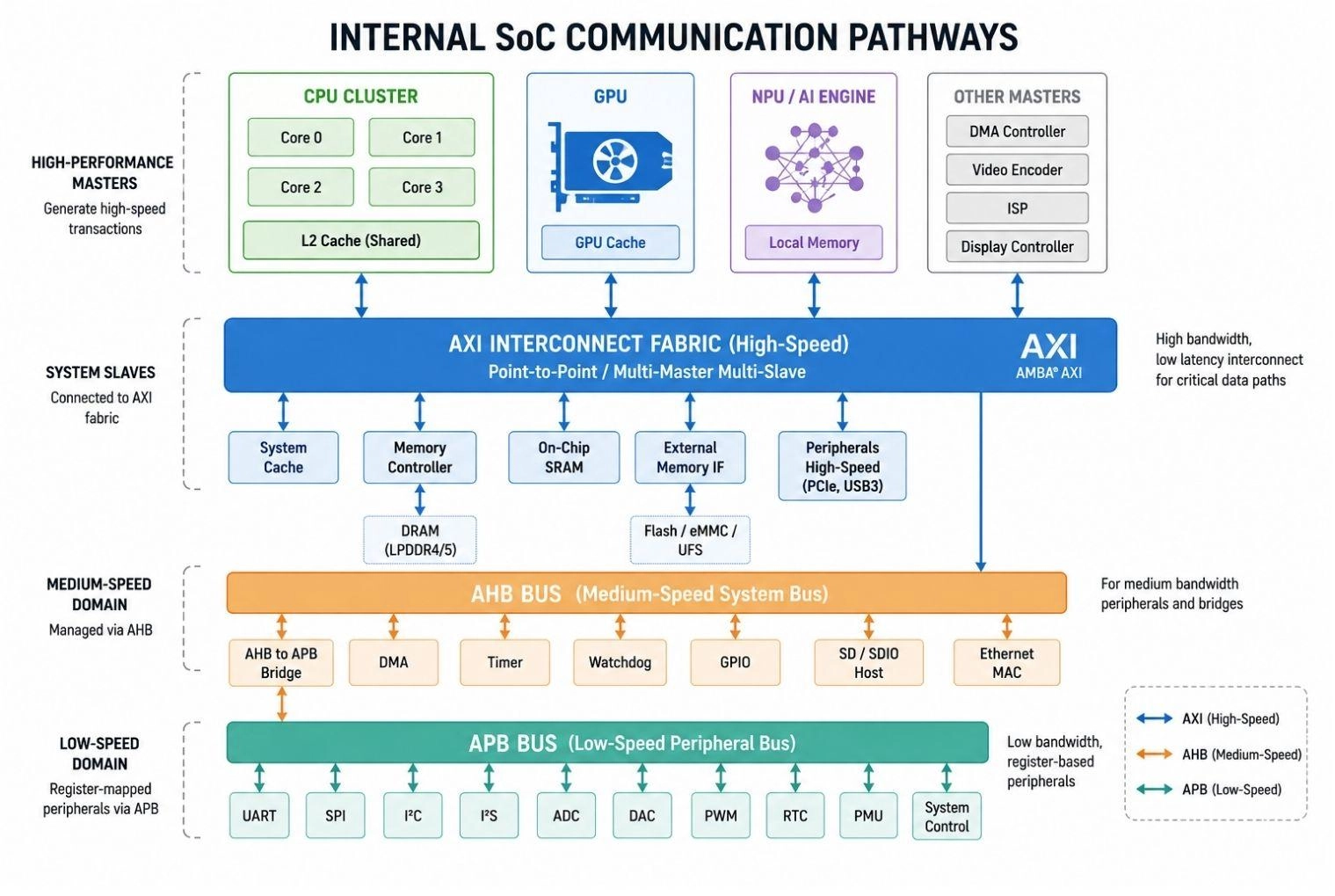
Figure: Internal data flow of an SoC, visualizing how high-speed processing cores communicate via AXI interconnects, bridging to AHB and APB bus protocols.
Main SoC Components
Most application-class System on a Chips rely on a common set of foundational hardware blocks built into the physical silicon:
- CPU Cores: The processor subsystem is the programmable heart of the SoC. Most application-class SoCs use Arm Cortex-A cores for general-purpose workloads, Cortex-M cores for low-power management, and Cortex-R cores for real-time responsiveness. RISC-V processors are increasingly common in wireless and microcontroller-class SoCs, such as the dual RISC-V Hazard3 cores on the Raspberry Pi RP2350.
- GPU: Handles graphics rendering and parallel compute workloads (GPGPU). Modern chips leverage architectures like the Adreno series or Mali-400 MP2 to process display assets and accelerate machine learning mathematical operations.
- NPU and AI Accelerators: A highly specialized coprocessor optimized specifically for the matrix multiply-accumulate operations that dominate neural network inference. By using dedicated matrix math arrays, NPUs (like the advanced Apple M5 Neural Engine) execute complex model math at a fraction of the power required by general-purpose CPUs.
- Memory Subsystem: An integrated hierarchy combining on-die SRAM (L1, L2, and shared L3 caches) with an on-die DDR controller/PHY interface designed to arbitrate high-speed memory transactions with external DRAM.
- Communication Interfaces: Physical controllers routing data to external interfaces. These are split between high-speed buses (PCIe, USB 3.x, MIPI CSI/DSI, GbE) and low-speed peripheral interfaces (UART, SPI, I2C, GPIO).
- Power Management Unit (PMU): Manages internal clock gating, maps out power domains, and communicates with external PMICs to control dynamic frequency scaling (DVFS).
- Security Engines: Hardware blocks enforcing cryptographic isolation. These include secure boot ROMs, Arm TrustZone boundaries, hardware-accelerated crypto engines (AES, SHA, ECC), and OTP eFuses to store immutable device cryptographic keys.
Understanding SoC Architecture
Heterogeneous Processing
Modern SoCs typically implement heterogeneous processing: multiple processor types operating concurrently on a single die, with each core optimized for a specific workload class. A typical application SoC integrates a CPU cluster (for serial logic and operating system coordination), a GPU (for parallel graphics and display rendering), an NPU (for neural network acceleration), and real-time controller cores (such as Cortex-M or RISC-V coprocessors) for power management and low-latency hardware interaction.
By offloading specialized math and control tasks to dedicated, hardware-accelerated blocks rather than processing everything through the main CPU, the system achieves maximum computational efficiency and significantly reduces overall power draw.
Memory and Interconnect Architecture
Because transferring data between subsystems draws significant power and introduces latency, memory and bus architectures are key to SoC performance:
- Cache Hierarchies: Working data is staged across multiple cache levels on-die. This includes single-cycle private L1 caches, cluster-level L2 caches, and a large shared L3 or Last Level Cache (LLC) that prevents costly, high-latency data fetches from external DRAM.
- On-Chip Interconnects (AMBA standard): Functional blocks communicate using the industry-standard Arm AMBA (Advanced Microcontroller Bus Architecture) protocol. Rather than four separate sub-buses, the system routes data dynamically: APB manages low-speed peripherals, AHB orchestrates medium-bandwidth transfers, AXI handles high-performance memory traffic, and Network-on-Chip (NoC) scales communications for massive multicore layouts.
- Power Islands and Clock Gating: Modern architectures dynamically divide the die into isolated power domains. System hardware dynamically switches off voltage rails (power islands) or halts clocks (clock gating) to idle blocks cycle-by-cycle, minimizing both active and static leakage currents.
SoC vs. Microcontroller (MCU)
A microcontroller integrates a CPU, small SRAM, flash, and basic peripherals (UART, SPI, I2C, ADC, timers) on one die, optimized for cost-sensitive, control-dominated tasks running bare-metal firmware or a lightweight RTOS.
An SoC extends this integration dramatically by adding a GPU, NPU, DSP, GHz-class multicore CPUs, gigabytes of DRAM via an integrated controller, and high-speed interfaces (PCIe, USB 3, MIPI). Application SoCs run full Linux or Android.
SoC vs. Microprocessor (MPU)
A microprocessor (MPU) is a CPU-only chip that requires external memory controllers, GPU, and peripheral ICs to form a complete system. Modern x86 processors have absorbed the memory controller and integrated GPU onto the same die, making them increasingly SoC-like, but they still require external chipsets and platform hubs, preserving the distinction.
SoC vs. FPGA
An FPGA (Field-Programmable Gate Array) contains a fabric of configurable logic cells that can be programmed to implement any digital circuit after manufacturing. FPGAs offer maximum flexibility and deterministic timing, but they consume more power per operation and require hardware description layouts to program.
FPGA SoC (such as the AMD Zynq UltraScale+ MPSoC) combines a hard ARM processing system with a programmable logic (PL) fabric on the same die. This supports running an operating system like Linux on the processor cores while implementing custom real-time logic in the FPGA fabric.
| Attribute | MCU | MPU | SoC | FPGA | FPGA SoC |
|---|---|---|---|---|---|
| Fixed Logic | Yes | Yes | Yes | No | Partial |
| Post-Silicon Programmability | Firmware only | Firmware only | Firmware only | Full hardware | Firmware + logic |
| Typical OS | Bare-metal / RTOS | Linux (ext. chips) | Linux / Android | None / bare-metal | Linux + custom RTL |
| Peripheral Integration | High | Low | Very high | None (add in fabric) | High + custom |
| Unit Cost (Volume) | $1–$15 | $5–$50 | $5–$200+ | $5–$500+ | $20–$500+ |
| Best-fit Use Case | Control, low-cost IoT | Legacy layouts | Linux, AI edge | DSP, custom logic | Mixed RTOS + RTL |
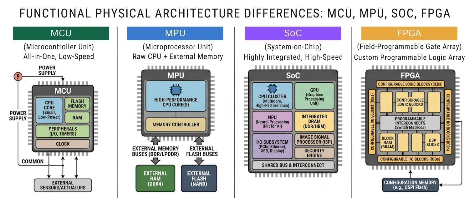
Figure: Physical architecture differences: MCU (all-in-one low-speed), MPU (CPU only), SoC (highly integrated high-speed), and FPGA (custom programmable logic array).
System on a Chip: Pros and Cons
Understanding the structural advantages and limitations of SoCs helps hardware engineers balance performance targets against production complexities:
Advantages of SoC
- Smaller PCB footprint: Integrating processing, memory, and peripheral domains onto a single package reduces overall board area, enabling compact mobile, IoT, and wearable designs.
- Lower power consumption: Shorter on-die interconnects exhibit less capacitance and switching loss than board-level traces.
- Superior memory bandwidth: Co-packaged DRAM allows gigabytes-per-second memory transfer rates that traditional board-level routing cannot support at low power.
- Reduced BOM and manufacturing costs: Consolidating multiple physical ICs down to one SoC lowers material counts, reduces the required PCB layer count, and limits assembly points of failure.
Disadvantages of SoC
- High thermal density: Concentrating multiple high-frequency subsystems (CPU, GPU, NPU) on one tiny silicon package generates significant heat, necessitating careful thermal design and PCB layout planning.
- No hardware upgradeability: Subsystems are locked in silicon. A failure in one peripheral block, or an outdated communication module, requires replacing the entire chip.
- High design and bring-up complexity: Designing for application-class SoCs requires extensive experience in high-speed routing, complex power sequencing, and board support package (BSP) compilation.
Common Applications of System on a Chip
SoC devices act as the primary computing engine across a wide array of modern hardware platforms:
- Smartphones and Tablets: Mobile platforms rely on highly integrated SoCs (such as the Snapdragon 8 Elite) to run multi-GHz custom processing clusters, high-frequency modems, and graphical engines within a minimal physical footprint.
- IoT Devices: Low-power wireless SoCs integrate RF front-ends, hardware cryptographical zones, and optimized sleep states to extend deployment lifespans on tiny battery cells.
- Industrial Automation: Industrial edge controllers prioritize reliable, deterministic physical communication buses like CAN-FD and gigabit Ethernet with Time-Sensitive Networking (TSN).
- Automotive Electronics: Infotainment systems, body control hubs, and ADAS hardware utilize functional safety-certified SoCs to satisfy stringent ASIL standards.
- AI Edge Computing: Smart cameras and robotic systems leverage dedicated NPUs to run complex neural network inference locally without offloading private data to cloud services.
- Networking Equipment: Enterprise switches and security appliances depend on packet-routing SoCs with integrated gigabit MAC engines and hardware-accelerated deep packet inspection.
The Rise of AI System-on-Chip
Why AI Workloads Need Specialized Hardware
Neural network inference is dominated by one operation: multiply-accumulate (MAC) across large matrices. Processing blocks handle these operations with vastly different performance and efficiency profiles:
- CPU (Central Processing Unit): Low parallelism, maximum operational flexibility, and low power efficiency for matrix math. It is best suited for serial control logic and general OS task coordination.
- GPU (Graphics Processing Unit): High parallelism, high programming flexibility, and moderate power efficiency. It is best suited for parallel graphics workloads and model training.
- NPU (Neural Processing Unit): Ultra-high fixed parallelism, minimal programming flexibility, and superior power efficiency. It is optimized to execute high-throughput, low-power model inference at the edge.
Edge AI Processing in SoC
Edge AI means running inference on-device rather than in the cloud. The practical benefits are concrete: sub-millisecond latency (no network round-trip), no data leaving the device (privacy compliance), operation without network connectivity, and elimination of per-query cloud API cost. These factors are driving NPU integration into almost every new application-class SoC.
Examples of AI SoC
- Apple M5: Features a next-generation Neural Engine delivering industry-leading TOPS (Trillions of Operations Per Second) to accelerate on-device Apple Intelligence and localized machine learning models effortlessly.
- Qualcomm Snapdragon 8 Elite: Integrates a highly advanced NPU engineered for real-time multimodal generative AI, live translation, and advanced on-device LLMs.
- NXP i.MX 8M Plus: 2.3 TOPS NPU targeting industrial vision and voice-UI at the edge (Electronic Design / NXP).
- Intel Meteor Lake / Lunar Lake: integrated NPU for Windows AI PC workloads (Microsoft Copilot+ tier).
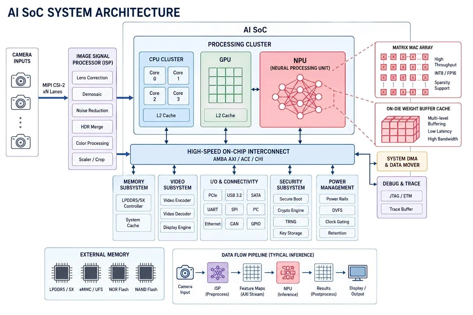
Figure: AI SoC system showing CPU, GPU, and dedicated NPU hardware blocks, with a visual data path running from camera inputs to the NPU matrix accelerator.
Designer Insight: The Reality of Custom SoC Design
Modern SoCs are rarely designed from scratch. Most semiconductor vendors combine licensed IP blocks (such as CPU, GPU, and memory controllers from Arm, Synopsys, or Cadence), custom accelerators, and extensive verification to create application-specific platforms.
How to Select the Right System on a Chip for Your Design
Selecting the correct SoC determines your project's overall power envelope, hardware layout difficulty, and long-term viability. When evaluating silicon, engineers must carefully weigh several key architectural vectors:
- Processing Requirements: Analyze your workload profile. Choose application-class SoCs with a dedicated Memory Management Unit (MMU) if you need to run Linux. Verify that the chip includes an NPU or GPU if you plan to deploy local edge AI or computer vision models.
- Memory and Storage Interfaces: Evaluate whether the SoC requires external LPDDR4/5 memory, which demands high-speed PCB routing with matched-length traces, or if it supports co-packaged DRAM. Ensure the storage bus (such as eMMC or PCIe) meets boot-time and read/write bandwidth criteria.
- Connectivity and I/O Peripherals: Map out your required interfaces. Industrial designs often require CAN-FD and TSN-capable Ethernet. Wearables and mobile IoT devices will require integrated wireless transceivers on-die to avoid the extra cost of external RF chips. Designers can verify physical device package footprints directly within a verified component database.
- Power and Thermal Constraints: Calculate your system's Thermal Design Power (TDP). Low-power IoT nodes must prioritize microamp-tier deep sleep states, whereas multi-GHz application SoCs will require advanced PCB heat spreading, thermal via arrays, or active heatsink cooling. Before finalizing your board layout, submit your requirements to a PCB quotation tool to project fabrication margins.
- Software Ecosystem and BSP Support: Prioritize silicon vendors that provide active board support packages (BSPs), mainlined Linux kernel drivers, and robust SDKs. Bypassing driver development hurdles significantly accelerates your board bring-up schedule.
- Product Lifecycle and Longevity: Ensure the selected SoC vendor provides an official longevity commitment (typically 10 to 15 years for industrial or automotive components) to prevent premature product obsolescence.
Designer Insight: Software Ecosystem of SoC<
When selecting a SoC, hardware specifications are only part of the decision. Software support, BSP quality, Linux kernel maintenance, and long-term component availability often have a greater impact on project success than raw CPU performance.
System on a Chip vs. System on Module vs. System in Package
For projects where custom silicon design is out of reach, hardware designers must choose between packaging and integration form factors:
- System on Module (SoM): A complete computing sub-board integrating the SoC, DRAM, non-volatile storage, and power management onto a pre-verified PCB. This module mounts to a custom carrier board containing application-specific I/O connectors, simplifying high-speed BGA breakouts and DDR memory routing.
- System in Package (SiP): Co-packages multiple individual silicon dies (such as an SoC die alongside discrete LPDDR dies) into a single, unified integrated circuit package, using micro-bumps or silicon interposers to maximize density.
| Attribute | SoC | SiP | SoM |
|---|---|---|---|
| Integration Level | Single die | Multi-die, one package | SoC + support components on sub-board |
| Customizability | Fixed at tapeout | Fixed at packaging | Carrier board is fully custom |
| PCB Layout Complexity | High (BGA breakout, DDR) | High (same as SoC) | Low (carrier board routing only) |
| Time to Market | Longest | Long | Fastest |
| Cost Model | High NRE / Low unit cost | Moderate NRE | Low NRE / Higher unit cost |
| Real-world Example | Snapdragon 8 Elite | Apple M5 package | Variscite VAR-SOM-MX8M-Plus |
By shifting design complexity away from the silicon layout stage, engineering teams can focus on custom carrier boards that are easy to manufacture using optimized assembly workflows.
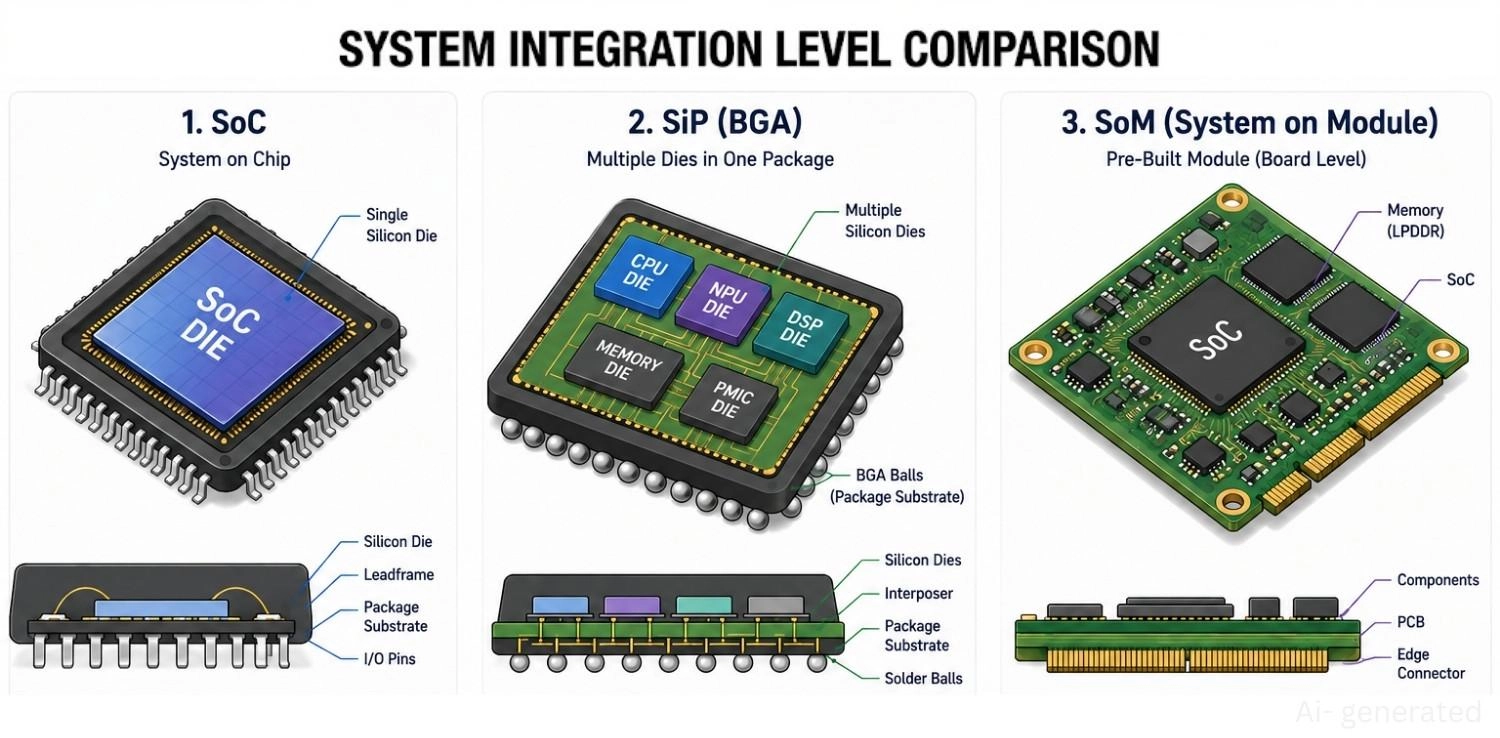
Figure: Structural comparison illustrating die-level (SoC), package-level (SiP), and board-level (SoM) system integration styles.
FAQs About System on a Chip
Q: Is a microcontroller a SoC?
Technically, most microcontrollers qualify as simple SoCs, integrating a CPU, memory, and peripherals on one die. In industry usage, "SoC" typically implies higher integration: multi-GHz application processors, GPU, NPU, and Linux capability. The boundary is a spectrum; Espressif explicitly calls the ESP32-S3 "a low-power MCU-based system-on-chip (SoC)" in its datasheet.
Q: Can a SoC run Linux?
Yes, application-class SoCs with a Cortex-A or equivalent core, an MMU, and sufficient DRAM routinely run Linux. The Broadcom BCM2711 (Raspberry Pi 4), NXP i.MX 8M Plus, TI Sitara AM625, and Qualcomm Snapdragon all run Linux. Microcontroller-class SoCs (ESP32, RP2350) without an MMU cannot run standard Linux.
Q: What is the difference between a SoC and a CPU?
A CPU (Central Processing Unit) is a single processing element - it executes instructions. An SoC integrates a CPU (or multiple CPU cores) alongside GPU, NPU, memory controller, peripherals, and often wireless connectivity on one die. The CPU is merely one block inside the SoC.
Q: Why are SoCs used in smartphones?
Smartphones require the highest compute density, the lowest power consumption, and the smallest PCB footprint of any mass-market product category. Only an SoC integrating CPU, GPU, NPU, ISP, 5G modem, Wi-Fi, and Bluetooth in one 100 square millimeter package can meet those simultaneous constraints.
Q: Is ESP32 a SoC or MCU?
It is both, by definition. Espressif's own datasheet describes the ESP32-S3 as "a low-power MCU-based system-on-chip (SoC)." It integrates CPU cores, Wi-Fi + BLE radio, crypto accelerators, and a ULP coprocessor, yielding SoC-level integration in an MCU-class workflow and price point.
Q: What is the difference between a SoC and a SiP?
An SoC places all functional blocks on a single semiconductor die. A SiP (System in Package) integrates multiple discrete dies, from different processes or vendors, into one package, using wire bonding, flip-chip, or TSV interconnects. An SoC is almost always a SiP once DRAM is co-packaged (as with Apple M5), but not all SiPs contain a single-die SoC.
Conclusion
System on a Chip technology has transformed modern electronics by integrating processors, memory subsystems, communication interfaces, and specialized accelerators into a single device. From IoT sensors and industrial controllers to smartphones and AI edge systems, SoCs provide the performance and efficiency required by today's embedded applications.
Understanding SoC architecture, memory hierarchies, interconnects, and integration trade-offs allows engineers to make better hardware decisions, reduce development risk, and choose platforms that align with long-term product goals.
Popular Articles
• SMD Capacitor Sizes: Complete Size Chart and Selection Tips for PCB Design and Assembly
• SMD Diode Code Lookup: Full List, Marking Guide & Identification [2026 Guide]
• SMD Resistor Package Sizes: Complete Size Chart, Footprints & How to Choose
• SMD Capacitor Codes: Identification, Markings, and Polarity
• How to Solder SMD Components Like a Pro [2026 Updated]
Keep Learning
What Is the ESP32? A Complete Guide to Features, Architecture, Modules, Programming, and Applications
From Wi-Fi-enabled temperature sensors and wearable health monitors to industrial gateways and AI-powered cameras, the ESP32 microcontroller has become one of the world's most widely adopted wireless embedded platforms. Combining a powerful processor with integrated Wi-Fi and Bluetooth, it lets engineers build connected devices without separate networking hardware. This guide covers ESP32 specifications, architecture, the full family of variants, development boards, programming tools, and real-world E......
How to Choose the Right STM32 Microcontroller: Compare Series, Cortex-M Cores, and Key Features
STMicroelectronics ships thousands of STM32 MCU part numbers across more than a dozen series, and that variety is exactly what makes STM32 microcontroller selection difficult. Pick the wrong family, and you pay for it later: oversized BOM cost, wasted power budget, or a board respin when a peripheral turns out to be missing. This STM32 microcontroller selection guide breaks the decision into a five-step framework built on practical engineering criteria, not datasheet marketing copy, so you can match a......
SMD Transistor Code Lookup: Identify Markings, Pinout & Multimeter Test Guide
Repairing a circuit board often brings a familiar frustration: staring at a tiny, three-legged black component with an obscure two- or three-letter code. Whether troubleshooting a bare prototype or a mass-produced PCBA, knowing how to quickly decode these surface-mount device (SMD) markings is an essential skill for any electronics engineer or repair technician. In this comprehensive guide, you will learn: 1. How to decode SMD transistor marking codes 2. How to identify BJT vs MOSFET types 3. How to f......
SMD Capacitor Sizes: Complete Size Chart and Selection Tips for PCB Design and Assembly
In the world of modern electronics, surface mount devices (SMDs) have revolutionized board design, allowing for smaller, faster, and more efficient printed circuit boards. When designing a PCB, selecting the correct SMD capacitor sizes is one of the most critical decisions an engineer must make to ensure both electrical reliability and manufacturability. In this article, you will find practical, authoritative guidance on: Comprehensive SMD capacitor size charts for quick reference. How to read imperia......
SMD Diode Code Lookup: Full List, Marking Guide & Identification [2026 Guide]
In modern electronics, surface-mount diodes are used everywhere - from power input protection circuits to high-speed signal routing. Because these components are extremely small, manufacturers cannot print full part numbers on their bodies. Instead, they use short marking codes such as A2, M7, SS14, or SL, which often confuse beginners during PCB repair, reverse engineering, or component replacement. This guide explains how to decode SMD diode codes, identify polarity, test components using a multimet......
Thin Film vs. Thick Film Resistors: Key Differences & Selection Guide
Key Takeaways Default to thick film resistors for most designs. They are cost-effective, robust, and ideal for pull-ups, LED current-limiting, digital circuits, and surge-prone applications. Choose thin-film resistors whenever a resistor defines an analog quantity, such as a voltage divider, reference network, gain-setting circuit, or current-sensing signal chain. Their tight tolerance and low TCR help maintain measurement accuracy over temperature and time. Most PCB designs use thick film or thin fil......