
What Is System in Package? Architecture, Benefits, and Applications in Modern Electronics
19 min
- What Is System in Package (SiP)?
- How System in Package Works
- Types of System in Package
- Key Components Inside a SiP
- System in Package vs System on Chip
- Key Benefits of System in Package
- Challenges of System in Package
- Applications of System in Package
- System in Package in PCB Design and Assembly
- Future Trends in System in Package
- FAQ About System in Package
- Conclusion
System in Package (SiP) is a semiconductor packaging approach that combines multiple ICs, passive components, and interconnects inside a single package, delivering a complete functional subsystem in the footprint of one component.
SiP has become a foundational technology in smartphones, wireless modules, wearables, and IoT devices. It lets engineers integrate a processor, memory, RF circuitry, and power management into one compact, pre-tested unit, reducing board complexity and shortening time to market.
This guide covers how SiP works, how it compares to System on Chip (SoC), what package types exist, and what engineers need to know about PCB design and assembly when working with SiP modules.
What Is System in Package (SiP)?
A System in Package, a common advanced semiconductor packaging approach also referred to as SiP semiconductor packaging, integrates multiple semiconductor dies and passive components into a single package that functions as a complete subsystem. Unlike a discrete component that handles one task, a SiP module can execute, store, communicate, and manage power, all within the boundaries of one package body.
Key point: SiP is a packaging strategy, not a chip design methodology. It brings separately designed chips together into one package rather than fabricating everything on a single die.
A typical SiP may include any combination of the following:
- Processor or microcontroller (MCU/MPU)
- DRAM or Flash memory
- RF transceiver or modem
- Passive components, such as resistors, capacitors, and inductors
- Power management IC (PMIC)
- MEMS sensors or analog front ends
Because these components are co-packaged with short interconnects, SiP delivers better signal integrity and lower parasitics compared to a multi-chip PCB assembly spread across a larger board area. This matters especially in RF and high-speed digital designs where trace length directly impacts performance.
How System in Package Works
Understanding SiP architecture requires looking at how multiple dies are physically placed, interconnected, and routed within the package boundary.
Multi-Chip Integration
In a SiP, multiple dies are placed either side by side on a common substrate or stacked vertically using advanced bonding techniques. Each die is fabricated independently, often by different foundries using different process nodes, and then assembled at the package level.
This approach is called heterogeneous integration. Because chips do not need to share the same fabrication process, engineers can pair a cutting-edge processor node with mature-node analog circuitry, or combine silicon with compound semiconductors like GaAs for RF applications.
Interconnect Technologies
How dies communicate inside a SiP depends on the package type and performance requirements. Common interconnect methods include:
- Wire bonding: fine gold or copper wires loop from die pads to substrate traces; cost-effective and widely used
- Flip-chip bonding: die is flipped, and solder bumps connect directly to the substrate; shorter paths, better electrical performance
- Through-silicon via (TSV): vertical electrical connections etched through the die itself; enables 3D stacking with minimal path length
- Redistribution layer (RDL): thin-film wiring layer that re-routes die pad locations to match substrate, or other die footprints
Package Substrate and Routing
The substrate serves as the structural backbone and electrical routing layer of a SiP. It carries signal traces between dies, manages power delivery, and provides a thermal conduction path. Substrate quality directly affects signal integrity, power integrity, and EMI performance, meaning substrate-level routing constraints are one of the primary design challenges in complex SiP modules.
Passive and Active Components in SiP
Beyond semiconductor dies, SiP modules typically embed passive components directly into or on top of the substrate. Embedded capacitors reduce supply noise close to the die. Integrated RF filters and matching networks minimize board-level tuning requirements. PMICs manage voltage regulation within the package, reducing the number of external components a PCB designer needs to handle.
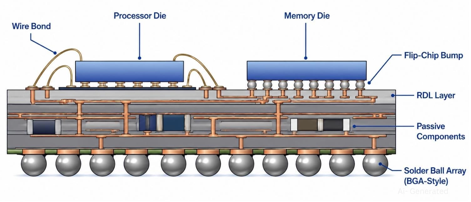
Figure: A System in Package module showing wire-bonded and flip-chip dies alongside passive components on a multilayer substrate with BGA solder ball output.
Types of System in Package
SiP configurations fall into three broad categories based on how dies are arranged spatially. Each has distinct tradeoffs in density, cost, and thermal behavior.
2D SiP
In a 2D SiP, all dies are placed side by side on the same substrate plane. This is the most straightforward configuration to manufacture and validate. Signal paths between dies travel laterally through substrate traces, which keeps interconnect parasitic values manageable.
2D packages are preferred when the die count is low, cost is a priority, or the design involves heterogeneous technologies that cannot be shared on a vertical stack. They remain the dominant configuration in Bluetooth and Wi-Fi module products, frequently utilizing various BGA package types for standard and reliable surface mounting onto the main PCB.
2.5D SiP
2.5D SiP places multiple dies on an interposer, a passive silicon or glass substrate with fine-pitch routing, before mounting the assembly onto the main package substrate. The interposer provides high-density lateral interconnects between dies without requiring TSVs through active silicon.
This configuration is widely used in AI accelerators and high-performance computing (HPC) devices where massive bandwidth between logic and memory dies is required. TSMC's CoWoS platform and AMD's EPYC processor packaging are notable production examples.
3D SiP
3D SiP stacks are stacked vertically, with TSVs providing direct electrical connections between each die. This dramatically reduces the footprint and shortens critical signal paths, but thermal management becomes a significant challenge because heat generated by lower dies must conduct through the stack above.
3D stacking is common in DRAM products such as High Bandwidth Memory (HBM), where multiple DRAM dies are stacked on a logic die to achieve memory bandwidth that flat packages cannot match. Managing thermal resistance and ensuring reliable TSV connections are the primary engineering challenges in 3D SiP design.
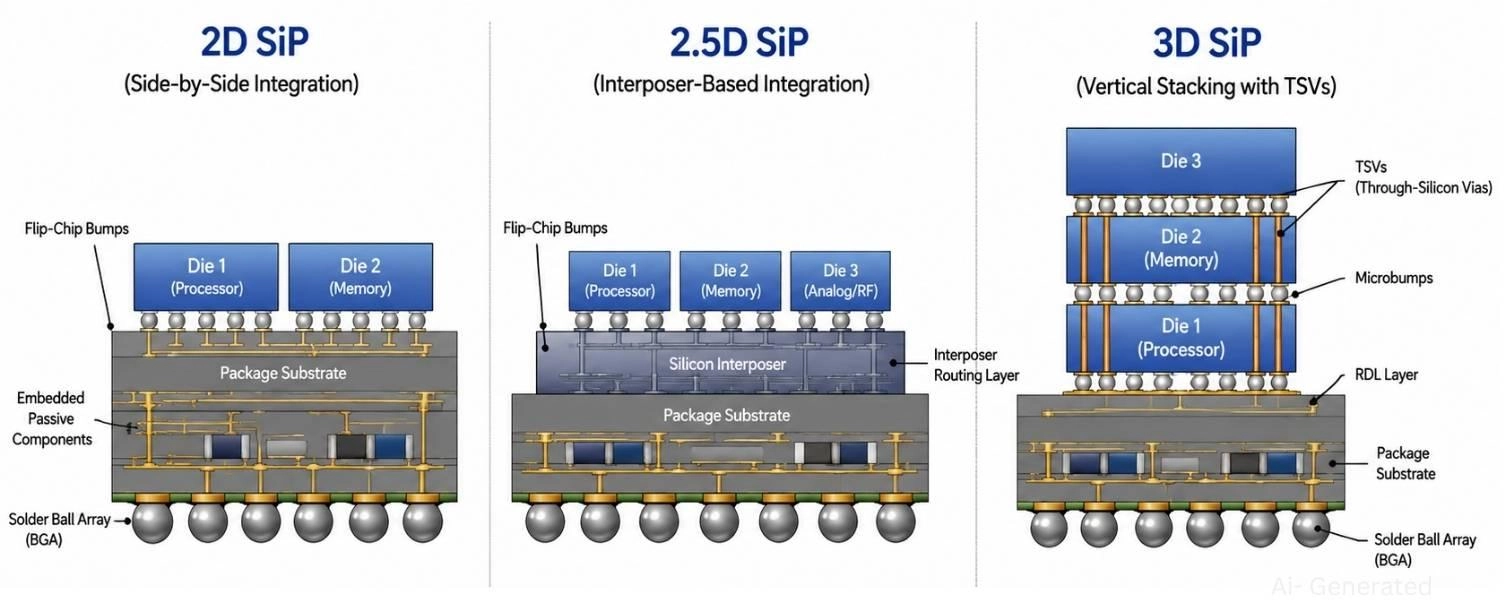
Figure: Comparison of 2D, 2.5D, and 3D System in Package configurations showing die placement, interposer use, and TSV vertical stacking.
Key Components Inside a SiP
Engineers evaluating SiP modules for a design need a clear picture of what each internal component contributes. The following breakdown covers the primary functional blocks found in most SiP products.
Processor / MCU
The processor or microcontroller handles computation and system control. In IoT and wearable SiPs, this is often a low-power ARM Cortex-M core. In mobile or edge AI applications, it may be a high-performance application processor combined with a neural processing unit (NPU). The processor defines the instruction set architecture and dictates the memory interface requirements.
Memory
Most SiP modules include at least one memory type, either SRAM for working memory, NOR Flash for firmware storage, or LPDDR for high-bandwidth applications. Co-packaging memory with the processor eliminates board-level memory routing and reduces signal integrity concerns associated with high-speed memory interfaces such as DDR.
RF Components
RF integration is one of the strongest arguments for choosing SiP over discrete PCB assembly. A typical wireless SiP combines a transceiver, power amplifier, low-noise amplifier (LNA), and RF switch inside the package, with matching networks and filters already tuned. This removes the need for board-level RF layout expertise and reduces the number of iterations for antenna impedance matching.
Key takeaway: SiP reduces board-level RF complexity by moving matching and filtering inside the package.
Passive Components
Decoupling capacitors, filter inductors, and signal termination resistors are co-located with the active dies inside the SiP package. Their proximity reduces supply ripple, decreases EMI, and eliminates the layout-sensitivity that normally comes with placing a bypass capacitor in PCB layout near ICs on your main board.
Power Management IC (PMIC)
Integrating the PMIC inside the SiP simplifies board power architecture. The PMIC generates multiple regulated voltage rails for the processor, memory, and RF subsystems, while keeping power delivery paths short. This is particularly valuable in battery-operated devices where supply efficiency and transient response directly affect runtime.
System in Package vs System on Chip
SiP and SoC are frequently discussed together, but they represent fundamentally different integration strategies. When evaluating the optimal IC package types for a new device, the choice between them affects sourcing, design timelines, and long-term product flexibility.
System on Chip (SoC) integrates all functions onto a single die in one semiconductor process. Every block, including the CPU, memory controller, peripherals, and analog interfaces, shares the same silicon. This delivers excellent area efficiency at high volume, but requires significant NRE investment and locks the design to a single foundry.
System in Package (SiP) takes the opposite approach. Multiple separately designed and tested dies are integrated at the package level alongside passive components. This trades some raw density for design flexibility, faster development cycles, and the ability to combine different process nodes in one module.
Key advantage: SiP allows different chip technologies, such as a 5nm logic die and a mature-node RF chip, to coexist inside one compact package.
| Feature | SiP | SoC |
|---|---|---|
| Integration level | Multi-chip, package-level | Single die, monolithic |
| Design flexibility | High-mix process nodes | Low - one process node |
| Manufacturing complexity | Moderate to high | Very high (leading-edge fab) |
| Time to market | Faster (known-good dies) | Longer (full chip tape-out) |
| Cost (low volume) | Lower | Higher NRE |
| Cost (high volume) | Higher per unit | Lower at scale |
| PCB footprint | Compact | Very compact |
| Upgradability | Easier (replace a die type) | Requires full re-spin |
| Thermal behavior | Moderate challenge | Lower (single die) |
| Heterogeneous integration | Yes | Limited |
When evaluating the two options, the application context is decisive. Neither is universally superior.
SiP is typically the better choice when:
- Heterogeneous integration is required, e.g., combining RF with digital logic
- Rapid prototyping or short development cycles are a priority
- Design reuse across product families is valuable
- RF integration needs to be handled inside the package
SoC is typically preferred when:
- The product is targeting extremely high volumes where NRE amortizes well
- Absolute power efficiency and area density are the primary constraints
- All required functions can be implemented in a single process node
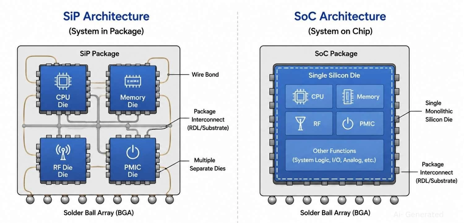
Figure: Comparing System in Package architecture with multiple co-packaged dies versus System on Chip with all functions on a single monolithic die.
Key Benefits of System in Package
The advantages of SiP extend beyond footprint reduction. For engineers designing space-constrained, multi-function products, SiP addresses several interconnected problems simultaneously.
Miniaturization
Combining the processor, memory, RF, and power management into one package removes the routing overhead of board-level connections between these blocks. Smartwatch modules and hearing aid chipsets represent real-world cases where SiP enabled product form factors that would have been physically impossible with discrete component layouts.
Improved Electrical Performance
Short, controlled interconnects within the package reduce parasitic inductance and capacitance. For high-speed digital interfaces and RF circuits, this translates to measurable improvements in signal integrity, reduced noise, and better impedance matching, all without requiring aggressive PCB layout optimization.
Faster Time to Market
SiP modules are typically purchased as pre-integrated, pre-tested subsystems. A design team working with a Wi-Fi/BT SiP module does not need to design the RF front-end, validate the matching network, or certify the radio subsystem independently. Regulatory pre-certification of the module accelerates final product approval.
Heterogeneous Integration
No single fabrication node excels at everything. SiP allows a 5nm logic die to coexist with a 180nm analog die and a GaAs RF chip. This kind of per-function process node optimization is impossible in a monolithic SoC and is one of SiP's most compelling technical differentiators.
Reduced PCB Complexity
Replacing four or five discrete ICs and dozens of passive components with a single SiP module simplifies schematic design, reduces component count, lowers BOM cost, and shrinks the number of placement and soldering operations during assembly. For contract manufacturers, fewer components per board means lower error rates.
Better RF Integration
RF circuits are notoriously sensitive to layout. Placing RF components on a PCB requires careful attention to ground planes, trace impedance, keep-out areas, and coupling paths. A SiP that integrates RF components internally delivers a tested, characterized RF subsystem, so the PCB designer connects an antenna pad, not a full RF circuit.
Key takeaway: With a SiP module, the RF design challenge shifts from board layout to antenna connection, representing a meaningful reduction in design risk.
Challenges of System in Package
SiP is not the right solution for every project. Understanding the limitations helps engineers make an informed decision rather than defaulting to packaging as a shortcut.
Thermal Management
Multiple dies generating heat within a confined package create a thermal concentration problem. In 3D stacks, the die furthest from the package substrate has the highest thermal resistance path. Thermal modeling during the design phase, including thermal simulation of the substrate and package, is essential to avoid junction temperature violations under load.
Testing Complexity
When a fault occurs in a packaged multi-die assembly, isolating it to a specific die is significantly harder than testing discrete components on a PCB. Known-Good Die (KGD) testing before packaging helps catch defects early. Post-package test coverage is more limited, which raises quality-control costs and complicates field failure analysis.
Design Constraints
Substrate routing within a SiP operates under tighter pitch and layer constraints than a PCB. EMI between co-packaged dies must be managed at the substrate level. Design tools for SiP, while maturing, still require specialized expertise compared to standard PCB EDA workflows.
Manufacturing Cost
Advanced packaging requires specialized equipment, precision placement, and tight process controls. Tooling costs are higher than for standard SMT assembly. For low-volume or prototype applications, this cost is typically absorbed by purchasing standard SiP modules rather than designing a custom package, but custom SiP development carries significant NRE.
Applications of System in Package
SiP modules appear across a wide range of industries, from smartphones and mobile devices to industrial sensors, consistently in applications where size, wireless connectivity, or power efficiency are non-negotiable requirements. SiP semiconductor technology has become a standard building block wherever compact integration matters most.
IoT Devices
Industrial and consumer IoT sensors need the smallest possible footprint and the lowest possible power draw. A SiP combining a low-power MCU, LoRa or Zigbee transceiver, and PMIC can deliver a complete wireless node in under 10 mm². Battery life measured in years is achievable when the entire active subsystem is optimized within one package.
Wearables
Smartwatches, fitness trackers, and medical wearables demand high integration in irregular form factors. SiP technology underlies products like the Apple Watch S-series chip, which integrates processor, sensor interfaces, and connectivity in a package small enough to fit inside a watch band module. The SiP approach reduces board layer count and enables slimmer device profiles.
RF and Wireless Modules
Certified Wi-Fi, Bluetooth, and 5G NR modules are among the most commercially mature SiP products available. Module vendors integrate RF front-end components, antenna matching, crystal oscillator, and baseband processing into pre-certified packages. Engineers drop the module onto a carrier board and connect power, GPIO, and an antenna, meaning the RF design work is already done.
The availability of FCC/CE/IC pre-certified SiP modules significantly reduces regulatory burden for product development teams.
Automotive Electronics
Advanced Driver Assistance Systems (ADAS), radar sensors, LiDAR processing units, and V2X communication modules increasingly rely on SiP packaging to meet automotive-grade reliability requirements in compact form factors. The ability to mix mature-node automotive-qualified dies with leading-edge processing dies in one package is a key advantage for automotive SiP.
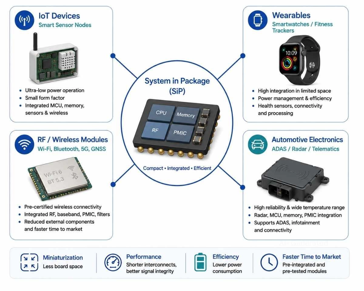
Figure: System in Package modules used in IoT sensor nodes, wearable devices, certified wireless modules, and automotive ADAS electronics.
System in Package in PCB Design and Assembly
Integrating a SiP module onto a PCB requires a different set of design considerations than placing a standard IC. The SiP brings pre-integrated subsystem complexity to the PCB, but the board still needs to be designed correctly to take advantage of it.
When to Choose SiP vs PCB-Based Integration
The choice is not always obvious. The following criteria help frame the decision:
SiP is preferred when:
- Compact board size is a hard constraint, such as in wearables, medical implants, and industrial sensors
- RF integration is required and an off-the-shelf certified module is available
- Time to market is more critical than optimizing per-unit cost
- The design team lacks RF layout expertise
PCB-level discrete integration is preferred when:
- Maximum design flexibility and component substitution are required
- The BOM must be optimized for volume cost with commodity components
- Field repairability or individual chip replacement is a priority
- Thermal management is better handled with board-level heat spreading
PCB Design Considerations for SiP Modules
Designing a PCB for a SiP module requires attention to several areas that differ from standard IC placement. Engineers working with high-density SiP packages should address the following:
Layout and routing:
- Footprint accuracy: use the module manufacturer's land pattern files exactly. Mastering proper solder pad design is critical, as SiP module pads are often non-standard and pitch-sensitive. Errors in the footprint translate directly to assembly yield problems.
- Escape routing: fine-pitch BGA-style SiP modules require careful via arrangement and trace routing to exit the pad array cleanly. Plan for microvia or staggered via strategies on high-density designs.
- Controlled impedance traces: RF signal lines, high-speed data buses, and clock lines require impedance-controlled routing. Define target impedances for relevant nets and confirm stackup capability with your fabrication partner.
Signal, power, and thermal integrity:
- Power integrity: Place decoupling capacitors on each supply pin as close to the pad as placement rules allow. Use short, low-inductance via connections to the power plane.
- Signal integrity: minimize via stubs on high-speed differential pairs. Route differential pairs symmetrically with matched lengths.
- EMI and EMC: provide continuous ground pours under the SiP module. Avoid routing signal traces across ground plane splits in the vicinity of the module.
- Thermal vias: if the SiP module includes an exposed thermal pad, connect it to an internal copper pour or bottom-side copper fill through an array of thermal vias, which is critical for maintaining junction temperatures within spec.
- Power distribution network: model the DC resistance and inductance of power distribution paths from bulk capacitors through vias to the SiP power pins, especially for modules with fast transient loads.
Scaling SiP-Based Designs with JLCPCB Fabrication and Assembly Services
SiP-based PCB designs typically require multilayer board capability, controlled impedance routing, and precise SMT assembly. JLCPCB supports multilayer fabrication with impedance-controlled stackups, which is essential for RF and high-speed SiP interfaces.
For prototypes and production scaling, JLCPCB's PCB Assembly Service handles fine-pitch placement alongside SiP modules, simplifying the transition from fabrication to assembly. Designs with HDI escape routing or BGA-style SiP footprints benefit from the tight dimensional tolerances JLCPCB's fabrication process supports. When building out your BOM, you can also easily source essential components and parts to ensure a smooth transition to manufacturing.
Future Trends in System in Package
Packaging technology is one of the fastest-evolving areas in semiconductor engineering. Several directions will shape how the system in package technology is designed and used over the next decade.
Chiplet Architecture
The chiplet model decomposes a complex SoC into smaller, independently designed functional blocks, called chiplets, that are then integrated using advanced packaging. Intel's Foveros, AMD's 3D V-Cache, and TSMC's SoIC platforms are early production examples.
Chiplet-based SiP lets vendors mix best-in-class IP blocks from different suppliers, enabling faster iteration and reducing the design risk tied to large monolithic die development.
AI and Edge Computing
Edge AI hardware must deliver high compute density within tight power and space limits. SiP enables close integration of a neural processing unit (NPU) with high-bandwidth memory (HBM or LPDDR5X) and communication interfaces, reducing memory access latency and improving energy efficiency.
Wearable and embedded AI devices will increasingly depend on SiP packaging for this reason.
Advanced Packaging Technologies
Fan-out wafer-level packaging (FOWLP) removes the organic substrate layer, enabling finer RDL routing and thinner package profiles. Hybrid bonding, which involves direct copper-to-copper die interconnects, promises a density an order of magnitude higher than flip-chip technology.
Together, these advances will push SiP performance closer to monolithic SoC integration while retaining the heterogeneous integration flexibility SiP is known for.
FAQ About System in Package
Q: Can System in Package reduce PCB layer count?
Yes. Consolidating components into one module eliminates dense inter-chip routing, often reducing required board layers (e.g., from 8 to 4).
Q: Why is thermal management challenging in 3D SiP?
Vertical die stacking increases thermal resistance. Heat concentrates in a confined column rather than spreading laterally, making thermal simulation critical.
Q: Are SiP modules pre-certified for wireless communication?
Many commercial wireless SiPs include FCC, CE, and IC pre-certifications. This narrows the end-product testing scope, though datasheet verification is required.
Q: What is the difference between SiP and a multi-chip module (MCM)?
An MCM simply groups chips for density. A SiP integrates a complete, application-optimized functional subsystem, including passives and power management.
Q: Is SiP suitable for RF and high-frequency applications?
Yes. Internal RF integration eliminates board-level impedance and routing issues, leaving only a simple antenna pad connection for the host PCB.
Q: Can SiP simplify PCB assembly?
Yes. Replacing discrete components with one SiP reduces BOM count, solder joints, and placement operations, lowering assembly defects and cycle times.
Q: Are SiP modules repairable or upgradeable?
Generally no. A single internal failure requires replacing the entire module, making discrete components better for field repairability.
Q: What PCB design considerations are most important for SiP modules?
Top priorities are using exact land patterns, routing controlled impedance, placing thermal via arrays under exposed pads, and positioning decoupling capacitors near supply pins.
Conclusion
System in Package (SiP) enables engineers to integrate processing, memory, RF, and power management into compact, high-performance modules that simplify modern electronic design. As devices continue to shrink while demanding more functionality, SiP remains a key solution for IoT, wireless, wearable, and automotive applications.
Popular Articles
• SMD Diode Code Lookup: Full List, Marking Guide & Identification [2026 Guide]
• SMD Resistor Package Sizes: Complete Size Chart, Footprints & How to Choose
• SMD Capacitor Codes: Identification, Markings, and Polarity
• SMD Capacitor Sizes: Complete Size Chart and Selection Tips for PCB Design and Assembly
• How to Solder SMD Components Like a Pro [2026 Updated]
Keep Learning
PoP Package (Package on Package) Explained: Architecture, Assembly, and SMT Challenges
In the race for miniaturization, fitting more processing power into smaller footprints is the ultimate challenge for PCB designers. Package on Package (PoP) technology answers this by integrating logic and memory vertically, becoming the standard for modern mobile processors. However, this 3D architecture demands advanced SMT assembly capabilities beyond standard fabrication. JLCPCB specializes in the high-precision manufacturing required to master these complex stacks. This guide covers how PoP packa......
What Is a PQFP Package? Plastic Quad Flat Package Design, Footprint, and Assembly Guide
The Plastic Quad Flat Package (PQFP) is a widely used IC package in industrial, automotive, and embedded designs. This article provides a practical, engineering-focused guide to PQFP package. It explains how PQFP is built, when it makes sense to use it, how it compares with newer package types, and what designers should consider in terms of footprint design, thermal performance, signal integrity, manufacturing, and reliability. What Is a PQFP Package (Plastic Quad Flat Package)? A Plastic Quad Flat Pa......
Small Outline Integrated Circuit (SOIC): Package, Specs & Uses
As designs transition from legacy through-hole components to high-density Surface Mount Technology (SMT), the Small Outline Integrated Circuit (SOIC) remains the industry standard for operational amplifiers, flash memory, sensors, and microcontrollers. It stands as a testament to balanced engineering, offering a perfect compromise between the miniaturisation demanded by modern consumer electronics and the ruggedness required for industrial applications. This article serves as a definitive engineering ......
A Complete Guide to Surface Mount Device (SMD)
Imagine holding a smartphone in your hand. Inside that sleek device lies a complex network of thousands of miniature components — resistors smaller than a grain of rice, capacitors thinner than a fingernail, and integrated circuits containing millions of transistors. Without Surface Mount Technology (SMT) and its compact Surface Mount Devices (SMDs), none of this would exist. Just a few decades ago, electronics were bulky. Radios filled desks, computers filled rooms, and assembling a circuit meant dri......
Circuit Breaker Types Explained: MCB, MCCB, RCCB, RCBO, ACB, VCB & SF6 Circuit Breakers
A circuit breaker automatically disconnects power when it detects faults such as overloads or short circuits, protecting equipment and reducing fire risk. Different circuit breaker types are designed for different voltage levels, current ratings, and applications, from household distribution boards to high-voltage substations. This guide explains the most common types - including MCBs, MCCBs, RCCBs, RCBOs, ACBs, VCBs, and SF6 breakers and helps you choose the right one for your application. Figure: Ci......
Quad Flat Package (QFP): The Engineer's Guide to Design, Assembly and Thermal Management
What is QFP Package? The Quad Flat Package (QFP) is one of the most popular surface mount technology (SMT) package formats throughout the history of electronic manufacturing. After it became standard in the 1980s, the QFP has been the industry standard for integrated circuits (ICs) with moderate to high pin counts that typically range from 32 to 304 pins, so it was a good alternative for simple SOIC packages and complex Ball Grid Arrays (BGAs) at the same time. Defined by its "gull-wing" leads extendi......