
The Ultimate Guide to SMD Transistor Package: Sizes, Footprints, Thermal Performance & Selection
18 min
- SMD Transistor Package Chart
- Common SMD Transistor Package Types
- SOT-23 vs SOT-223 vs SOT-323: Key Differences
- How to Choose the Right SMD Transistor Package
- Why SMD Transistor Package Sizes Matter
- What Is an SMD Transistor Package?
- Understanding SMD Transistor Naming and Codes
- FAQs About SMD Transistor Sizes
- Conclusion
Choosing the wrong transistor package, thermal limitations, or excessive PCB area quickly becomes a problem. SMD transistor packages range from compact SC-70 and SOT-523 devices to much larger DPAK and D2PAK power packages, each optimized for different current, thermal, and assembly requirements.
This guide compares common SMD transistor package sizes, including SOT-23, SOT-89, SOT-223, SC-70, DPAK, and D2PAK.
You'll find nominal dimensions, footprint sizes, thermal characteristics, current capabilities, and guidance on choosing the right package for PCB layout, prototyping, and production assembly.
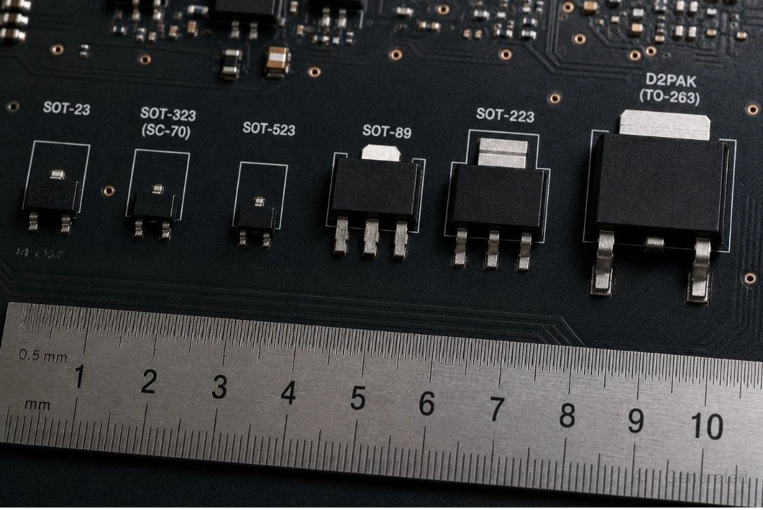
Figure: Various SMD transistor packages on a PCB alongside a precision ruler to show relative scale from SC-70 to D2PAK.
SMD Transistor Package Chart
| Package | Nominal Package Size (with leads) | PCB Footprint Span | Typical Current | Thermal Performance | Common Use |
|---|---|---|---|---|---|
| SOT-523 | ~1.6 × 1.6 mm | 1.8 × 1.8 mm | <200 mA | Poor | Wearables, mobile |
| SC-70 / SOT-323 | ~2.0 × 2.1 mm | 2.1 × 2.8 mm | <600 mA | Poor | Consumer electronics, RF |
| SOT-23 | ~2.9 × 2.4 mm | 3.1 × 3.3 mm | <600 mA | Poor–Fair | General switching, amplifiers |
| SOT-89 | ~4.5 × 4.0 mm | ~4.7 × 5.4 mm | ~1 A | Good | RF amps, LDOs, switching |
| SOT-223 | ~6.5 × 7.0 mm | 6.7 × 8.1 mm | 1–2 A | Good (with copper pour) | LDOs, medium-power |
| DPAK (TO-252) | ~6.6 × 10.0 mm | 6.6 × 11.2 mm | 3–10 A | Good–Excellent | Regulators, motor drivers |
| D2PAK (TO-263) | ~10.2 × 15.0 mm | 10.4 × 17.0 mm | Tens of A (varies) | Excellent | Power MOSFETs, industrial |
Common SMD Transistor Package Types
Note
Dimensions listed below are overall nominal package sizes, including leads. Exact values may vary slightly between manufacturers and JEDEC variants. Always verify against device-specific datasheets.
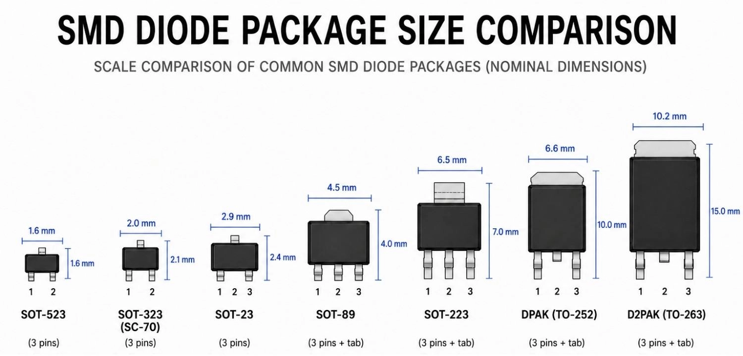
Figure: Seven SMD transistor packages from smallest to largest: SC-70, SOT-523, SOT-323, SOT-23, SOT-223, DPAK, and D2PAK, each labeled with nominal dimensions.
SOT-23
Nominal Package Size (w/ leads): ~2.9 × 2.4 mm | Typical Footprint Span: 3.1 × 3.3 mm
The most common SMD transistor package across general electronics. Three leads (emitter, base, collector or source, gate, drain) with enough pad area for reliable hand soldering.
- Used for: signal switching, level shifting, small logic MOSFETs, amplifiers
- Current: up to ~600 mA depending on device
- Good balance of size, solderability, and availability; ideal for prototyping
SOT-323 (SC-70)
Nominal Package Size (w/ leads): ~2.0 × 2.1 mm | Typical Footprint Span: 2.1 × 2.8 mm
Electrically identical pinout to SOT-23, physically smaller overall span. Common in consumer electronics where board density matters more than manual rework capability.
- Used for: compact switching circuits, RF front-end components, mobile devices
- Harder to hand-solder than SOT-23; bridging risk is higher
- SC-70 is the JIS designation for the same package
SC-70
SC-70 is the JIS designation commonly used for the SOT-323 package family. The two names are often used interchangeably, depending on manufacturer documentation. See SOT-323 above for dimensions and applications.
SOT-89
Nominal Package Size (w/ leads): ~4.5 × 4.0 mm | Typical Footprint Span: ~4.7 × 5.4 mm
A very popular medium-power package that bridges the gap between SOT-23 and SOT-223. The footprint spans up to 5.4 mm vertically to allow proper solder fillets for its extended center tab and downward-facing pins.
- Used for: Medium-power RF amplifiers, LDO voltage regulators, and power switches
- Thermal Performance: Excellent for its size when the center tab is soldered to a copper pour
- Lies flat on the PCB, making it highly robust against physical vibration
SOT-523
Nominal Package Size (w/ leads): ~1.6 × 1.6 mm | Typical Footprint Span: 1.8 × 1.8 mm
Ultra-miniature package, significantly reducing the required PCB footprint. Used almost exclusively in wearables and mobile devices, where board space is critically constrained.
- Low-current applications only (typically under 200 mA)
- Automated assembly strongly recommended; microscope inspection required for rework
- Not suitable for manual prototyping
SOT-223
Nominal Package Size (w/ leads): ~6.5 × 7.0 mm | Typical Footprint Span: 6.7 × 8.1 mm
Larger than it looks in datasheets. The extended thermal tab is what makes this package useful. Available in 3-pin and 4-pin variants.
- Used for: LDO voltage regulators, medium-power BJTs and MOSFETs, current sources
- The thermal tab must be soldered to a copper pour for full thermal benefit
- One of the easiest SMD transistor packages to hand-solder
TO-252 (DPAK)
Nominal Package Size (w/ leads): ~6.6 × 10.0 mm | Typical Footprint Span: 6.6 × 11.2 mm
The standard mid-range power package. Large exposed pad on the bottom transfers heat directly into the board's copper.
- Used for: switching regulators, motor driver transistors, automotive electronics
- Handles up to several tens of amps continuous with appropriate PCB thermal design
- Often requires thermal vias under the pad for multi-layer boards
TO-263 (D2PAK)
Nominal Package Size (w/ leads): ~10.2 × 15.0 mm | Typical Footprint Span: 10.4 × 17.0 mm
The largest common SMD power transistor package. Pin-compatible with TO-220 through-hole in many cases, but surface-mount.
- Used for: high-current MOSFETs, DC-DC converters, industrial and automotive power stages
- Large copper area required for thermal management; reflow soldering strongly preferred
- Not a small-board package; plan layout accordingly
DFN and QFN Leadless Transistor Packages
Leadless packages with exposed thermal pads. No leads extend past the body outline. Common in modern power electronics, where both size and inductance matter.
- Very low parasitic inductance: advantageous at switching frequencies above a few MHz
- Excellent thermal performance via a large exposed bottom pad
- Standard DFN2 for small transistors: ~1.0 x 0.6 mm; larger variants up to 3 x 3 mm for power devices
- Require reflow or hot-air soldering; not hand-solderable
SOT-23 vs SOT-223 vs SOT-323: Key Differences
Physical Size Comparison
| Package | Package Size (w/ leads) | PCB Footprint Span | Lead Pitch |
|---|---|---|---|
| SOT-323 | ~2.0 × 2.1 mm | 2.1 × 2.8 mm | 0.65 mm |
| SOT-23 | ~2.9 × 2.4 mm | 3.1 × 3.3 mm | 0.95 mm |
| SOT-223 | ~6.5 × 7.0 mm | 6.7 × 8.1 mm | 2.30 mm |
SOT-323 is not simply a "small SOT-23". The lead pitch changes, so the footprints are not interchangeable without PCB modifications.
Power Handling Differences
- SOT-323 / SOT-23: similar thermal performance; both are limited to low-power applications under 500 mW continuous without heat spreading.
- SOT-223: the exposed thermal tab is a step change in capability; attached to copper, it can dissipate 1-2 W continuously.
- θJA drops from ~300°C/W (SOT-23) to ~100°C/W (SOT-223 with copper pour).
Thermal Dissipation Capability
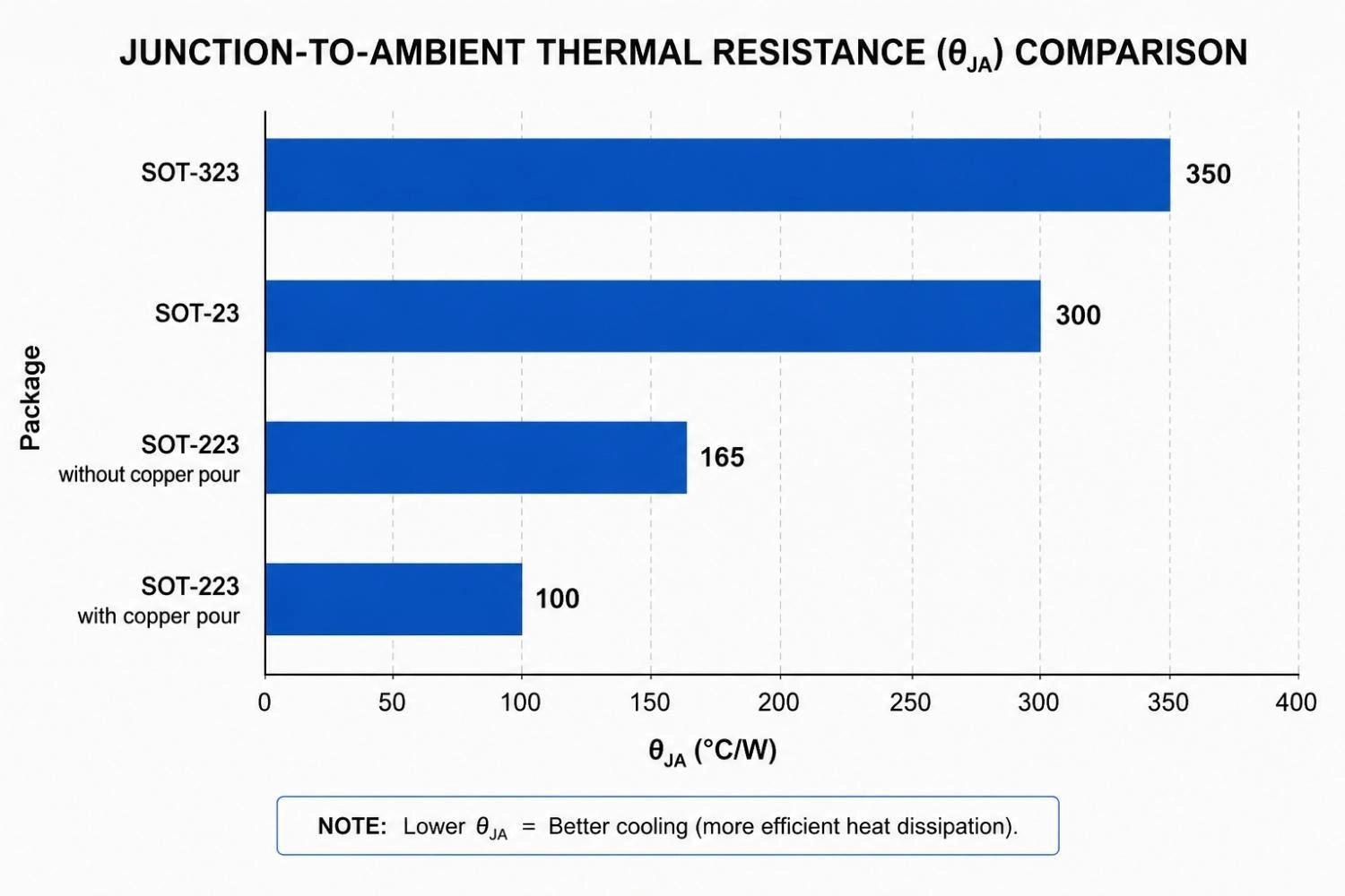
Figure: Horizontal bar chart comparing thermal resistance values for SOT-323, SOT-23, SOT-223 without copper pour, and SOT-223 with copper pour - illustrating the cooling advantage of the SOT-223 thermal tab.
Typical Use Cases
| Package | Best For |
|---|---|
| SOT-323 | Compact low-current switching; dense consumer PCBs |
| SOT-23 | General-purpose BJT/MOSFET switching; prototyping |
| SOT-223 | LDO regulators; medium-power transistors; anything needing >500 mW |
Which Package Should You Choose?
- Tight board space, low current → SOT-323 or SC-70
- General-purpose prototyping → SOT-23; good availability, hand-solderable, wide device selection
- Need more than 500 mW dissipation → SOT-223 minimum; pair with a copper pour
- Replacing a TO-92 on an SMD board → SOT-23 is the closest direct equivalent
How to Choose the Right SMD Transistor Package
SMD Transistor For Low-Power Signal Circuits
Recommended: SOT-523, SC-70 / SOT-323
- Logic-level switching under 100 mA
- Sensor interfaces and signal conditioning
- Low-noise amplifiers in space-constrained layouts
Use SOT-523 or SC-70 / SOT-323 only if automated assembly is confirmed. Manual rework of the SOT-523 package in production is not practical.
SMD Transistor For Switching Regulators and Power MOSFETs
Recommended: SOT-89, SOT-223, DPAK, D2PAK
- Copper pour under the thermal tab is not optional for these applications; it's required to reach the rated current.
- Add thermal vias (0.3-0.4 mm drill, ~4-9 vias) below the exposed pad on multilayer boards.
- For continuous currents above 5 A, D2PAK with adequate copper spreading is the practical minimum.
SMD Transistor For RF and High-Frequency Applications
- SOT-323 and SC-70 have shorter bond wires and lower parasitic inductance than SOT-23.
- DFN/QFN packages perform best above ~100 MHz due to near-zero lead inductance.
- RF transistors above a few GHz often come in proprietary micro packages; don't assume standard footprint compatibility.
SMD Transistor For Heat-Sensitive Designs
- Maximize copper pour area: a 1 cm² pour can drop ፀJA by 30-50°C/W for packages with exposed pads like SOT-89 and DPAK.
- Add a thermal relief break between the transistor's thermal pad and nearby sensitive components.
- If junction temperature calculations push close to maximum limits, step up one package size rather than chasing complex thermal management.
SMD Transistor For Compact IoT and Wearable Devices
- SC-70 / SOT-323 and SOT-523 are the typical choices for transistor switching in wearable designs.
- Battery-powered designs benefit from lower RDS(on) MOSFETs in small packages over BJTs, with less quiescent loss.

-
Assembly precision for these packages (0.65 mm pitch and below) requires a well-calibrated SMT line; JLCPCB's PCB assembly service supports fine-pitch miniature packages as part of standard production.
Why SMD Transistor Package Sizes Matter
Impact on PCB Space and Compact Designs
Package size directly determines how tightly you can route a board. In IoT sensors, wearables, and portable devices, every square millimeter counts. Choosing a smaller package like SOT-523 can free up real estate for passives, connectors, or battery area.
That said, shrinking the package doesn't come free:
- Smaller packages reduce board area but limit heat spreading and complicate manual assembly.
- Larger packages like DPAK and D2PAK take more space but handle thermal loads that would exceed the thermal capability of a SOT-23.
- Ultra-small packages (SOT-523) practically require automated pick-and-place; hand soldering them is error-prone even with magnification.
For dense two-layer boards in consumer electronics, SOT-323 is often the sweet spot. For power stages in motor controllers or DC-DC converters, larger power packages become more appropriate.
Power Dissipation and Thermal Performance
Every transistor in operation generates heat proportional to its power dissipation. The exact formula depends on whether you are utilizing a BJT or MOSFET in your circuit design:
PD = VCE x IC (BJT) or PD = ID² x RDS(on) (MOSFET)
How well the package sheds that heat depends on its thermal resistance (junction to ambient). A lower thermal resistance means cooler operation at the same power level.
| Package | Typical Thermal Resistance (C/W) |
|---|---|
| SOT-23 | ~300 |
| SOT-89 | ~150 |
| SOT-223 | ~100 |
| DPAK (TO-252) | ~60-80 |
| D2PAK (TO-263) | ~40-50 |
SOT-23 simply doesn't have the copper contact area to handle anything beyond a few hundred milliwatts continuously.
SOT-89 and SOT-223's exposed thermal tabs change this significantly; attach it to a copper pour, and it behaves much closer to a small power package.
DPAK and D2PAK are proper power packages: their exposed pads are designed to transfer heat directly into the board copper.
Current Handling Capability vs Package Size
Current capability scales roughly with package size because bigger pads mean more copper, more thermal mass, and lower resistance in the current path.
- SOT-523 → typically under 200 mA continuous; logic switching only
- SOT-23 → up to ~600 mA depending on the device; signal switching, small MOSFETs
- SOT-89 → up to ~1 A; excellent for medium-power RF and LDOs
- SOT-323(SC-70) → similar to SOT-23 in current capacity, smaller footprint
- SOT-223 → up to ~1-2 A with adequate copper; LDO regulators, medium-power switching
- DPAK / D2PAK → up to several tens of amps depending on device and PCB thermal design; power stages, motor drivers, regulators
Always cross-check the device datasheet, as package current limits and transistor ratings interact. A 10 A MOSFET in a DPAK package might be thermally limited to 5 A without a heatsink copper pour.
Assembly, Soldering, and Manufacturing Considerations
Proper reflow soldering handles all SMD transistor packages cleanly with an appropriate stencil design. The issues arise outside of automated assembly:
- SOT-23: manageable with fine-tip iron and flux; prototyping-friendly.
- SC-70 / SOT-323: difficult to hand-solder; the 0.65 mm pitch increases bridging risk, making magnification necessary.
- SOT-523: pads are so close together (0.5 mm pitch) that hand soldering almost always produces bridging; automated assembly is strongly preferred.
- SOT-89, SOT-223: easy to hand-solder due to large pads and exposed tabs.
- DPAK / D2PAK: the exposed pad needs solid solder contact for thermal performance, which is hard to achieve reliably by hand; reflow recommended.
Note
For production runs, JLCPCB's PCB assembly services handle the full range from SC-70 to D2PAK without issue. If you're prototyping with ultra-small packages, it's worth ordering assembled boards rather than fighting with tweezers and hot air.
What Is an SMD Transistor Package?
Difference Between Package and Transistor Type
The package is the physical housing: the plastic body, lead frame, and pad geometry. The transistor type (BJT, MOSFET, JFET) is the semiconductor inside. These are independent: the same transistor die is often available in multiple packages.
For example:
- A common NPN BJT like the 2N3904 comes in SOT-23, TO-92 (through-hole), and SOT-323.
- Power MOSFETs ship in SOT-23 for low-power variants, DPAK for mid-power, and D2PAK for high-power.
When you're searching for a replacement or substitute, the package affects your footprint, not the electrical behavior.
SMD vs Through-Hole Transistor Sizes
| Through-Hole | SMD Equivalent | Difference |
|---|---|---|
| TO-92 | SOT-23 | ~4x smaller footprint |
| TO-220 | D2PAK (TO-263) | Similar thermally, SMD saves vertical height |
| TO-92 | SC-70 | ~6-8x smaller footprint |
When evaluating surface-mount vs. through-hole layout options, remember that SMD packages sit flush on the board, enabling automated assembly and eliminating lead-forming steps. Through-hole packages remain useful for hand-built prototypes and high-vibration environments where solder joint mechanical strength matters.
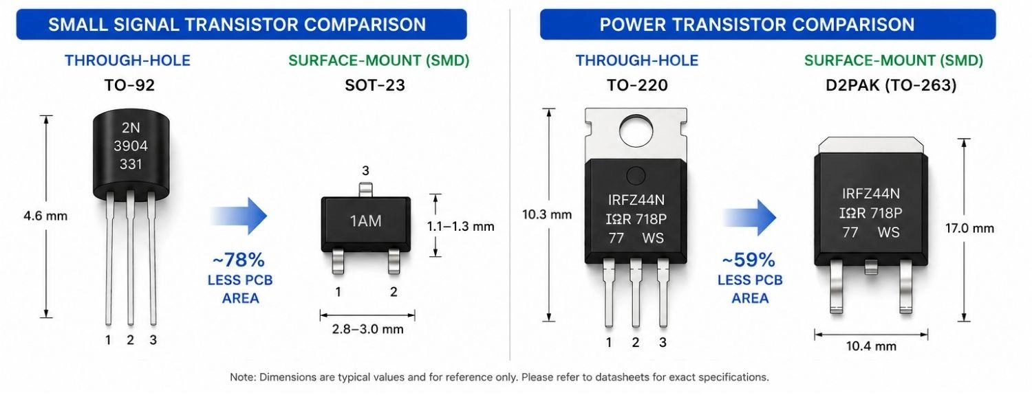
Figure: The size reduction from a TO-92 through-hole package to a SOT-23 SMD package, and a TO-220 to a D2PAK.
Common Package Naming Systems (TO, SOT, SC Packages)
- TO (Transistor Outline): JEDEC-originated; includes TO-92 (THT), TO-252 (DPAK), TO-263 (D2PAK)
- SOT (Small Outline Transistor): broad family covering SOT-23, SOT-89, SOT-223, SOT-323, SOT-523
- SC (Small Circuit): used mainly in JIS/EIAJ naming; SC-70 is widely used in datasheets alongside SOT-323
Note: manufacturers don't always agree on naming. SOT-323 and SC-70 refer to packages of nearly identical dimensions but are listed under different designations depending on the manufacturer. Always verify footprint dimensions against the specific datasheet before placing parts.
SMD Transistor Package Footprint Comparison
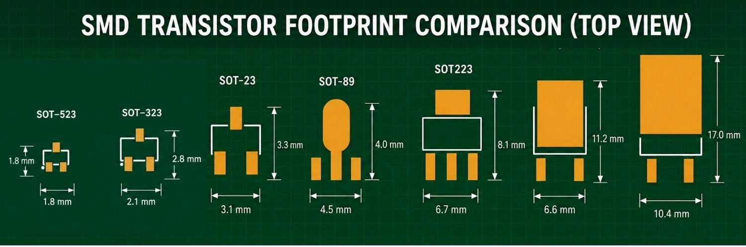
Figure: Top-down footprint comparison of six SMD transistor packages on a 1 mm PCB grid, showing relative pad sizes and footprint areas from SOT-523 to D2PAK.
Smallest SMD Transistor Packages
- SOT-523: Requires a tiny 1.8 × 1.8 mm footprint span; requires automated assembly.
- SC-70 / SOT-323: Requires a 2.1 × 2.8 mm footprint span; difficult but possible to hand solder with magnification.
- DFN ultra-small: down to 1.0 × 0.6 mm; leadless, board-level inspection needs X-ray or optical microscopy.
For wearable designs using these packages, validate your paste stencil thickness and aperture size. Bridging and insufficient solder are the most common failure modes.
Largest Power Transistor SMD Packages
- D2PAK (TO-263): Takes up a massive 10.4 × 17.0 mm footprint span; effectively a surface-mount TO-220.
- DPAK (TO-252): Mid-range power taking a 6.6 × 11.2 mm footprint span; good thermal performance without the D2PAK's board area demand.
- Both require adequate copper pours (typically 1–2 cm² minimum for full rated current) and thermal via arrays for inner-layer heat spreading on multilayer boards.
Understanding SMD Transistor Naming and Codes
Understanding SOT Package Naming
SOT numbering is not strictly sequential by size:
- SOT-523 → 3-lead, ultra-miniature package
- SOT-323 → 3-lead, smaller than SOT-23
- SOT-23 → 3-lead, standard general-purpose size
- SOT-89 → 3-lead + tab, medium power
- SOT-223 → 4-lead (3 + exposed tab), largest of the common SOTs
The number doesn't reliably indicate size. Always check actual dimensions.
JEDEC Package Standards
JEDEC standardizes package outlines so that a footprint from one supplier fits a device from another. In practice, there are minor variations in pad dimensions and tolerances between manufacturers, so always verify the recommended land pattern and package dimensions against the specific transistor datasheet before PCB layout. Understanding transistor package dimensions also helps when selecting compatible SMD diode footprints and MOSFETs on mixed-signal PCBs. Component availability and package variants can also be checked through JLCPCB Parts before finalizing your design.
SMD Transistor Marking Codes
SMD transistor bodies are too small for full part numbers, so manufacturers laser-print abbreviated 2–3 character codes. Because the same code can represent completely different devices from different manufacturers, relying on the marking alone without knowing the physical package size leads to misidentification.
If you need to identify an unknown component based on its markings, check out our comprehensive guide on how to read SMD transistor codes for detailed lookup tables and identification strategies.
FAQs About SMD Transistor Sizes
Q: What is the most widely used surface-mount transistor package in PCB design?
The SOT-23 package serves as the industry standard for general-purpose surface-mount transistors. It is highly favored because it balances a compact 3.1 × 3.3 mm footprint span with enough surface area for reliable hand soldering during hardware prototyping.
Q: Are there SMD transistor sizes smaller than the standard SOT-23?
Yes. Packages like the SOT-323 (2.1 × 2.8 mm footprint span) and SOT-523 (1.8 × 1.8 mm footprint span) are designed for ultra-dense PCBs. For even smaller footprints, leadless DFN packages offer extreme miniaturization but require automated SMT lines for assembly.
Q: Which surface-mount transistor package is best for high-power applications?
The D2PAK (TO-263) package is generally the most capable standard SMD housing for high-current loads. When paired with a properly designed thermal copper pour on the PCB spanning its 10.4 × 17.0 mm footprint, it can manage several tens of amps, making it ideal for motor drivers and power stages.
Q: Is the TO-236 package identical to the SOT-23 footprint?
TO-236 is simply a JEDEC alternative designation for the classic SOT-23 package. While they are dimensionally equivalent, it is always recommended to verify land patterns against the specific component datasheet before routing your board.
Q: How can I accurately identify an unknown surface-mount transistor component?
You must combine physical measurements with marking codes. Measure the body dimensions and lead pitch with calipers to confirm the exact package type (e.g., SOT-323 vs SOT-23). Then, use the laser-etched marking code to cross-reference an SMD component database for the specific part number.
Q: Which SMD transistor package type is easiest to solder by hand?
The SOT-223 package is widely considered the easiest to work with manually. Its larger body size, wide 2.3 mm lead pitch, and extended thermal tab make alignment straightforward without requiring a microscope.
Conclusion
SMD transistor package selection comes down to three variables working against each other: board space, thermal headroom, and assembly complexity.
SOT-23 covers most general-purpose use cases. SOT-323 or SC-70 are required when space is tight and current is low.
SOT-223 is the minimum threshold for reliably dissipating anything over 500 mW, while DPAK and D2PAK remain essential for true power electronics.
Building a PCB with miniature or power SMD transistor packages? JLCPCB supports comprehensive SMT assembly from compact SC-70 devices to high-current D2PAK power stages, for both prototyping and production. Verify package footprints and component availability through JLCPCB Parts before finalizing your PCB layout. Ready to manufacture? Get an instant estimate on our quotation page.
Popular Articles
• SMD Capacitor Sizes: Complete Size Chart and Selection Tips for PCB Design and Assembly
• SMD Diode Code Lookup: Full List, Marking Guide & Identification [2026 Guide]
• SMD Resistor Package Sizes: Complete Size Chart, Footprints & How to Choose
• SMD Capacitor Codes: Identification, Markings, and Polarity
• How to Solder SMD Components Like a Pro [2026 Updated]
Keep Learning
What Is the ESP32? A Complete Guide to Features, Architecture, Modules, Programming, and Applications
From Wi-Fi-enabled temperature sensors and wearable health monitors to industrial gateways and AI-powered cameras, the ESP32 microcontroller has become one of the world's most widely adopted wireless embedded platforms. Combining a powerful processor with integrated Wi-Fi and Bluetooth, it lets engineers build connected devices without separate networking hardware. This guide covers ESP32 specifications, architecture, the full family of variants, development boards, programming tools, and real-world E......
How to Choose the Right STM32 Microcontroller: Compare Series, Cortex-M Cores, and Key Features
STMicroelectronics ships thousands of STM32 MCU part numbers across more than a dozen series, and that variety is exactly what makes STM32 microcontroller selection difficult. Pick the wrong family, and you pay for it later: oversized BOM cost, wasted power budget, or a board respin when a peripheral turns out to be missing. This STM32 microcontroller selection guide breaks the decision into a five-step framework built on practical engineering criteria, not datasheet marketing copy, so you can match a......
SMD Transistor Code Lookup: Identify Markings, Pinout & Multimeter Test Guide
Repairing a circuit board often brings a familiar frustration: staring at a tiny, three-legged black component with an obscure two- or three-letter code. Whether troubleshooting a bare prototype or a mass-produced PCBA, knowing how to quickly decode these surface-mount device (SMD) markings is an essential skill for any electronics engineer or repair technician. In this comprehensive guide, you will learn: 1. How to decode SMD transistor marking codes 2. How to identify BJT vs MOSFET types 3. How to f......
SMD Capacitor Sizes: Complete Size Chart and Selection Tips for PCB Design and Assembly
In the world of modern electronics, surface mount devices (SMDs) have revolutionized board design, allowing for smaller, faster, and more efficient printed circuit boards. When designing a PCB, selecting the correct SMD capacitor sizes is one of the most critical decisions an engineer must make to ensure both electrical reliability and manufacturability. In this article, you will find practical, authoritative guidance on: Comprehensive SMD capacitor size charts for quick reference. How to read imperia......
SMD Diode Code Lookup: Full List, Marking Guide & Identification [2026 Guide]
In modern electronics, surface-mount diodes are used everywhere - from power input protection circuits to high-speed signal routing. Because these components are extremely small, manufacturers cannot print full part numbers on their bodies. Instead, they use short marking codes such as A2, M7, SS14, or SL, which often confuse beginners during PCB repair, reverse engineering, or component replacement. This guide explains how to decode SMD diode codes, identify polarity, test components using a multimet......
Thin Film vs. Thick Film Resistors: Key Differences & Selection Guide
Key Takeaways Default to thick film resistors for most designs. They are cost-effective, robust, and ideal for pull-ups, LED current-limiting, digital circuits, and surge-prone applications. Choose thin-film resistors whenever a resistor defines an analog quantity, such as a voltage divider, reference network, gain-setting circuit, or current-sensing signal chain. Their tight tolerance and low TCR help maintain measurement accuracy over temperature and time. Most PCB designs use thick film or thin fil......