Rigid Flex Circuit: A Complete Guide to Design, Manufacturing, and Applications
15 min
- Understanding Rigid Flex Circuits
- Design Considerations for Reliable Rigid Flex Circuits
- Typical Applications of Rigid Flex Circuits
- Rigid Flex Circuit Manufacturing Process
- Conclusion
- Frequently Asked Questions (FAQ)
Ever wonder how there can be so many electronics in a small, odd-shaped container, such as a modern smartphone, a smartwatch, or a hearing aid? The secret is a rigid flex circuit, a board that's strong enough to handle the real-world demands of a normal PCB but can also be folded, bent, and wrapped around the product shape required. Traditional, hard boards with cables and connectors occupy space and introduce failure points. A rigid-flex printed circuit board eliminates many of those connectors and incorporates the flexible interconnect into the rigid circuit board. This translates to reduced product size, fewer solder joints, and much improved reliability in the presence of vibration and repetitive movement. Here, we will explain all you need to know about rigid flex circuit boards. How they are stacked and fabricated, the design guidelines that ensure they continue to function for thousands of bend cycles, and where they exist in the real world. Let's get into it.
Understanding Rigid Flex Circuits
What Is a Rigid Flex Circuit Board?
So, what is a Rigid-Flex circuit board? It is, in essence, a single PCB with rigid portions (such as a standard FR4 board) and flexible portions (such as a thin flex ribbon), made all in one piece. Rigid portions are used to secure components and connectors, and flexible portions serve as "cables" that run signals among the components. Imagine it is a book. Your covers are stiff, your pages are stiffly protected, and those are the places where the heavy components are.
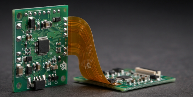
The flex zone now carries signals from side to side, as the spine bends to allow the book to open and close as it should. This is quite different from a simple flex PCB. A pure flex board bends in all directions, while a rigid flex circuit bends only when the designer specifies. That's the controlled combination that makes it popular for 3D packaging, in which the board needs to fold so it can fit in an enclosure. This yields a mechanically sturdy assembly, lighter weight, and a much greater tolerance to shock and vibration than a pile of individual boards connected through ribbon cables.
Rigid Flex Circuit Structure and Layer Stackup
Flex core is typically a layer of copper foil (one or two) over a polyimide film and is the heart of every rigid-flex board. The rigid regions are constructed around this core in a manner similar to that of a normal multilayer board by adding FR4 layers and prepreg on the outside. One concept is the use of a coverlay, a polyimide film that acts as a protective layer for the copper traces in the flex area rather than a liquid solder mask, as is done on the rigid portions. Coverlay is flexible and durable, and as a result has a much longer life for repeated bending than standard solder mask. A simplified example of a typical 4-layer rigid-flex stack-up is presented below:
| Layer | Region | Material | Typical Thickness |
| Top copper | Rigid only | Copper foil | 1 oz (35 µm) |
| Inner layer 1 | Flex + rigid | Rolled copper on polyimide | 0.5 oz (18 µm) |
| Inner layer 2 | Flex + rigid | Rolled copper on polyimide | 0.5 oz (18 µm) |
| Bottom copper | Rigid only | Copper foil | 1 oz (35 µm) |
The outer rigid layers terminate at the edge of the bend area, and the flexible layers extend throughout the entire board. The boundary between the rigid material and the flex is known as the transition region, and, as we will see later, it is the most sensitive to stress of any part of the board.
Materials Used in Rigid Flex Circuit Manufacturing
The material is the key to success or failure for a rigid-flex design. There's a job for each material, and if the wrong ones are mixed, then delamination or cracking is to be expected during thermal cycling. Let's delve into the key players.
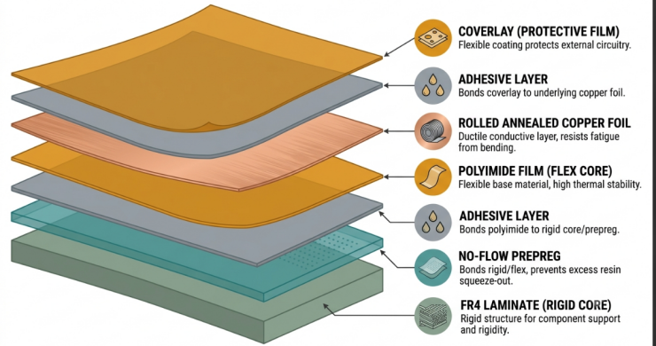
- Polyimide (PI) film: The backbone of the flex layer. It is thermally stable and will flex millions of times without fatigue at temperatures well above 200 °C. Some common brand examples include DuPont Kapton and Pyralux.
- Rolled annealed (RA) copper: This is used for flexible copper films on flexible boards and exhibits reduced creep properties. The copper of choice for dynamic flex zones is RA copper.
- Coverlay: A polyimide film with adhesive that seals and protects the flex traces to replace the solder mask in the bend area.
- FR4: The well-known glass-epoxy laminate that makes up the stiff part with the components.
- No flow prepreg: A special bonding layer with minimal resin flow during lamination to prevent resin from being squeezed into the flex area, causing stiffening. This is important in the transition from rigid to flex.
- Adhesives: The layers are bonded with acrylic or epoxy adhesives, although today, thinner and more reliable stackups are available without adhesive.
The thermal expansion coefficient (CTE) of these materials should be close to each other. A large mismatch between FR4 and polyimide results in internal stress each time the board is hot or cold, which causes long-term failure.
Common Types of Rigid Flex Circuits
All rigid flex circuit boards are not equal. These vary from a simple two-layer design to a complex 20+ layer design. These are the typical categories you will encounter:
- Single-sided flex with rigid ends: Conductive layer on one side of the flex, rigid at both ends. The easiest and least expensive choice.
- Double-sided rigid-flex: Two layers of copper with plated through holes. A good balance for most consumer products.
- Multilayer Rigid-Flex: Four layers or more, flex core typically carrying two layers and rigid areas as desired to 6, 8, or more. Widely used in high-density, high-performance electronics.
- Bookbinder (air-gap) construction: In multilayer dynamic flex, the layers of flex are not bonded in the flex, allowing each layer to move, thus significantly prolonging flex life.
Design Considerations for Reliable Rigid Flex Circuits
Key Benefits of Rigid Flex Circuits
It is best to first understand why the designers tolerate the added design effort. The reward is great:
- Fewer connectors and cables: Interconnects are in place, eliminating dozens of solder joints, which could fail.
- Space and weight saving: The board can be folded into 3D shapes, thus freeing up valuable volume in compact products.
- Improved reliability: where fewer joints are used and vibrations are more of an issue, they are used, such as in the aerospace and medical fields to increase service life.
- Simplified assembly: One integrated part equal to several boards and their wiring harnesses.
- Improved signal integrity: Eliminates connector transitions and decreases impedance discontinuities on critical signals.
To sum up the flex pcb vs rigid flex pcb comparison, a pure flex board works well for a straightforward bendable interconnect, while a rigid-flex board offers built-in flexibility and the stability to mount components.
Bend Radius and Stackup Design
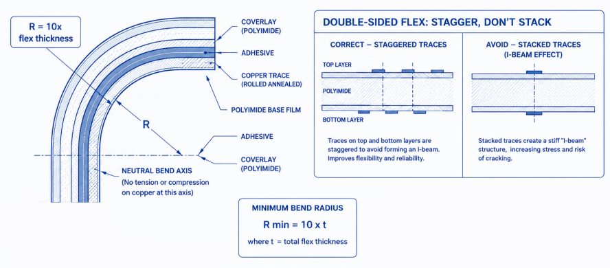
The most critical number in your design is the “bend radius”, or the tightest radius to which the flex section can be bent. It will stretch the copper on the outside too far if you bend it too sharply, and it will crack. The safe minimum will vary based on the number of layers and the type of flex (static or dynamic). A general guideline is to use the minimum bend radius in relation to the overall flex thickness:
| Flex Type | Layers | Minimum Bend Radius |
| Static (bend to install) | Single-sided | 6× flex thickness |
| Static | Double-sided | 10× flex thickness |
| Static | Multilayer | 12–20× flex thickness |
| Dynamic (repeated flexing) | Any | 100× flex thickness |
People speak of the 10× thickness rule, but it is really a lower bound, and if the application is dynamic (such as a print head or a folding hinge), many products can achieve millions of cycles at 10×, 20×, or more. The other half of the equation is to keep the copper on the neutral bend axis, where stretching and compression are balanced. See Sectional Design Standard IPC-2223 for the detailed bend and stackup requirements. The "bible" of design for all things flex.
Component Placement and Routing
Bend radius is not the only critical factor; where parts go and where traces are routed in the flex is also significant. Golden rule: avoid components and vias in flex/transition areas. These areas are in motion, and hard elements in these areas become stress concentrations and cracks. These are the routing practices to use in and around the flex zone:
- Route runs across the bend line, stretching the length of the copper, not the width.
- Avoid right angles; use curves instead.
- With double-sided flex, stagger the traces on the two sides of the board rather than stacking them directly on top of each other. Stacked copper creates both a stiff "I-beam" and a structure that is resistant to bending and cracking.
- Use teardrops at pad-to-trace connections to distribute mechanical stress.
- Plated through-hole features should be at least 50 mils away from the rigid-to-flex transition.
- Do not use solid pours on the flex; instead, use hatched or cross-hatched copper pours to keep the flex flexible.
Signal Integrity and Reliability Considerations
Rigid-flex is not just a mechanical issue...high-speed signals need to make it through the flex. Because polyimide has a lower dielectric constant (3.2-3.5) than FR4 (4.3), a controlled-impedance trace width changes when it moves from a rigid to a flex board. You need to consider both dielectrics in your stackup calculations. For differential pairs and controlled-impedance lines, provide a continuous reference plane under the signals as much as possible. Solid ground planes are inflexible in the flex; many of the designers employ cross-hatching ground planes as an intermediate solution between shielding and flexibility. Here is some reliability information to watch:
- Match the CTE of the adjacent materials to minimize the thermal-cycling stress.
- Prevent discontinuities in impedance at the transition region where both the dielectrics and geometry change.
- Include strain relief at the transition to prevent the concentration of the bending stress on the copper.
Typical Applications of Rigid Flex Circuits
Medical and Wearable Electronics
Medical and wearable devices are a logical fit. Dense electronics in curved body-worn enclosures are required for hearing aids, pacemakers, insulin pumps, continuous glucose monitors, and others. A rigid-flex board folds up to fit into the housing and maintains the sensitive circuitry rock solid. There's no margin for error here: An implantable device cannot have a loose connection. Rigid-flex eliminates those weak points by incorporating the intercon into the board. Smartwatches and fitness bands are other types of wearables that take a similar approach to putting a battery, display, and sensor board around a small volume.
Automotive Electronics
Cars are tough; they vibrate, they experience extremes of temperature, and they are expected to last for decades. Rigid flex circuit boards excel in engine control units, ADAS camera modules, dashboard displays,s and EV battery management systems. The most important selling point is the vibration tolerance. A traditional board-plus-connector assembly can wear loose over years of driving, whereas there are few joints that can fatigue in an integrated rigid-flex. This is the reason that more and more carmakers are turning to rigid-flex construction, which is designed to IPC Class 3 reliability for safety-critical systems.
Consumer Electronics and Compact Devices
This is the volume market. Rigid-flex is essential in smartphones, tablets, laptops, digital cameras, drones, and foldable devices, among other applications, to achieve thin, light form factors. The flex part of the board will bend tens of thousands of times in a folding phone, which is a classic dynamic flex application. Rigid-flex is used for camera modules for the image sensor board to be bent back against the main board to save precious millimeters. Rigid flex circuit boards are no longer a luxury, but rather a requirement with the continued miniaturization of devices.
Rigid Flex Circuit Manufacturing Process
Design Review and DFM Optimization
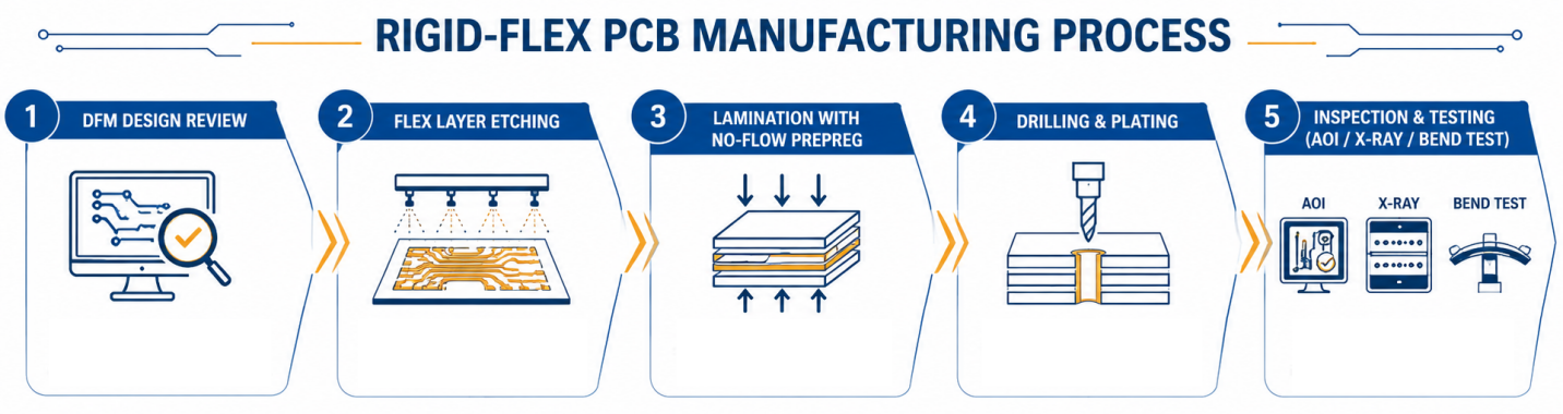
It all begins with a good Design for Manufacturability (DFM) review. Rigid-flex combines flexible and rigid materials, so minute design details such as bend radius, transition placement, and coverlay openings yield disproportionate results in terms of yield and cost. A good manufacturer will review your stack-up, make sure that vias and components do not fall into the flex zone, and ensure you are using a bend radius compliant with IPC-2223. Modern fabricators such as JLCPCB will provide engineering DFM feedback prior to production, which will identify problems at an affordable rate and not an expensive rate on the production floor.
Flexible Layer Fabrication and Etching Process
Then, the flex core is created. The base flex laminate is made of a thin, rolled copper sheet laminated to polyimide film. This is the layer that will conduct signals around the bend, and the quality of the material used will be directly proportional to the flex life. Then the circuit pattern is made by photolithography:
- Spin the photoresist on top of the copper.
- Expose using a photomask that contains the trace pattern.
- Remove unexposed resist with a solvent.
- Remove the copper from the unwanted areas, leaving the traces.
- Remove the rest of the resist.
Once the etching is complete, the coverlay is laminated on top of the etched flex traces to protect and insulate the flex traces. Coverlay has openings cut where pads or vias are required to be connected.
Lamination and Bonding Process
The resulting combination of rigid and flex layers is a single stack. In a lamination press, the FR4 layers, prepreg, and flex core are stacked with precision, and heat and pressure are applied to bond the layers together. This is where no-flow prepreg comes in handy. With the standard prepreg, the resin would squeeze out into the flex zone and harden it, destroying the flex. No-flow prepreg is formulated to remain in place, ensuring that the flex area remains clean and flexible all the way to the transition line. Once laminated, the board is then drilled, and the board's holes are plated in the same way as a rigid board is plated to join the layers. Lastly, the outline is routed, and the flex areas are released.
Quality Inspection and Testing
Since there are more potential failure modes compared to a standard board, rigid-flex requires more inspection. Manufacturers usually conduct a multi-stage inspection system:
- Automated Optical Inspection (AOI) to detect etching faults and trace faults.
- Inspection with X-ray to ensure plating and inner-layer registration.
- Open and short electrical test (flying probe or bed of nails).
- Bend/flex test dynamic designs to ensure the board will survive the number of cycles it is rated for.
- Controlled impedance builds impedance testing.
Certification matters too. Find fabricators that conduct inspections to IPC-A-600 (board acceptability) and are fabricating to IPC-6013, the performance spec for flexible and rigid-flex printed boards. IPC Class 2 is used for the majority of commercial applications, and Class 3 is intended for high-reliability medical and aerospace applications.
Conclusion
A rigid flex circuit offers the benefits of both rigid FR4 for mounting components and polyimide flex for routing signals. That combination makes it the foundation of compact, reliable electronics in medical, automotive, and consumer products alike. The “take-home messages” are easy to remember but can be overlooked. Don't ignore the bend radius, avoid having components or vias in the flex or transition areas, don't neglect CTE matching, and get your manufacturer involved early with a real DFM review.
Nail those, and you have a board that's often more dependable than the rigid-plus-cable assembly it takes the place of. The trend of miniaturization will continue to increase as the need for reliability continues to go up and up, making rigid-flex more and more integral to today's design. When you're ready to go from concept to a working prototype, you can easily build a well-made board in no time at all with JLCPCB's rigid-flex fabrication and upfront DFM support.

Frequently Asked Questions (FAQ)
Q: What is the difference between a flex PCB and a rigid-flex PCB?
Ans: A flex PCB bends across its entire body and is used purely as a flexible interconnect, while a rigid-flex PCB combines stiff FR4 regions for mounting components with flexible polyimide regions for routing. Rigid-flex gives you component stability and controlled bending in one integrated board.
Q: What is the minimum bend radius for a rigid flex circuit?
Ans: For static (bend-to-install) designs, plan on roughly 6× the flex thickness for single-sided, 10× for double-sided, and 12–20× for multilayer. Dynamic designs that flex repeatedly should use about 100× the thickness to reach millions of cycles, per IPC-2223 guidance.
Q: Which materials are used in rigid flex circuit boards?
Ans: The flex layers use polyimide film with rolled annealed copper and a coverlay for protection, while the rigid sections use FR4. No-flow prepreg bonds the two systems together without letting the resin stiffen the flex area.
Q: Why are rigid flex circuits more expensive than rigid PCBs?
Ans: They require more materials, more process steps like separate flex fabrication and precise lamination, and more inspection, such as X-ray and bend testing. However, the total system cost often drops because you eliminate connectors, cables, and assembly labor.

Popular Articles
• Choosing the Right Bend Radius for Durable Flexible PCBs
• Flexible Meets Durable: Understanding Rigid-Flex PCB Technology
• PCB Stiffeners: An Essential Requirement for Flexible Circuits
• The Ultimate Guide to Flexible PCB: Types, Design, and Applications
• 45 Must-Know Flex PCB Design Tips You Can't Afford to Miss!
Keep Learning
Choosing the Right Bend Radius for Durable Flexible PCBs
Key Takeaways Mastering the bend radius is essential for reliable flexible PCB design. Following IPC-2223 guidelines, maintain a minimum of 6× total thickness for static bends and 100× for dynamic applications, while using thinner RA copper, adhesiveless polyimide, staggered traces, and cross-hatched patterns in flex zones. Proper material selection, layer stackup optimization, and adequate clearance from stiffeners can dramatically extend flex life and prevent premature trace cracking or delamination......
Flex PCB Stackup Design Guide: Layers, Materials & Reliability
Key Takeaways A reliable flex PCB starts with the right stackup design. The layer structure, material selection, and copper arrangement directly affect flexibility, bend life, electrical performance, and manufacturing reliability. This guide explains single-sided, double-sided, and multilayer flex PCB stackups, including polyimide materials, coverlay, copper types, and key design considerations for creating durable flexible circuits with JLCPCB. Did you ever wonder how a foldable phone can last for 20......
Flexible Meets Durable: Understanding Rigid-Flex PCB Technology
In the rapidly evolving world of electronics, the demand for smaller, more reliable, and more versatile devices continues to grow. To meet these demands, engineers and designers are increasingly turning to Rigid-Flex PCBs. The circuit boards combine rigid and flexible substrates into a single interconnected structure. This combination allows for complex designs that can bend and flex in specific areas while maintaining rigidity in others. To manufacture rigid flex PCBs, IPC offers advice and best prac......
PCB Stiffeners: An Essential Requirement for Flexible Circuits
A printed circuit board stiffener plays an important role when it comes to offering mechanical support to a PCB. They are particularly helpful for flexible circuit boards, that given their name, are flexible and in need of stiffness in certain places. Stiffeners are particularly required when components are placed in a flex zone & the weight of these components stresses the flex material. These components provide a rigid connection from the flexible portion to the solid board. This solidity makes appl......
The Ultimate Guide to Flexible PCB: Types, Design, and Applications
Key Takeaways JLCPCB 1–4 Layer Flex PCB: Supports 1 to 4-layer FPCs with polyimide (PI) substrates and trace/space down to 3/3 mil. Stiffener Selection: Use PI (0.1–0.25mm) for ZIF connectors, FR4 (0.1–1.6mm) for SMT support, and Stainless Steel (0.1–0.3mm) for high rigidity. Layout Optimization: Use cross-hatched copper ground planes and stagger 2-layer traces to eliminate the "I-Beam effect." Surface & Protection: Combine Immersion Gold (ENIG 1u"/2u") for SMT planarity with flex coverlay to protect ......
Medical Flex Circuits: Manufacturing, Applications, Materials, and Design Guide
Medical flex circuits made to fit inside a 1.0 mm disposable endoscope, wrap around a hearing aid shell, and sit on a patient's arm for ten straight days. When one fails, it is not a warranty return but a device history file and a regulatory conversation. In this guide, you will learn: What separates a medical flex circuit from a consumer one How they are built, tested, and released Polyimide, copper, coverlay, and stiffener choices Fine line, bend radius, and layer count limits What to check before c......