Double-Sided FPC: Structure, Stack-Up, Benefits, and Manufacturing Guide
17 min
- What Is a Double-Sided FPC?
- Double-Sided FPC Structure and Stack-Up Design
- Benefits and Applications of Double-Sided FPC
- Design Considerations for Double-Sided FPC
- Double-Sided FPC Manufacturing Process
- Common Challenges in Double-Sided FPC Design and Manufacturing
- Why Choose JLCPCB for Double-Sided FPC Manufacturing
- Conclusion
- FAQ
Have you ever unzipped a folding phone, a camera module, or a wearable and tried to figure out how all these signals fit within a ribbon as thin as a credit card? It is nearly always a double-sided FPC, which is a flexible printed circuit having copper on both sides of a polyimide film. It is flexible, it can be folded, and it still fits routing that is heavy and fast, which would be difficult to get on a rigid board.
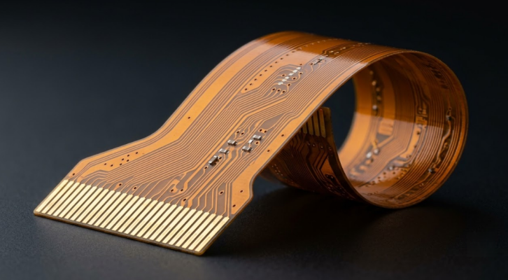
Single-sided flex is ideal for easy routing. However, once you start getting more signal counts, you're in a hurry to move. This is where routing over two layers of copper, with plated through holes, makes all the difference. Almost doubling the number of wires you can fit on the same footprint. In this guide, we'll explore what exactly a “double-sided FPC” is, how it is constructed from layer to layer, why engineers choose to use it, and how it's manufactured. We'll leave the numbers intact: copper weight, polyimide thickness, and bend radius rules, so you can feel confident using this in your next design.
What Is a Double-Sided FPC?
Definition and Basic Structure
A double-sided flex circuit is a flexible circuit with conductive copper patterns on both sides of a single flexible dielectric core. The core is almost always polyimide (PI) film and is highly valued for its high thermal stability and high mechanical strength. Plated-through-holes (PTH) are used to electrically connect two copper layers wherever it is desired. So that signals can jump from the top layer of the board to the bottom layer. It's like a two-lane road that fits back-to-back on a thin, flexible spine. A double-sided FPC will provide you with 2 lanes of copper.
This is obtained by having 2 layers of copper with vertical elevators (vias) drilled and plated through the film. It is similar to the operation of a rigid double-sided printed circuit board, except that there are two copper layers, holes plated through the layers, and a coverlay or soldermask on the top layer. The dielectric material is a thin film of PI, typically 12.5 µm, 25µm, or 50 µm, which allows the completed circuit to flex, fold, and route around very tight mechanical corners.
Double-Sided FPC vs. Single-Sided FPC
The best way to understand a double-sided FPC is to compare it with a single-sided FPC. If the flex is only on one side, then all the flex traces must share the same side. Cross one signal over another, and you're forced to add on a jumper or a cumbersome detour.
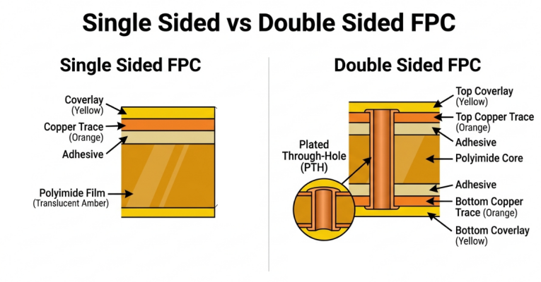
On the other hand, two copper layers for routing on the front, routing on the back, and crossing signals with vias freely. If you design a double-sided layout as opposed to a single-sided layout, and use the same design rules, you will find that you can reduce the size of your board by about 50% just because you have the wiring real estate on both sides.
| Feature | Single-Sided FPC | Double-Sided FPC |
| Copper layers | 1 | 2 (top and bottom) |
| Layer interconnect | None (jumpers only) | Plated through holes |
| Wiring density | Lower | Up to ~2x higher |
| Crossover routing | Difficult | Easy via the back side |
| Flexibility | Highest | Slightly reduced |
| Typical cost | Lowest | Moderate |
Double-Sided FPC Structure and Stack-Up Design
Copper Layers, Polyimide Substrate, and Coverlay Structure
The double-sided FPC is a sandwich, and the knowledge of each slice helps to predict the thickness, flexibility, and impedance of the double-sided FPC. The polyimide core is located in the middle. A protective coverlay is placed over both sides, then a pattern is printed on the copper foil, and finally, a pattern is printed over the copper foil to form your circuit. Typical build (from top to bottom):
- Top coverlay: PI film (25 µm or 50 µm) + adhesive (12.5 µm or 25 µm) covering the top copper.
- The top copper foil is either rolled annealed (RA) or electro-deposited (ED), usually 18 µm (½ oz) or 35 µm (1 oz) thick.
- Flexible dielectric (usually 25 µm): the flexible material used for the core, which can be bonded with adhesives or without adhesive bonding.
- Bottom copper foil: The same weight as the top layer.
- The bottom coverlay: PI film plus adhesive, like the top.
The difference between RA and ED is more significant for copper foil than it appears. The rolled annealed copper grid features an elongated grain structure and will not break when bending over and over many times, hence the preferred use for dynamic-flex. For static installations, where the flex is bent just once and then kept bent, copper ED is suitable.
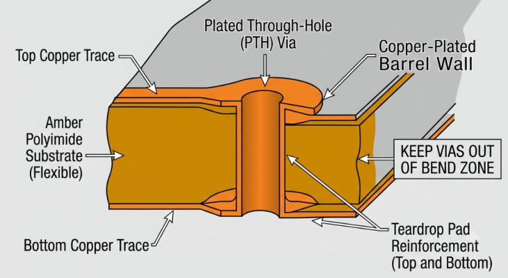
Via and Through-Hole Connections
The two-layer circuit is made up of the vias on a double-sided FPC. These are nearly always plated in flex by holes, a hole being drilled all the way through the polyimide and copper, the cross section then electroless and electrolytically plated with copper to form a conductive barrel. The double-sided flex land is typically made with minimum finished hole sizes of 0.20-0.30 mm, and a common, comfortable size is 0.25 mm. Advanced processes are able to reduce trace/space down to 0.06 mm/0.06 mm, but for most designs, 0.10 mm/0.10 mm is a safer and more profitable goal.
Plated barrel reliability depends on the location of the vias, not just routing decisions, due to flexing stresses on the substrate. Here are some "rules of thumb":
- Do not put vias in the bend area because it is a rigid or static area.
- Use teardrops at the point of intersection with the pad to minimize stress concentration.
- Do not use via-in-pad on flex unless it is filled and planarized.
If you get the vias right, you have a reliable, flexible double-sided PC board; if you get the vias wrong, it will be the first thing to fail under flexing fatigue.
Benefits and Applications of Double-Sided FPC
Higher Wiring Density and Space Optimization
The biggest advantage is density. You fit much more signal into the same outline, routing on both faces, and gluing them together with vias. The figure of 50% versus 50% flex when compared to the single-sided is not a marketing figure: it's actually 50% versus 100%, which is the most important in products where every cubic millimeter is at stake. The ability to pack the interconnect tightly is the key to foldable phones, small camera modules, and hearing aids.
Improved Electrical Performance and Signal Integrity
Two layers of copper open up whole new avenues beyond density. One layer can be used as a ground/reference plane, and then signals can be routed against it, providing you with controlled impedance, which is essential for high-speed differential pairs such as USB, MIPI, and LVDS. Crosstalk and electromagnetic interference are also controlled by providing a clean short return path under each signal in a continuous reference plane. Rudimentary on one-sided flex, disciplined on a double-sided flex. It's not a feature added for your convenience, but a signal integrity upgrade.
Consumer Electronics, Automotive, and Medical Applications
Double-sided flex circuits are found practically anywhere modern electronics can fold or fit, due to their density, flexibility, and reliability. Some typical places in which they live:
- Consumer electronics: smartphone hinges, laptop screens, camera components, and wearable electronics.
- Consumer Electronics: Smart home systems, LED displays, and ADAS sensors.Industrial Electronics: Battery Management Interconnects, instrument clusters, and LED displays.
- Medical: Endoscopes, hearing aids, patient monitors, and sensor leads for implants.
- Industrial: Robotics joints, machine vision heads, factory automation sensors.
In each of these, a rigid double-sided PC board would not fit mechanically, and a single-sided flex board would not accommodate the number of signals. The target is the sweet spot on the double-sided flex.
Design Considerations for Double-Sided FPC
Layer Stack-Up and Material Selection
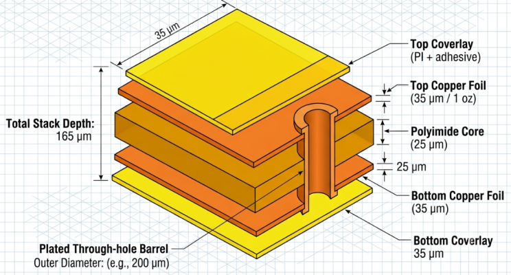
The key to good flex design is designing the stack-up first, before laying out a single trace! Polyimide thickness (12.5, 25, or 50 µm) would be selected depending on the flexibility required and the mechanical load required. The thinner the polyimide, the more flexible it is, but it would not handle mechanical load as well. Combine with appropriate copper. In dynamic bend areas, use 18 micron/½ oz copper, but in power distribution areas, use heavier 35 micron/1 oz copper for heavier currents. In the case of a design that gets hot during operation, or one that requires the thinnest possible profile, we request that you use adhesiveless laminate, which will remove one entire adhesive layer from the stack.
Bend Radius and Flexibility Requirements
The number that distinguishes a flex circuit that will last millions of cycles from one that will crack in weeks is the bend radius. The basic rule is that the harder you bend, the more stress you incur on the outer copper layer. If the FPC is double-sided, a safe minimum bend radius is about 6 to 10 times the overall thickness of the circuit. A double-sided stack will have a larger absolute bend radius than a single-sided one.
| Flex Type | Recommended Minimum Bend Radius |
| Single-sided FPC | 3–6× thickness |
| Double-sided FPC | 6–10× thickness |
| Multilayer flex | 10–20× thickness |
If an application is one that flexes continuously, always design it with the high end of that range in mind, and for such applications, always orient traces across the bend axis to distribute the flex.
Via Design and Trace Routing Optimization
There is a grammar for routing on Flex. Continue these practices, and your yield and reliability improve:
- Don't align vias across a bend (they will form a tear line).
- Avoid sharp corners (90°), use curves to spread out mechanical stress.
- Use teardrops wherever there is a junction between pads and a trace to strengthen the transition. Carefully cross-reference planes; do not use high-speed signal planes over splits or gaps in the ground plane.
- Wherever there is an issue of impedance control or EMI, use a solid ground layer on one side.
Mechanical requirements and how well the board performs electrically are closely tied to a flexing substrate, and the small routing decisions determine the board's survival during its service life.
Double-Sided FPC Manufacturing Process
Circuit Pattern Formation and Precision Etching
The manufacturing process starts with a copper-clad polyimide laminate with a double-sided coating. The first step is to transfer your circuit to both faces of copper. The photoresist is laminated over the copper, exposed to the photoresist through a photo-tool containing your artwork, and developed to leave only photoresist over the copper areas where you want.
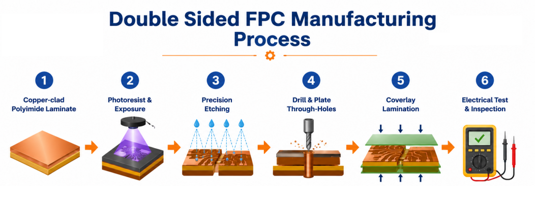
Then there is precision etching, in which a chemical etchant will eat away all copper that is not "protected" by your traces. For thin lines (less than 0.06 mm) on double-sided flexible circuits, etch control is key; over-etching will make lines narrow, and under-etching will cause shorts. Following resist removal, both circuit layers remain, but are not yet connected. The holes are drilled through the laminate and then metalized (electroless copper seed layer to coat the walls of the holes, and then electrolytic copper plating to form the plated through holes between top and bottom).
Lamination and Coverlay Processing
With the circuit patterned and the vias plated, the flex needs protection. Flex is usually coated with a coverlay, a pre-cut piece of polyimide film with adhesive that is laid over the copper and heat and pressure cured. Liquid solder mask is not used with flex, as it can be damaged. Coverlays for pads and connector fingers are typically cut out prior to lamination, via drilling, punching, or laser. Registration here is very demanding, as if a coverlay is misaligned, it can reveal copper that should be in the coverlay, or it can cover a pad that needs to be open. Where finer openings are needed, a 10-15 µm liquid photoimageable (LPI) coverlay is used for some designs.
Electrical Testing and Reliability Inspection
No flex ships until verified. Each panel is subjected to an electrical test (flying-probe or bed-of-nails) to ensure continuity for each net and also to ensure that there is no contact between an isolation and a net where there should not be. This catch opens up from etch defects and process residue shorts. In addition to electrical testing, Flex's trust is gained through reliability inspection. Common steps include:
- Automated Optical inspection (AOI) of trace width, spacing, and defects.
- Cross-section to check the vias plated thickness.
- Dynamic flex testing – repeated bend cycles and c
- heck for bend zone endurance.
- Thermal shock and solderability tests to ensure the stack is able to withstand assembly reflow.
This is the stage that can be followed by surface finishes like ENIG (electroless nickel immersion gold) and HASL, applied before or during this process, to prevent any exposed copper and ensure solderability during assembly.
Common Challenges in Double-Sided FPC Design and Manufacturing
Mechanical Stress Management
Fatigue is the number one problem that makes flex unique. Each bend cycle will cause stress to the copper, and the copper that is on the outside of a bend will extend, while the copper that is on the inside will compress. In thousands or millions of cycles, if the stress used is not managed properly, it could cause cracks in the traces or may fracture the via barrels. Discipline is the answer: Do not put vias in bends, use RA copper in dynamic areas, bend traces, and follow the 6× to 10× bend radius rule. Additionally, a lot of behind-the-scenes work is done by stiffeners and strain-relief features at transitions between areas that flex and areas that are stiff.
Signal Integrity and Manufacturing Yield
Whereas with the electrical side, thin dielectrics present problems for impedance control. The 25 µm thick polyimide core is much thinner than a rigid FR4 dielectric, so trace width tolerances have a disproportionately large influence on the impedance. A small etch variation can cause your 90 Ω differential pair to come out of spec. The other pressure point is yield. The difficulty goes up with fine 0.06 mm traces, tight coverlay registration, and plated barrels on a moving substrate. That's why it's wise to select a manufacturer that has a well-developed FPC line and has automated the design-rule checking process. The margin they have built into the process makes the difference between a good idea and a reliable, repeatable double-sided printed circuit board (PCB) product.
Why Choose JLCPCB for Double-Sided FPC Manufacturing
Advanced FPC Fabrication Capabilities
The process line is optimized for polyimide, not rigid FR4, and is required to build a good double-sided flex. JLCPCB is a modern manufacturer that has a dedicated FPC fabrication system to offer a wide variety of surface finishes (ENIG, immersion, etc.) and plated through-holes that a dense double-sided flex can use. This capability breadth allows you to use RA copper for dynamic bends, adhesiveless laminate for thin thermal critical stacks, or controlled impedance when it's required for high-speed signals.
Automated DFM Review
With Flex, it's important to get them right before they even reach the fabrication line. An automated DFM (Design for Manufacturability) review identifies issues such as vias in bend areas, traces too near to coverlay openings, spacing that is too close to the process limit, and more, before your board even reaches the line. This first pass is automated, coupled with real capability data, and is what you don't want to experience: the classic flex failures that only appear after assembly. For those who wish to implement these principles, JLCPCB's instant quoting and DFM checks enable you to validate the double-sided flex design early on, making the process uncomplicated.
Rapid Prototyping and Volume Production Support
Development of the flex is an iterative process; you want to bend-test the prototype before making decisions about volume. With a fast turnaround, it shortens that loop and allows you to test out the bend radius and get hardware in place within days or weeks. This same line then scales to volume once your design is finalized, ensuring that you don't re-qualify a new supplier between prototype and production. That continuity and the flex price competition are what make a manufacturer a true partner and not simply a vendor for a double-sided flex program.
Conclusion
Flexible circuits are grown on a double-sided FPC. Plated through the holes joins them to double the routing density, allows for true controlled-impedance signaling, and retains the flexibility of a fold-anywhere board. The fine print is the art, using copper for the bends, avoiding placing vias in the bend region, a 6–10× bend radius, and a close registration of coverlay placement.
Get them right, and you've got an interconnect that lasts for millions of flex cycles in phones, cars, and medical devices. Double-sided flex will continue to play an even greater role in product design in the future, as electronics shrink and fold. When you are ready to switch from schematic to a real, bendable board, you'll find it much safer when you work with a manufacturer that has an established FPC line and automated DFM, such as JLCPCB.

FAQ
Q: What is a double-sided FPC?
Ans: A double-sided FPC is a flexible printed circuit with copper conductor patterns on both sides of a polyimide film core, connected by plated through holes. This dual-layer structure roughly doubles the wiring density compared to single-sided flex while keeping the circuit bendable.
Q: How is a double-sided FPC different from a rigid double-sided printed circuit board?
Ans: Both have two copper layers joined by plated through holes, so the electrical principle is identical. The difference is the substrate — a flex circuit uses thin polyimide film so it can bend and fold, while a rigid board uses stiff FR4 that cannot flex.
Q: What is the minimum bend radius for a double-sided flex circuit?
Ans: A safe minimum bend radius for a double-sided FPC is about 6 to 10 times the total circuit thickness. For dynamic applications with continuous flexing, design toward the higher end of that range to maximize fatigue life.
Q: What copper weights are used in double-sided FPC?
Ans: Common copper weights are 18 µm (½ oz) and 35 µm (1 oz), with lighter 12 µm and heavier 70 µm options available. Rolled annealed (RA) copper is preferred for bending zones because its grain structure resists cracking far better than electro-deposited copper.
Q: Can double-sided FPC support controlled impedance and high-speed signals?
Ans: Yes. Using one copper layer as a continuous ground reference lets you route controlled-impedance signals on the other, which is essential for high-speed interfaces like USB, MIPI, and LVDS. The reference plane also reduces crosstalk and EMI.
Q: Why do vias need to stay out of the bend area on a double-sided FPC?
Ans: Plated through holes are rigid points in an otherwise flexible circuit, so bending them concentrates mechanical stress on the barrel and can crack it. Keeping vias in the rigid or static zones and staggering them greatly improves flex-fatigue reliability.

Popular Articles
• Choosing the Right Bend Radius for Durable Flexible PCBs
• Flexible Meets Durable: Understanding Rigid-Flex PCB Technology
• PCB Stiffeners: An Essential Requirement for Flexible Circuits
• The Ultimate Guide to Flexible PCB: Types, Design, and Applications
• 45 Must-Know Flex PCB Design Tips You Can't Afford to Miss!
Keep Learning
Choosing the Right Bend Radius for Durable Flexible PCBs
Key Takeaways Mastering the bend radius is essential for reliable flexible PCB design. Following IPC-2223 guidelines, maintain a minimum of 6× total thickness for static bends and 100× for dynamic applications, while using thinner RA copper, adhesiveless polyimide, staggered traces, and cross-hatched patterns in flex zones. Proper material selection, layer stackup optimization, and adequate clearance from stiffeners can dramatically extend flex life and prevent premature trace cracking or delamination......
Flex PCB Stackup Design Guide: Layers, Materials & Reliability
Key Takeaways A reliable flex PCB starts with the right stackup design. The layer structure, material selection, and copper arrangement directly affect flexibility, bend life, electrical performance, and manufacturing reliability. This guide explains single-sided, double-sided, and multilayer flex PCB stackups, including polyimide materials, coverlay, copper types, and key design considerations for creating durable flexible circuits with JLCPCB. Did you ever wonder how a foldable phone can last for 20......
Flexible Meets Durable: Understanding Rigid-Flex PCB Technology
In the rapidly evolving world of electronics, the demand for smaller, more reliable, and more versatile devices continues to grow. To meet these demands, engineers and designers are increasingly turning to Rigid-Flex PCBs. The circuit boards combine rigid and flexible substrates into a single interconnected structure. This combination allows for complex designs that can bend and flex in specific areas while maintaining rigidity in others. To manufacture rigid flex PCBs, IPC offers advice and best prac......
PCB Stiffeners: An Essential Requirement for Flexible Circuits
A printed circuit board stiffener plays an important role when it comes to offering mechanical support to a PCB. They are particularly helpful for flexible circuit boards, that given their name, are flexible and in need of stiffness in certain places. Stiffeners are particularly required when components are placed in a flex zone & the weight of these components stresses the flex material. These components provide a rigid connection from the flexible portion to the solid board. This solidity makes appl......
The Ultimate Guide to Flexible PCB: Types, Design, and Applications
Key Takeaways JLCPCB 1–4 Layer Flex PCB: Supports 1 to 4-layer FPCs with polyimide (PI) substrates and trace/space down to 3/3 mil. Stiffener Selection: Use PI (0.1–0.25mm) for ZIF connectors, FR4 (0.1–1.6mm) for SMT support, and Stainless Steel (0.1–0.3mm) for high rigidity. Layout Optimization: Use cross-hatched copper ground planes and stagger 2-layer traces to eliminate the "I-Beam effect." Surface & Protection: Combine Immersion Gold (ENIG 1u"/2u") for SMT planarity with flex coverlay to protect ......
Medical Flex Circuits: Manufacturing, Applications, Materials, and Design Guide
Medical flex circuits made to fit inside a 1.0 mm disposable endoscope, wrap around a hearing aid shell, and sit on a patient's arm for ten straight days. When one fails, it is not a warranty return but a device history file and a regulatory conversation. In this guide, you will learn: What separates a medical flex circuit from a consumer one How they are built, tested, and released Polyimide, copper, coverlay, and stiffener choices Fine line, bend radius, and layer count limits What to check before c......