How Flex Circuit Manufacturers Deliver Reliable Flexible PCB Solutions
14 min
- What Is a Flex Circuit Manufacturer and Why Does It Matter
- Flex Circuit Manufacturing Process and Key Production Steps
- Flex Circuit Design Guidelines for Reliable Manufacturing
- Flex Circuit Applications in Wearables and Compact Electronics
- Why JLCPCB Is a Trusted Flex Circuit Board Manufacturer
- Conclusion
- FAQ
Ever wonder how a smartwatch manages to fit a whole circuit in a rounded wrist band, or how a folding phone can endure 200,000 hinge cycles? The solution almost always turns out to be the flexible printed circuit and the skill of the flex circuit manufacturer that creates it. These thin and flexible boards fit reliable electronics into places where a rigid FR4 board would not fit. However, constructing them reliably is a whole other ballgame than creating the normal stiff PCBs.
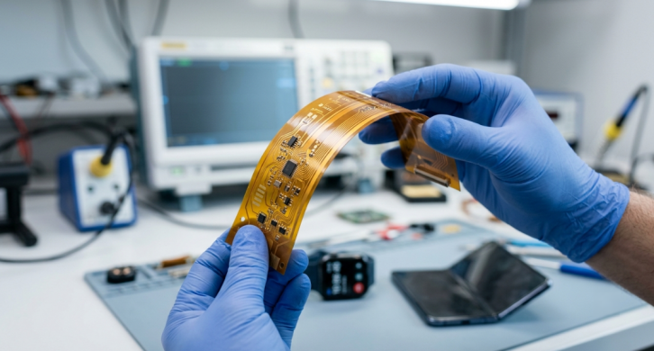
Flex circuits appear to be very simple. Just add a sheet of polyimide, a bit of copper traces, a coverlay, and we're finished, right? Not quite. Once a board needs to be bent, flexed, or folded repeatedly, all the way from the copper grain structure to the bend radius to the lamination pressure becomes relevant. Let's take a tour and find out how flex circuit board manufacturers actually produce reliable products. We will explore all manufacturing steps as well as the design rules and mantras to keep flexible boards alive under mechanical stress, real-world applications, and what to look for when choosing a partner for your next flex project.
What Is a Flex Circuit Manufacturer and Why Does It Matter
Definition of Flex Circuit Manufacturing
Flex circuit manufacturing involves the formation of conductive copper patterns on a thin, flexible film made from polyimide. This board can bend, twist, or fold to fit into three-dimensional areas. Flex circuits differ from rigid boards, which are cut from a solid piece of board and remain flat, because they are designed to be flexible. That one requirement affects the way that the manufacturer chooses copper, how they apply the adhesives, and how they test the product.
A good flex circuit manufacturer does not sacrifice mechanical durability to make room for other attributes; it is a part of the design. The main column is elegantly thin. A typical single-layer flex consists of a polyimide base film ranging from 0.5 mil to 5 mil (12.5 microns to 127 microns), a copper conductor layer, and a polyimide coverlay to protect the traces. All is in millimeter fractions.
Flex PCB vs Rigid PCB Manufacturing Differences
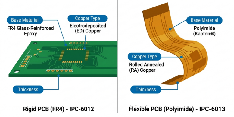
The distinctions between flex and rigid go beyond the substrate. Below is a comparison of the important parameters that differentiate the two processes.
| Parameter | Rigid PCB (FR4) | Flexible PCB (Polyimide) |
| Base material | Woven glass epoxy, around 1.6 mm typical | Polyimide film, 12.5 - 127 µm |
| Copper type | Electrodeposited (ED) | Rolled annealed (RA) for dynamic flex |
| Thickness | Rigid, fixed | Thin, bendable |
| Handling | Panel-based, robust | Requires careful handling, tension control |
| Protective layer | Solder mask (LPI) | Polyimide coverlay or flexible solder mask |
| Key standard | IPC-6012 | IPC-6013 |
The major difference practically is copper. For a rigid board, for instance, it's okay to have a vertical grain structure from an electrodeposited copper. Repeatedly flexed circuits employ rolled annealed copper that has a long horizontal grain structure, which resists cracking in response to repeated flex. One of the most obvious examples of a manufacturer who's familiar with dynamic flex is the switch of a single material.
Flex Circuit Manufacturing Process and Key Production Steps
Material Selection and Polyimide Substrate Preparation
It all begins with selecting the material. The manufacturer chooses a copper-clad polyimide laminate, choosing either adhesive or adhesiveless. Adhesiveless laminates have a lower thickness and are more thermally and dimensionally stable, which is important for fine pitch and high temperature work. The base film thickness is selected to meet the mechanical requirement.
Thinner (12.5 to 25 µm) polyimide bends more easily, and is appropriate for dynamic applications, while thicker film (50 to 127 µm) provides greater stability for static installations. The copper weight is also chosen at the same time, and is typically between 1/3 oz and 2 oz, with 1 oz (35 µm) being the standard. Chemical cleaning is done before any patterning occurs to remove oxides and contamination. Clean copper is very important since any residue will result in poor etch quality and poor adhesion downstream.
Circuit Patterning Through Photolithography and Etching
After the substrate has been prepared, the copper pattern is determined. This is where the circuit really comes to life.
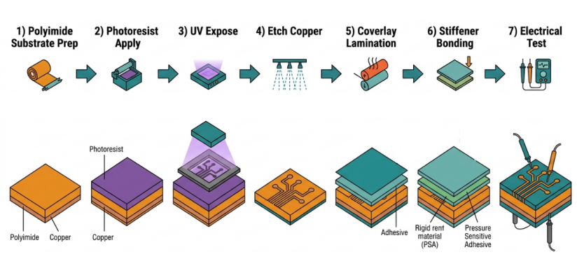
- Photoresist Application: This is a light-sensitive film that is applied to the copper surface.
- Expose: UV light is shone through a phototool or is laser imaged directly to harden the resist in the pattern of the traces.
- Develop: Remove unexposed resist, revealing the trace pattern.
- Etch: A chemical etchant is used to dissolve away the unwanted copper, leaving only the desired copper conductors.
- Strip: Any resist that remains is removed, leaving behind clean copper traces.
The minimum trace and space for fine-line flex work is approximately 3 mil / 3 mil (0.075 mm), and the minimum drilled hole is approximately 4 mil (0.1 mm). With high-density design requirements, laser drilling is able to process the smallest microvia. Yield and impedance accuracy are directly related to tight process control here.
Lamination, Coverlay, and Protective Layer Application
The copper pattern requires traces to be protected. Flex circuits can be covered with a coverlay, a laminated polyimide film with a pre-cut adhesive layer that covers the conductors. Coverlay open area is pre-cut to reveal pads and contact areas. The film is then placed on top of the circuit and laminated at heat and pressure to permanently adhere to the substrate.
The lamination pressure and temperature must be precisely controlled; otherwise, voids or trapped air cause delamination in the field. Manufacturers add stiffeners under connector areas and component pads made of polyimide, FR4, or aluminum for additional mechanical support in certain areas. This provides you with a flexible board, but still rigid landing zones wherever desirable. All completed panels are then electrically tested, typically 100 percent netlist verification per IPC-ET-652.
Flex Circuit Design Guidelines for Reliable Manufacturing
A good flex circuit is a joint responsibility between the flex circuit designer and manufacturer. No amount of good fabrication can help a design that doesn't respect the rules of mechanical physics in bending. The guidelines that keep flex boards alive are:
Minimum Bend Radius and Mechanical Flexibility Rules
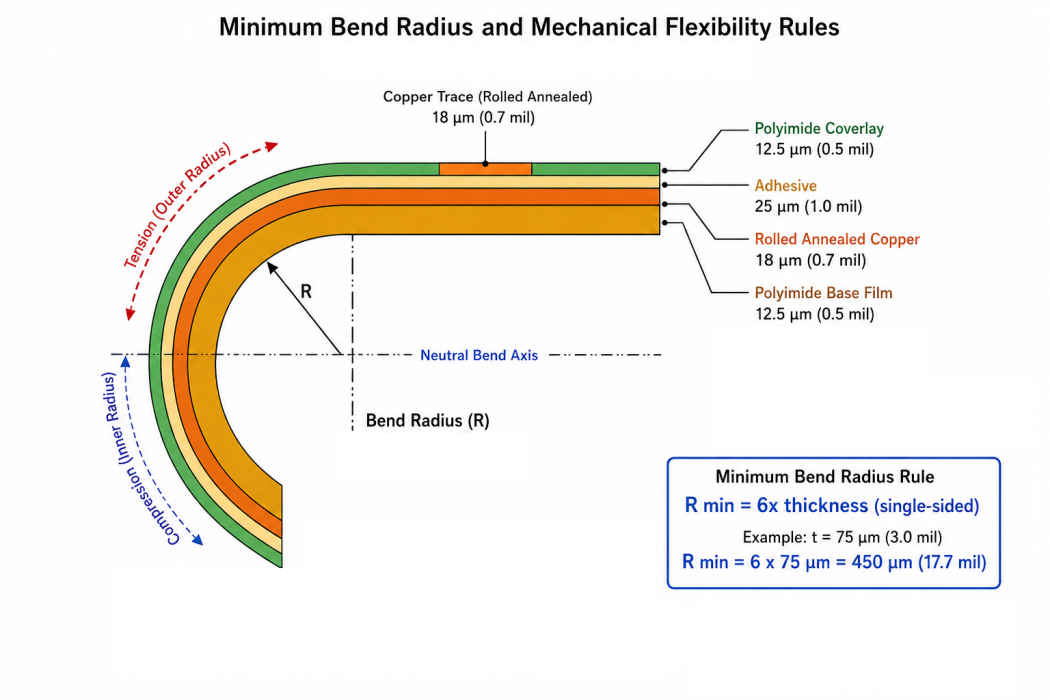
Bend radius is the most critical flex design rule. If bent too tightly, the outer copper will be stretched, causing it to crack. The safe minimum bend radius is dependent on the overall board thickness and the number of layers.
| Flex Type | Minimum Bend Radius (Static) | Dynamic Flex |
| Single-sided | 6× material thickness | Up to 20–40× |
| Double-sided | 10× material thickness | Higher, application-dependent |
| Multilayer | 15–20× material thickness | Generally avoided |
The static values will do if the board is only flexed once at installation, and then it remains stationary. However, for dynamic bending applications, with thousands or millions of flex cycles, a significantly greater radius and rolled annealed copper are desired, preferably with the flexing area limited to a single conductor layer. These decisions are made using IPC-2223 as a design framework.
Trace Routing and Copper Thickness Optimization
The routing of traces through the bend zone is a determining factor in reliability. There are some well-established guidelines.
- The route trace is perpendicular to the bend line, minimizing stretching of copper.
- Avoid sharp 90 degree corners as they focus stresses and use curved or teardrop traces.
- Use thin copper in flex areas, as thin copper (1/2 oz or thinner) will bend much more readily than heavy copper.
- The advantage of staggering the traces on double-sided flex is that the traces are not right on top of one another, making the bend stiffer and the neutral-axis stress higher.
- Use teardrops at pad-to-trace connections to minimize cracking at copper-to-via or pad connections.
There is a balance to the thickness of copper. The thicker the copper, the greater the capacity to carry more current and the more heat that it will generate, though it will be much less flexible. The sweet spot for most flex designs is 1/2 oz – 1 oz copper.
DFM Requirements for Manufacturability and Yield
This is where a good flex circuit board manufacturer comes in: DFM (Design for Manufacturability). These requirements help maintain high yields with low costs.
- Minimize trace and spaces (usually 3 mil / 3 mil for advanced flex).
- Ensure sufficient annular ring around vias for etching/drilling tolerances.
- Secure anchor pads with filleted transitions that won't peel when flexed and assembled.
- Under connectors and components, include stiffeners to avoid solder joint fatigue.
- Avoid having plated through holes in the bend area, as plated vias in a flex area are a common failure point.
Most of these issues are detected by a rapid DFM check prior to release. Most manufacturers, such as JLCPCB, have automated DFM checks that they perform on the files that are uploaded to them, and will alert you to any violations before the board ever reaches production.
Flex Circuit Applications in Wearables and Compact Electronics
Why Wearable Devices Require Flexible PCB Technology

Wearables are worn on moving and curvy surfaces. A fitness band, a smart ring, or a continuous glucose monitor must be worn around a wrist or finger and be comfortable and thin. Rigid boards just can't do this. In the case of a flex circuit manufacturer for wearables, the company is interested in ultra-thin stack, biocompatible material, and dynamic durability. The board might bend with each use of the user, meaning rolled annealed copper and a generous bend radius are common. Thin polyimide substrates also allow the device to be light enough to be worn throughout the day. Flex is also a reliability win because there are fewer connectors, and this product gets bumped, sweated on, and flexed a lot! The fewer the joints, the fewer the failure points in a harsh environment.
Reliability Requirements for Dynamic Bending Environments
The most severe reliability test for a flex board is dynamic bending. Millions of cycles flexing over the lifetime of a circuit magnifies the effects of small design or process defects into failures. There are several fronts on which manufacturers act to solve this problem.
- Crack-resistant rolled annealed copper.
- Very large bend radius, generally well above the static minimum, typically 100× or more for high-cycle applications.
- Single-layer flex zones to reduce stresses on stacked conductors.
- Coverlay and strain relief for smooth distribution of mechanical load.
This is supported by testing. Manufacturers verify design through flex cycle testing, thermal cycling, and 100% electrical verification. The performance classes are defined by IPC-6013, and class 3 is used for the highest reliability applications, such as medical and aerospace.
Why JLCPCB Is a Trusted Flex Circuit Board Manufacturer
Custom Flex and Rigid-Flex PCB Manufacturing Services
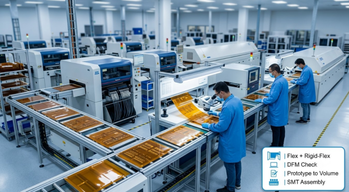
JLCPCB provides both pure flexible circuits and rigid-flex boards, which consist of rigid FR4 and flexible polyimide circuits in one board. Great for attaching heavy parts to a portion of your product that must bend down into a small area. JLCPCB is a rigid flex printed circuit board manufacturer that supports multilayer flex constructions, polyimide cover lay, ENIG surface finish, and stiffener options: polyimide, FR4, and aluminum. That includes anything from a single-layer interconnect to folding the assembly. The instant online quoting system also eliminates much friction. Upload your Gerber files, select your stackup and options, and receive a quote and DFM feedback in no time at all.
Advanced Engineering Support and DFM Optimization
The details of flex projects mean the difference between life and death, and this is where engineering support becomes important. Automated DFM analysis will verify that your design meets the manufacturing rules mentioned above and that bend radii are not too tight, vias are not in flex areas, and trace clearances are not too small before manufacturing begins. Early detection of these problems can save money and time. You find out about the problem at the design stage, rather than after you have built it, when you discover a crack in the trace. This type of pre-optimization is what sets a good flex circuit manufacturer apart from a board printer.
Scalable Production from Prototype to Mass Volume
The smooth road from prototype to volume is one of the greatest benefits a full-service partner brings. You can begin with a few prototype flex boards to prove your design, and then go on to hundreds or thousands of flex boards, all without changing vendors or re-qualifying your process. Combined with their SMT assembly service, your flex and rigid-flex boards will be populated and ready for testing. When you are taking flex circuit manufacturing from conception to a product ready for shipping, having prototyping, assembly, and volume manufacturing in the same location assures consistent quality and short lead times.
Conclusion
One of those technologies is flexible circuits. Whether it's the smartwatch on your wrist or the pacemaker keeping someone alive, a well-constructed flex circuit will get you there when a rigid board can't. That reliability comes through judicious material selection and process control, and through design rules that take into account the physics of bending copper. The bottom line is that making flex circuits is a partnership. The limits of reliability are dictated by your choices of bend radius, copper weight, and trace routing, and your manufacturer's process control is what determines if you achieve those limits.
If the two sides are right, flex circuits are more durable, lighter, and allow for greater packaging flexibility when compared to rigid boards. Wearables, medical devices, and IoT products are continuing to shrink in size, and this is just continuing to drive the demand for high-quality flexible and rigid-flex boards. Implementing these principles is easy if you're looking to go from prototype to production with DFM support along the way, which is what JLCPCB's flex and rigid-flex manufacturing services offer! Check out our layer stackups and materials guides for more information on layer stackups and materials, and check out our polyimide substrates and rigid-flex design guides.

FAQ
Q: What is the difference between a flex circuit and a rigid-flex circuit?
Ans: A flex circuit is built entirely on a flexible polyimide substrate and bends throughout. A rigid-flex board combines rigid FR4 sections with flexible polyimide interconnects in one assembly, letting you mount heavy components on the rigid areas while folding the flex sections into tight spaces.
Q: What is the minimum bend radius for a flexible PCB?
Ans: For static applications, the general rule is 6× material thickness for single-sided flex, 10× for double-sided, and 15–20× for multilayer. Dynamic bending applications require a much larger radius, often 20× to 100× or more, along with rolled annealed copper to resist cracking.
Q: Why do flex circuits use polyimide instead of FR4?
Ans: Polyimide is thin, flexible, and thermally stable up to well above 200°C, which lets the circuit bend without cracking. FR4 is a rigid glass-epoxy laminate that cannot flex, so it is unsuitable for any board that must bend, fold, or conform to a curved surface.
Q: What IPC standards apply to flex circuit manufacturing?
Ans: IPC-6013 covers the qualification and performance of flexible printed boards, and IPC-2223 is the sectional design standard for flex circuits. Electrical testing is often done to IPC-ET-652, and Class 3 designations under IPC-6013 apply to the highest-reliability medical and aerospace applications.
Q: Which copper type is best for dynamic flexing applications?
Ans: Rolled annealed (RA) copper is preferred for dynamic flex because its elongated horizontal grain structure resists cracking under repeated bending. Electrodeposited copper, common on rigid boards, has a vertical grain structure better suited to static or one-time flex installations.

Popular Articles
• Choosing the Right Bend Radius for Durable Flexible PCBs
• Flexible Meets Durable: Understanding Rigid-Flex PCB Technology
• PCB Stiffeners: An Essential Requirement for Flexible Circuits
• The Ultimate Guide to Flexible PCB: Types, Design, and Applications
• 45 Must-Know Flex PCB Design Tips You Can't Afford to Miss!
Keep Learning
Choosing the Right Bend Radius for Durable Flexible PCBs
Key Takeaways Mastering the bend radius is essential for reliable flexible PCB design. Following IPC-2223 guidelines, maintain a minimum of 6× total thickness for static bends and 100× for dynamic applications, while using thinner RA copper, adhesiveless polyimide, staggered traces, and cross-hatched patterns in flex zones. Proper material selection, layer stackup optimization, and adequate clearance from stiffeners can dramatically extend flex life and prevent premature trace cracking or delamination......
Flex PCB Stackup Design Guide: Layers, Materials & Reliability
Key Takeaways A reliable flex PCB starts with the right stackup design. The layer structure, material selection, and copper arrangement directly affect flexibility, bend life, electrical performance, and manufacturing reliability. This guide explains single-sided, double-sided, and multilayer flex PCB stackups, including polyimide materials, coverlay, copper types, and key design considerations for creating durable flexible circuits with JLCPCB. Did you ever wonder how a foldable phone can last for 20......
Flexible Meets Durable: Understanding Rigid-Flex PCB Technology
In the rapidly evolving world of electronics, the demand for smaller, more reliable, and more versatile devices continues to grow. To meet these demands, engineers and designers are increasingly turning to Rigid-Flex PCBs. The circuit boards combine rigid and flexible substrates into a single interconnected structure. This combination allows for complex designs that can bend and flex in specific areas while maintaining rigidity in others. To manufacture rigid flex PCBs, IPC offers advice and best prac......
PCB Stiffeners: An Essential Requirement for Flexible Circuits
A printed circuit board stiffener plays an important role when it comes to offering mechanical support to a PCB. They are particularly helpful for flexible circuit boards, that given their name, are flexible and in need of stiffness in certain places. Stiffeners are particularly required when components are placed in a flex zone & the weight of these components stresses the flex material. These components provide a rigid connection from the flexible portion to the solid board. This solidity makes appl......
The Ultimate Guide to Flexible PCB: Types, Design, and Applications
Key Takeaways JLCPCB 1–4 Layer Flex PCB: Supports 1 to 4-layer FPCs with polyimide (PI) substrates and trace/space down to 3/3 mil. Stiffener Selection: Use PI (0.1–0.25mm) for ZIF connectors, FR4 (0.1–1.6mm) for SMT support, and Stainless Steel (0.1–0.3mm) for high rigidity. Layout Optimization: Use cross-hatched copper ground planes and stagger 2-layer traces to eliminate the "I-Beam effect." Surface & Protection: Combine Immersion Gold (ENIG 1u"/2u") for SMT planarity with flex coverlay to protect ......
Medical Flex Circuits: Manufacturing, Applications, Materials, and Design Guide
Medical flex circuits made to fit inside a 1.0 mm disposable endoscope, wrap around a hearing aid shell, and sit on a patient's arm for ten straight days. When one fails, it is not a warranty return but a device history file and a regulatory conversation. In this guide, you will learn: What separates a medical flex circuit from a consumer one How they are built, tested, and released Polyimide, copper, coverlay, and stiffener choices Fine line, bend radius, and layer count limits What to check before c......