RGMII Routing Guidelines for Reliable Gigabit PCB Design
16 min
- Key Takeaways
- Introduction
- RGMII Specification Overview: Signals and Timing
- RGMII vs SGMII: Choosing the Right MAC-to-PHY Interface
- RGMII Routing Guidelines for PCB Design
- RGMII Layout Self-Check Checklist
- FAQs about RGMII Routing
- Conclusion about RGMII Routing
Key Takeaways
- RGMII is a 12-signal, single-ended, source-synchronous parallel interface; its TX and RX paths are separate timing groups.
- Match TXD[3:0] and TX_CTL to TXC. Match RXD[3:0] and RX_CTL to RXC. Do not match TX against RX.
- Budget the aggregate clock-to-data skew separately in each direction, and avoid unintentionally stacking a full PCB delay with an enabled silicon delay.
- Treat 50 Ω ±10%, 20 mil matching and a 6 inch route limit as TI layout guidance, not universal clauses of the RGMII specification.
- Minimize vias, preserve the reference plane and select any series termination from the real driver impedance and signal-integrity model.
Introduction
A Gigabit link can look solid on the bench, then begin dropping frames when the board warms or a second production lot arrives. That pattern often points to marginal MAC-to-PHY timing. The RGMII routing guidelines below focus on that digital interface: signal grouping, clock delay, impedance, termination and return paths. The separate PHY-to-connector channel belongs in the companion ethernet pcb layout guidelines article.
RGMII saves pins by transferring four data bits on both edges of a source-synchronous clock. At 1 Gb/s, layout no longer means merely connecting the right pins. Copper delay, I/O skew, clock duty cycle and the delay programmed into each device all consume the same timing budget. The practical task is to make the receiver sample near the center of the valid data window without creating unnecessary stubs, plane discontinuities or crosstalk.
The distinction between rules matters. Some values below come from the interface timing definition, some are vendor layout recommendations, and others must be calculated from the selected MAC, PHY and stackup. Keeping those categories separate prevents a safe rule for one device family from becoming a false universal requirement.
RGMII Specification Overview: Signals and Timing
The RGMII specification reduces GMII's pin count by multiplexing data and control on both clock edges. Vendor documentation identifies 12 interface signals, divided into two independent source-synchronous groups rather than one bidirectional matching set.[1] (TI, TI TIDU832A/B Reference Design)
Signal Groups and Double-Data-Rate Sampling
The MAC drives the transmit group: TXC, TXD[3:0] and TX_CTL. The PHY drives the receive group: RXC, RXD[3:0] and RX_CTL. Each direction has its own clock, four data nets and one control net, so there is no common clock against which all 12 nets must be matched.
At 1000 Mb/s, TXC and RXC run at 125 MHz. The 8 ns period carries one transfer on each edge, placing the lower and upper nibble of an octet on successive edges. TX_CTL and RX_CTL are also edge encoded: data-valid appears on the rising edge, while data-valid XOR error appears on the falling edge. Treating the falling-edge value as the raw error bit is a decoding error.
The clocks fall to 25 MHz at 100 Mb/s and 2.5 MHz at 10 Mb/s. A device may duplicate data on the falling edge in 10/100 modes; it does not simply become an ordinary single-edge bus.[2] (TI, TI DP83867IR/CR Datasheet) A working 100 Mb/s link therefore does not prove that Gigabit timing is healthy.
TI's RGMII v2.0 summary lists transmitter output skew of -500 to +500 ps and receiver input skew of 1.0 to 2.6 ns, nominally 1.8 ns. It also lists minimum setup and hold requirements of 1.2 ns on one side and 1.0 ns on the other.[3] (TI, TI SNLA243 Application Note) These are endpoints of a timing budget, not a command to convert 500 ps directly into a universal trace-length tolerance.
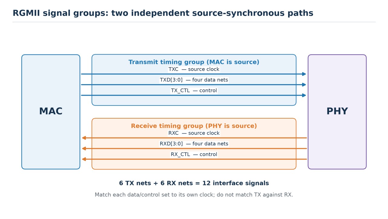
Figure 1. The MAC drives TXC, TXD[3:0] and TX_CTL; the PHY drives RXC, RXD[3:0] and RX_CTL. Each direction is a separate source-synchronous group.
RGMII v1.3 vs v2.0: The Clock Delay Question
The receiver needs clock-to-data skew so its sampling edge lands inside stable data. RGMII v1.3 does not provide the delay internally; the design must add roughly 1.5 to 2.0 ns on both directional paths, commonly through PCB clock routing. RGMII v2.0 permits internal TX and RX delay options.[4] (Microchip, Microchip Support Article) Mixed-version devices still require an end-to-end budget.
The delay may sit in the transmitter, receiver or PCB. For MAC-to-PHY traffic, aggregate MAC output timing, PCB skew and PHY input delay; reverse those roles for PHY-to-MAC traffic. Do not assume that every mode named "RGMII-ID" has identical electrical meaning.
Duplicated ownership is the dangerous case. A routed 2 ns delay plus another 2 ns in silicon can move the sample past the useful window; omitting both can leave too little setup time. Check both datasheets, strap pins, delay registers and firmware or device-tree settings. Record the delay source separately for TX and RX.
The DP83867 shows why this review is device specific: it configures transmit and receive timing independently and adjusts shifted-mode skew in 0.25 ns increments. That flexibility helps only when the schematic, registers and layout describe the same plan.
RGMII vs SGMII: Choosing the Right MAC-to-PHY Interface
RGMII and SGMII solve the same board-level connection with different physical architectures. RGMII uses 12 single-ended nets and two forwarded clocks. It needs no SERDES, but it consumes more pins and asks the PCB designer to preserve two parallel timing groups.
SGMII serializes the link. A common implementation uses one TX differential pair and one RX differential pair, runs the serial PMA at 1.25 Gbaud and recovers the clock from the data. The MAC and PHY need compatible SERDES blocks plus a suitable reference clock.[5] (NXP, NXP AN3869 Application Note) Pin count drops, and an endpoint-specific SERDES channel budget may permit a longer board path than parallel RGMII; lane configuration, coupling and reference-clock details remain device specific.
The EMI comparison is not one-dimensional. Differential signaling contains return current better when the pair geometry and reference path are controlled. A 1.25 Gbaud edge can still radiate if pair balance, return paths or connector transitions are poor. RGMII has more simultaneous single-ended edges, yet a short, well-referenced route can be entirely reasonable. Power also depends on the actual I/O cells: RGMII avoids SERDES power, while SGMII may reuse a SERDES block already active in the SoC or switch.
Choose RGMII when both devices support it directly, the separation is short, pins are available and the parallel timing budget is manageable. Choose SGMII when pin density, placement distance or the existing SERDES architecture makes the serial link easier. Verify the exact MAC and PHY modes before committing the schematic; neither interface is universally superior. Detailed SGMII differential-pair routing is outside this article.
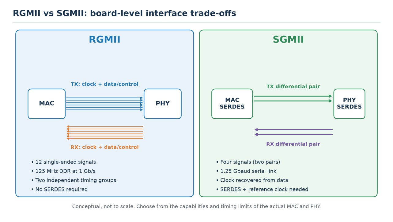
Figure 2. RGMII uses two parallel source-synchronous groups; SGMII commonly uses one TX pair and one RX pair with SERDES clock recovery.
RGMII Routing Guidelines for PCB Design
These RGMII routing guidelines for PCB design protect the timing budget through impedance control, directional grouping, deliberate clock-delay ownership, and disciplined layer transitions.
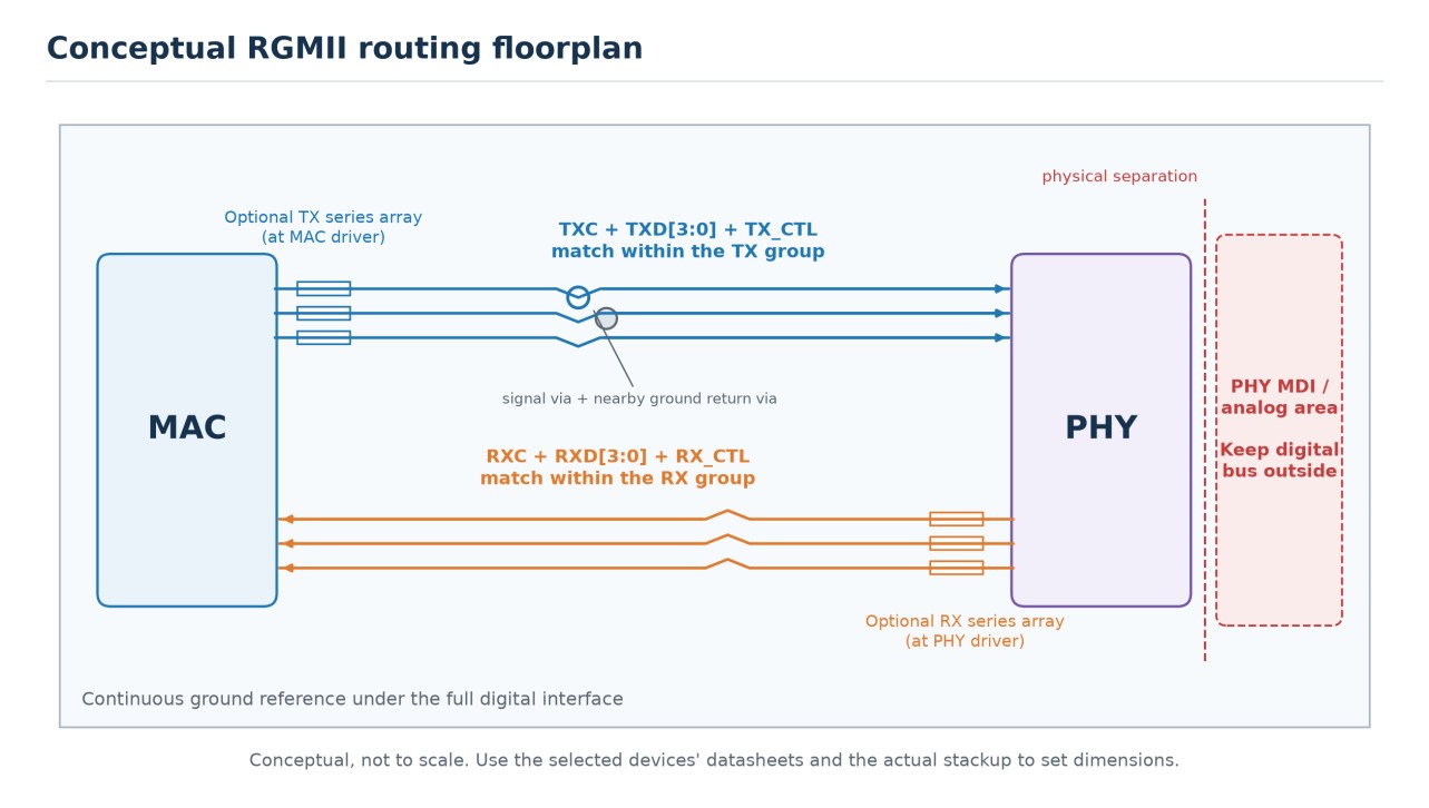
Figure 3. A practical floorplan keeps TX and RX as separate matching groups, places optional series resistors at the actual drivers and preserves a continuous return path.
Impedance and Termination
TI SNLA387 recommends 50 Ω ±10% single-ended impedance for MII-class traces, including clock and control.[6] (TI, TI SNLA387 Application Note) This is vendor guidance, not a protocol clause that guarantees every MAC and PHY is optimally terminated at exactly 50 Ω. Use the selected devices' I/O specifications and the fabricator's stackup to solve trace geometry.
Keep the reference plane continuous. A trace crossing a split forces return current around the void, increasing loop area and changing local impedance. If a signal changes layers, adjust geometry as needed because the same width does not produce the same impedance as both microstrip and stripline.
Series termination is a source-impedance decision, not a default resistor value. The external value is approximately the target line impedance minus the driver's output impedance, subject to package and load effects.[7] (Microchip, Microchip VPPD-01173 Guide) Use the datasheet or IBIS model rather than installing 22 Ω or 33 Ω everywhere because those values are common elsewhere.
Placement follows direction: TX resistors go near the MAC; RX resistors go near the PHY. Keep the pin-to-resistor segment short. Some PHYs already calibrate their output near 50 Ω; Microchip's VSC8211 guide says those outputs need no external series resistors on a 50 Ω line, while a low-impedance MAC output may require one near the MAC. The example shows why each driver needs review. To check trace widths for a target impedance in the actual stackup, start with the JLCPCB impedance calculator.
Length Matching and Grouping
Create two constraint groups in the layout tool:
- TX group: TXC, TXD[3:0] and TX_CTL, launched by the MAC.
- RX group: RXC, RXD[3:0] and RX_CTL, launched by the PHY.
Match data and control to the clock within their own direction. Cross-group matching buys nothing because TX and RX have different sources, clocks and often different internal delays.
TI SNLA387 recommends routes below 6 inches, 20 mil matching for 1 Gb/s and 50 mil for 10/100 Mb/s, with few vias and stubs. These are conservative checklist values, not universal RGMII-standard limits; device timing tables remain controlling.
Build the real constraint from a budget. One useful conceptual form is:
PCB skew allowance = available half-cycle window - transmitter uncertainty - receiver setup/hold - clock uncertainty - internal-delay variation - design margin
The smaller setup-side or hold-side result governs. Convert only that remaining time into length with the propagation delay of the actual route. TI's method subtracts internal-delay variation, transmitter skew, I/O skew and PCB skew before comparing the residual margins with receiver requirements.
A 20 mil mismatch is only a few picoseconds on ordinary interconnect, so it is distinct from the nanosecond-scale intentional clock shift. Length matching controls residual intra-group skew; clock delay moves the sampling edge. The selected delay architecture determines what the length tool should compare.
Tune only where needed. Use loose, smoothly spaced meanders rather than a dense accordion whose legs couple to each other. Avoid adding vias merely to improve a length report; electrical similarity matters more than identical database length through dissimilar layers.
Clock Delay and Skew Control
Decide the delay method during schematic review. For each direction, record the transmitter, receiver, delay source, programmed value or range, and allowed PCB mismatch. Route against that table so firmware cannot silently duplicate a delay assumed in copper.
If copper creates the skew, calculate extra length rather than copying a generic ps-per-mil value:
additional trace length = required delay / propagation delay per unit length
Use propagation delay from the actual stackup solver. At an illustrative 160 ps/in, a 1.8 ns shift requires 1800 ps / 160 ps/in = 11.25 in; 1.5 to 2.0 ns would require about 9.4 to 12.5 inches.
That much serpentine consumes area and can self-couple, so internal delay is attractive. Confirm whether the device delays clock or data, which direction it affects, its tolerance and reset behavior. The DP83867 offers independent shifted modes; another PHY may not.
Plan TXC and RXC separately. TXC travels with MAC-driven TX data; RXC travels with PHY-driven RX data. Either path may receive delay in the source, destination or board if the complete budget supports it.
On first hardware, verify more than link status. Read back the delay registers and software mode, test forced 1000 Mb/s and 100 Mb/s operation, monitor CRC and frame counters, and repeat under expected voltage and temperature corners. A clean 100 Mb/s result with errors at 1 Gb/s is consistent with an RGMII timing problem, but it is not proof; measure clocks and data at accessible points before blaming a single net.
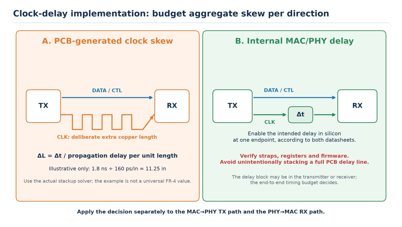
Figure 4. Budget the aggregate clock-to-data skew independently for each direction. If copper supplies the main delay, calculate its length from the actual stackup and avoid unintentionally stacking a full silicon delay.
Vias and Spacing
Minimize layer changes because each signal via adds discontinuity and complicates the return path. NXP's Ethernet layout guidance warns that through-hole vias can act as stubs and recommends reducing layer changes; TI likewise recommends minimizing vias and stubs on MII-class traces.[8] (NXP, NXP AN13335 Application Note) If a transition is unavoidable, provide a nearby ground return via when the new signal layer references another ground plane. If the reference changes between power and ground, a purpose-designed stitching capacitor may be needed instead of a ground via that does not connect the two reference conductors.
Never route the group across a plane split. Keep the TX bundle and RX bundle physically recognizable, and keep both away from switching nodes, crystals and long parallel memory routes. The objective is not a decorative bus; it is consistent impedance and low coupled noise at the receiver pins.
Spacing rules need the same attribution discipline as length rules. NXP recommends at least one trace width between adjacent xMII signals and prefers spacing based on twice the substrate height where crosstalk is a concern. TI SNLA387's 3W minimum and 5W preferred language refers to same-layer ground keepout around MII traces, not a universal 3W spacing mandate between every pair of RGMII nets. Use those vendor rules as starting points, then check the real stackup and parallel-run length. Open up spacing after dense BGA escape regions and avoid long, tightly coupled serpentines.
Keep the digital RGMII route outside the PHY's MDI and analog region. That does not require covering transformer or connector design here; it simply preserves physical separation between a fast digital bus and the sensitive media-side circuitry.
RGMII Layout Self-Check Checklist
Use this RGMII routing guidelines checklist at schematic freeze, after constraint entry and during final artwork review. Each row should resolve to evidence in the design database, device documentation or firmware configuration.
| Check Item | What to Verify | Tool/Tip |
|---|---|---|
| Controlled impedance | Every RGMII net uses the stackup geometry selected for the target single-ended impedance | Fabricator stackup and field solver; do not copy width from another board |
| TX timing group | TXD[3:0] and TX_CTL are constrained relative to TXC only | Layout group report; MAC is the source |
| RX timing group | RXD[3:0] and RX_CTL are constrained relative to RXC only | Layout group report; PHY is the source |
| Skew budget | Match tolerance follows the selected MAC/PHY timing budget; TI's 20 mil value is identified as vendor guidance | Timing worksheet plus post-route length report |
| Delay ownership | Aggregate skew budget is documented separately for TX and RX; no full PCB or silicon delay is stacked unintentionally | Check datasheets, straps, registers and device tree or firmware |
| Drive and termination | Driver strength, on-die impedance and any external series resistor agree; resistor sits at the driver | Datasheet or IBIS review; record fit/DNP choice |
| Vias and return path | Layer changes are minimized, a valid nearby return transition exists and no trace crosses a split | Plane viewer and 3D/via inspection |
| Final interference review | DRC is clean; long parallel exposure to clocks, power and memory is avoided; RGMII stays outside the MDI area | EasyEDA DRC/length tools or equivalent, followed by manual review |
FAQs about RGMII Routing
What Is the RGMII Clock Frequency?
At 1000 Mb/s, TXC and RXC run at 125 MHz and transfer data on both edges. At 100 Mb/s and 10 Mb/s, the clocks run at 25 MHz and 2.5 MHz respectively. Do not call the Gigabit clock 250 MHz; the edge transfer rate doubles, not the fundamental clock frequency.
How Tight Does RGMII Length Matching Need to Be?
There is no responsible universal answer without the MAC and PHY timing tables. TI SNLA387 recommends 20 mil intra-group matching at 1 Gb/s and 50 mil at 10/100 Mb/s, with routes under 6 inches. Use those as vendor practice unless the device-specific budget proves a different limit, and never match TX nets against RX nets.
Do RGMII Traces Need Series Resistors?
Not automatically. Compare the driver's output impedance and edge rate with the routed line, including any on-die termination or programmable drive setting. If an external source resistor is required, place it close to the driver: near the MAC for TX and near the PHY for RX.
When Should I Use SGMII Instead of RGMII?
The RGMII vs SGMII choice usually favors SGMII when pin density, placement distance or an existing SERDES architecture outweighs the power and configuration cost of the serial link. RGMII remains practical for short, direct MAC-to-PHY connections when both devices expose compatible timing controls.
Conclusion about RGMII Routing
Useful RGMII routing guidelines begin with the source-synchronous architecture, not a list of copied length numbers. Keep TX and RX as separate groups. Attribute impedance and matching limits to the vendor that published them. Decide where each directional clock delay comes from, then make the schematic, PCB constraints, straps and software express the same decision.
A layout can meet a 20 mil report and still fail if the delay is doubled, the return plane is broken or the resistor sits at the receiver. Conversely, a carefully budgeted interface does not need ornamental tuning. Give the clocks clean reference paths, control residual skew within each group and verify the programmed timing on first hardware.
The media-side channel still needs its own review before release. If the team wants outside help checking the complete layout, we provide professional PCB layout service without changing the device-specific timing work described here.
Sources:
[1] TI TIDU832A/B Reference Design — EMI/EMC-Compliant Industrial Temp Dual-Port Gigabit Ethernet Reference Design
[2] TI DP83867IR/CR Datasheet — DP83867IR/CR Datasheet
[3] TI SNLA243 Application Note — RGMII Interface Timing Budgets
[4] Microchip Support Article — Clarification on RGMII v1.3/2.0 Timing
[5] NXP AN3869 Application Note — Implementing SGMII Interfaces on the PowerQUICC III
[6] TI SNLA387 Application Note — Ethernet PHY PCB Design Layout Checklist
[7] Microchip VPPD-01173 Guide — PCB Design and Layout Guide
[8] NXP AN13335 Application Note — PCB Design Guidelines for Automotive Ethernet
Keep Learning
HDMI PCB Layout Guidelines:Impedance & Length Matching
Key Takeaways Route the four TMDS pairs as 100 Ω differential pairs, and hold that value through vias, pads, and the connector. Match the P and N traces in each pair first, then match the pairs to each other within your silicon vendor's limits. Keep a solid reference plane under the whole route. Never cross a split. Put ESD protection as close to the connector as practical, so surge current is diverted early. Check the signaling type first. TMDS matching rules do not apply to HDMI 2.1 FRL. Introductio......
RGMII Routing Guidelines for Reliable Gigabit PCB Design
Key Takeaways RGMII is a 12-signal, single-ended, source-synchronous parallel interface; its TX and RX paths are separate timing groups. Match TXD[3:0] and TX_CTL to TXC. Match RXD[3:0] and RX_CTL to RXC. Do not match TX against RX. Budget the aggregate clock-to-data skew separately in each direction, and avoid unintentionally stacking a full PCB delay with an enabled silicon delay. Treat 50 Ω ±10%, 20 mil matching and a 6 inch route limit as TI layout guidance, not universal clauses of the RGMII spec......
Ethernet PCB Routing: Guidelines for MAC, PHY, and RJ45
Key Takeaways Route every MDI pair as a 100 Ω differential transmission line with ±10% control, unless the selected PHY or cable specification requires a different target. TI recommends keeping each MDI route below 2 in and matching P to N within 20 mil for 1 Gb/s or 50 mil for 10/100 Mb/s. Keep metal out from under discrete magnetics, separate chassis ground from board ground, and preserve a continuous reference beneath the routed pairs. TI’s Ethernet-specific guidance places suitable ESD protection ......
SFP Pinout Explained: PCB Layout & Design Guide
Key Takeaways The SFP pinout follows a standard 20-pin edge connector, with dedicated pins for power, ground, differential data pairs, and I2C control signals. The Tx and Rx differential pairs carry the high-speed optical or copper signal and need controlled 100 ohm differential impedance through the entire routing path. Low-speed control pins (TX_FAULT, TX_DISABLE, MOD_ABS, LOS, Rate Select/RS1) use standard single-ended routing and don't need impedance matching. Placing the SFP cage near the board e......
DDR5 PCB Layout Guidelines: Design Rules and Best Practices
Key Takeaways DDR5 raises the stakes on layout: 1.1V rails and data rates up to 8800 MT/s leave far less margin for error than DDR4 did. Target around 40–45 Ω single-ended for DQ/CA and 80 Ω differential for CLK/DQS — exact values come from vendor guidelines — and hold them through every via and connector. Keep DQ and DQS length matching within about 5 mil per byte lane, and never route a DDR5 signal over a gap in its reference plane. Plan for 8 to 12 layers with dedicated ground references next to ev......
Via Stitching in PCB Design: A Complete Guide
Key Takeaways Via stitching bonds same-net copper across layers with repeated plated vias, most often ground, to cut high-frequency impedance between regions. A grounded via next to a signal layer transition gives return current a short local path and helps confine the field around the via. Via fences along board edges and RF cavities suppress edge radiation, but their isolation is geometry- and frequency-dependent, with no universal dB value. Keep stitching pitch at or below one-twentieth of the in-b......