HDMI PCB Layout Guidelines:Impedance & Length Matching
16 min
- Key Takeaways
- Introduction
- HDMI Signals and Their Routing Priorities
- Impedance and Routing Basics for TMDS Pairs
- HDMI Length Matching and Skew Control
- Layer Stack-Up and Grounding
- ESD Protection and Control Signal Routing
- Legacy/Current TMDS Rules vs. HDMI 2.1 FRL Layout Differences
- HDMI Layout Self-Check Checklist
- FAQs about HDMI Layout
- Conclusion about HDMI Layout
Key Takeaways
- Route the four TMDS pairs as 100 Ω differential pairs, and hold that value through vias, pads, and the connector.
- Match the P and N traces in each pair first, then match the pairs to each other within your silicon vendor's limits.
- Keep a solid reference plane under the whole route. Never cross a split.
- Put ESD protection as close to the connector as practical, so surge current is diverted early.
- Check the signaling type first. TMDS matching rules do not apply to HDMI 2.1 FRL.
Introduction
A board shows a clean picture at a low resolution. Then it drops the video or fails the eye diagram at 1080p or 4K. The schematic matches the reference design and the parts are right. The usual cause is routing: the HDMI traces were laid out like ordinary signals, and the HDMI PCB layout guidelines from the silicon vendors were not applied.
This article focuses on the routing side of HDMI rather than the pinout. It assumes the schematic and pin assignment are already done, so there are no pin tables here.
The sections below cover signal priorities, impedance, skew and length matching, stack-up, ESD placement, and what changes for HDMI 2.1. Every number comes from a public Texas Instruments (TI), Analog Devices (ADI), or STMicroelectronics document, and the source is named where the number is used.
HDMI Signals and Their Routing Priorities
HDMI signals split into two routing classes, and the split shows where to spend your effort.
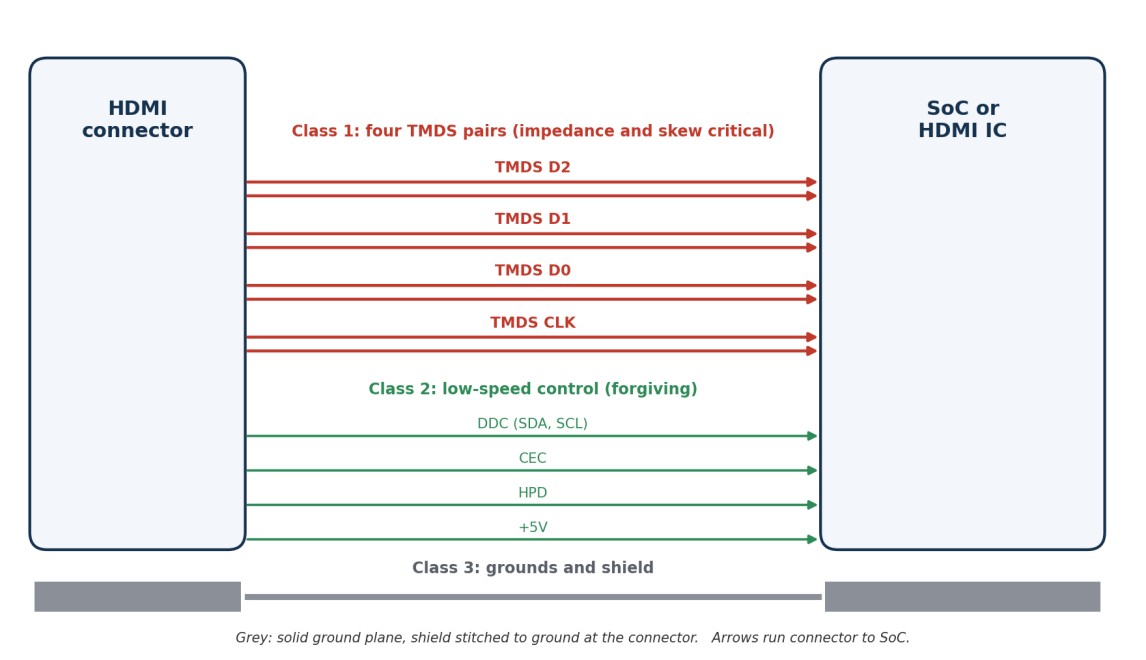
Figure 1. HDMI signal classes by routing priority: red for the four TMDS pairs, green for low-speed control signals, grey for grounds and shield.
The first class is the four TMDS differential pairs: three data channels and one clock. These are the high-speed lines, at up to 5.94 Gbps per lane for TMDS coding according to ST's HDMI application note. The drivers are current-mode and the pairs are terminated to 3.3 V at the receiving end, so impedance, skew, and the reference plane all matter. Routing freedom is close to zero: fixed impedance, matched lengths, few or no layer changes, and a short path between the connector and the IC.
The second class is the low-speed control group: DDC (an I2C-style bus), CEC, HPD, and +5V. These are single-ended nets with slow edges. They tolerate vias, layer changes, and longer routes, which is why TI places them on the bottom layer of its recommended stack. Where ARC or HEC is implemented, the utility and HPD pins take on a paired role. Route them as a low-speed pair and keep them off the TMDS layer.
Grounds and the connector shield make up a third class, and they set the return path for everything else. Spend the time on the four TMDS pairs, and keep the control group simple.
Impedance and Routing Basics for TMDS Pairs
Impedance is the first hard rule. TMDS pairs target 100 Ω differential in the TI and ADI layout guides, and that value only holds when the reference plane stays continuous under the pair. Two parts follow: how to get the number from your stack-up, and the routing habits that keep it.
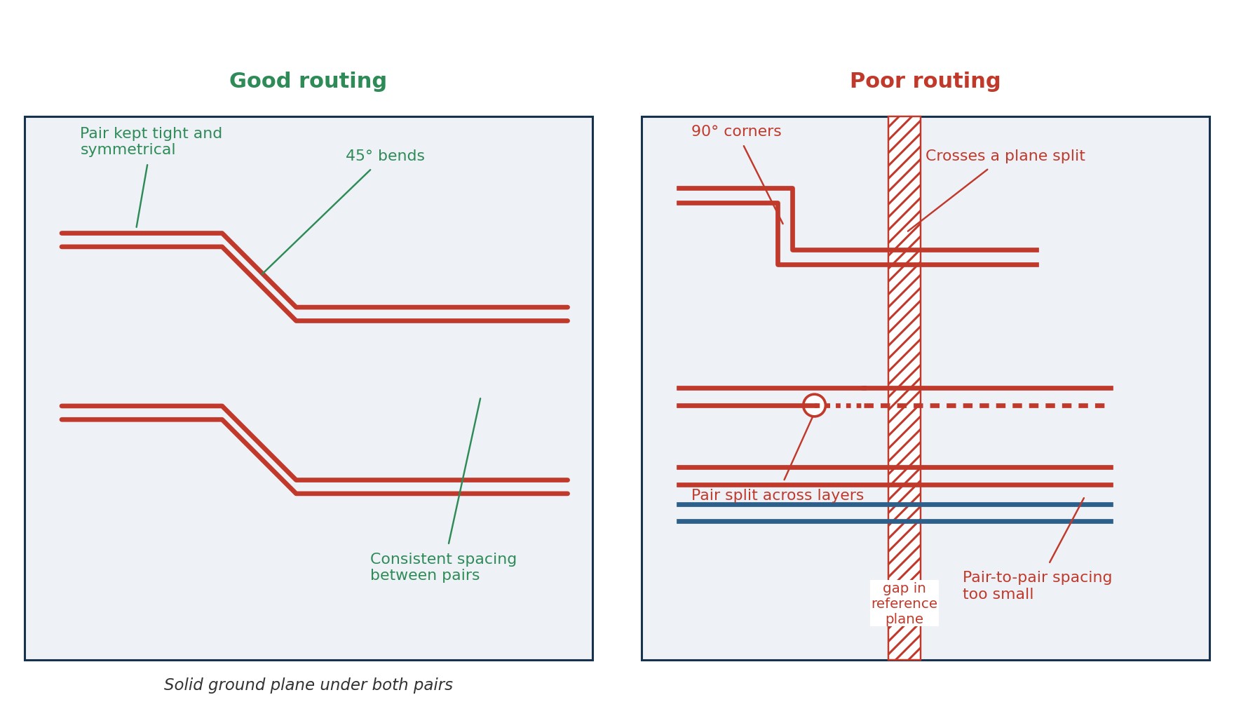
Figure 2. Good and poor TMDS routing over a reference plane, with each defect labeled.
100-Ω Differential Impedance Control
Differential impedance depends on four things: trace width, the gap between P and N, the dielectric height to the reference plane, and the dielectric constant.
Start from the stack-up your fab gives you. Enter the layer thickness and dielectric constant into an impedance calculator, such as the one built into EasyEDA, and adjust width and gap until the result is 100 Ω. TI's HDMI Design Guide adds two cautions. Closed-form equations can be off by up to ±10%, so a 2D field solver is better for final numbers. TI also advises the smallest pair spacing your fab allows, with the geometry rules s < h, s < W, W < 2h, and d > 2s. Here s is the pair gap, W the trace width, h the height to the plane, and d the distance to the next trace.
On tolerance, ADI's HDMI layout guideline asks for 100 Ω ±5% on TMDS pairs, and TI treats a deviation beyond 100 Ω ±15% as a discontinuity. Aim for the tighter figure on straight runs. Then tell the fab: mark the TMDS pairs as controlled impedance on the fabrication drawing and state 100 Ω differential, so the fab can adjust width and spacing to its own process.
Trace Routing Rules: Spacing, Reference Plane, and Vias
Most vendor HDMI layout guidelines reduce to the rules below. Each has a one-line reason.
- Keep P and N symmetrical and coupled. Constant spacing keeps impedance steady and lets the two fields cancel.
- Space pairs from other signals. ADI asks for at least 1.2 mm between TMDS pairs and 7.8 mm to non-pair signals. TI asks for at least 3 times the pair gap to a neighboring pair or shield trace. Use the value your silicon vendor gives.
- Never cross a split in the reference plane. The return current detours and couples into neighboring traces.
- Minimize layer transitions. Routing TMDS on the top layer avoids vias (TI). If a change is unavoidable, place a ground via next to the signal via when both reference planes are ground.
- Avoid 90° corners. Use chamfered bends, with a chamfer length of 3 to 5 times the trace width and 8 to 10 times the trace width between bends (ADI and TI).
- Keep vias and pads small. TI reports that oversized vias and pads can pull impedance below 85 Ω.
- Route both traces of a pair together around obstacles. Splitting the pair changes the spacing and the impedance.
HDMI Length Matching and Skew Control
Skew is a difference in arrival time. Intra-pair skew is the difference between the P and N traces of one pair. Inter-pair skew is the difference between the data pairs and the clock pair. Intra-pair skew turns part of the differential signal into common-mode noise and adds jitter through duty cycle distortion, as the ADI datasheets note. Inter-pair skew makes the bits of one pixel arrive at different times. Both close the eye.
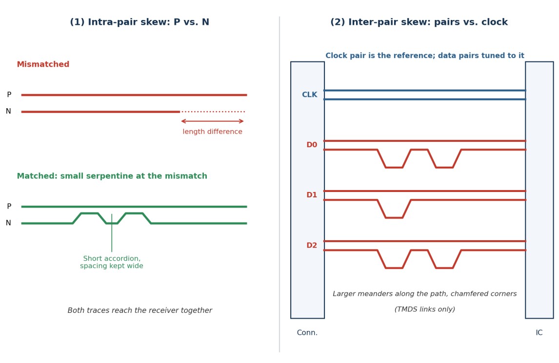
Figure 3. Intra-pair skew corrected with a small serpentine (left), and data pairs matched to the clock pair for inter-pair skew (right).
Intra-Pair Skew: Matching the P and N Traces
Match P and N more tightly than anything else in the interface. TI's guide quotes the HDMI budget as 0.4 TBIT at the receiver, which is 178 ps at a 225 MHz TMDS clock, and 0.15 TBIT at the transmitter, which is 66 ps at the same clock. As a layout rule, ADI keeps the two traces of a pair within ±3 mm.
When a pair is out of match, fix it where the mismatch starts. TI recommends small meanders at the point of mismatch, for example right after a pin or bend that shortened one trace. Keep the meander gentle, with chamfered corners and enough space between bends. Include pad and via lengths in the measurement.
Inter-Pair Skew: Matching TMDS Data Channels
HDMI length matching between channels follows the same idea at a larger scale. A pixel needs all four pairs to arrive together, so the data pairs are matched against the clock pair. ADI keeps the TMDS pairs of a channel within ±3 mm of each other. TI gives the HDMI budgets in time: 2.67 ns at the receiver and 888 ps at the transmitter for a 225 MHz TMDS clock.
Budgets tighten as data rates rise. The table shows what public vendor documents support, and where they stop.
| Link Type | Guidance | Source |
|---|---|---|
| TMDS layout rule | ±3 mm within a pair, and between the pairs of a channel | ADI HDMI layout guideline |
| TMDS, 225 MHz clock, receiver | 178 ps intra-pair, 2.67 ns inter-pair | TI HDMI Design Guide |
| TMDS, 225 MHz clock, transmitter | 66 ps intra-pair, 888 ps inter-pair | TI HDMI Design Guide |
| HDMI 2.0 (TMDS up to 5.94 Gbps per lane) | Tighter than at 225 MHz. Use the tolerance in your silicon vendor's guide. | ST AN5121 (data rate) |
| HDMI 2.1 FRL | No clock pair to match against. See the FRL section below. | Silicon vendor guide |
Tune the pairs in the order your vendor guide gives. If it gives none, tune the clock pair first and match the data pairs to it. TI suggests small corrections at the mismatch for intra-pair skew, and larger meanders along the path for inter-pair skew.
Layer Stack-Up and Grounding
Impedance and return paths are stack-up decisions, made before the first trace is routed. Two choices matter most: which layer carries the TMDS pairs, and how the ground ties together at the connector.
Choosing the Right Stack-Up for HDMI
TI recommends at least four layers for a low-EMI HDMI design. Top to bottom, the order is a TMDS signal layer, a ground plane, a power plane, and a control signal layer. Each has a reason. TMDS on the top layer avoids vias. The solid ground next to it sets the impedance and gives the return current a short path. The power plane next to ground adds high-frequency bypass capacitance. Slow control signals on the bottom layer can tolerate vias.
Ask the fab for a controlled, thin prepreg between the TMDS layer and the ground plane, since that height sets the trace width needed for 100 Ω. If more planes are needed, TI suggests adding a second power and ground pair so the stack stays symmetrical and does not warp.
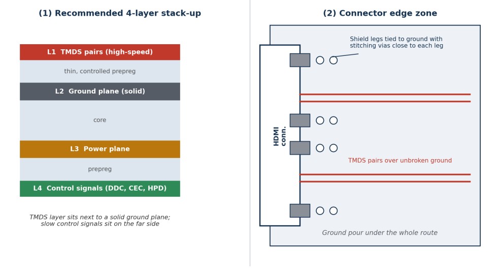
Figure 4. A recommended 4-layer stack-up with the TMDS layer next to ground (left), and shield legs tied to ground with stitching vias at the connector edge (right).
A two-layer board can work for some designs, but holding 100 Ω and a continuous return path is much harder without a nearby ground plane. If four layers are not possible, follow a vendor reference layout closely and check the result with TDR.
Grounding, Shield Connection, and Return Paths
At the connector, tie the receptacle shield legs to the ground plane with stitching vias placed close to each leg. Keep the ground plane continuous under the whole HDMI route, from the connector to the IC.
Return current follows the signal. When a pair crosses a gap, the return current detours, and TI notes that the detour couples into other traces and shifts the impedance. A layer change does the same. If the signal moves between two ground planes, add a ground via next to the signal via. If the planes are at different potentials, such as ground and power, the return path needs extra vias and a decoupling capacitor, and the added inductance hurts signal integrity. Avoid that layer change.
One exception applies at the connector pads. TI advises keeping metal out from under and between the pads where the footprint calls for it, because impedance can drop below 75 Ω and fail TDR. Follow the connector's footprint drawing.
ESD Protection and Control Signal Routing
HDMI connectors are touched by hands and cables all the time, which makes them the main entry point for ESD. Where the protection sits decides whether it works. Two parts follow: placing the ESD array, and routing the slow signals.
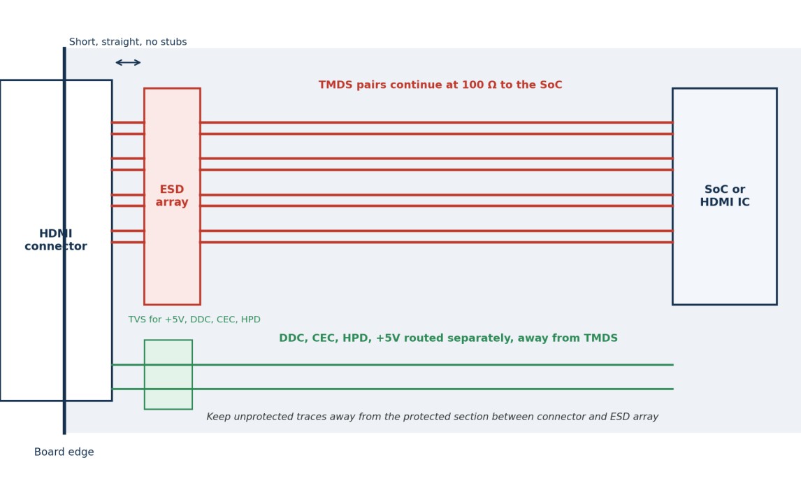
Figure 5. Plan view of the HDMI corner of a board: connector at the edge, ESD array directly behind it, TMDS pairs continuing to the SoC, control signals routed separately.
Placing ESD Protection Near the Connector
Place the ESD device as close to the HDMI connector as practical. TI notes that this simplifies routing and raises system-level ESD robustness, and ST asks for the ESD and EMI filter parts to sit as close as possible to the connector. The surge is then diverted before it travels deeper into the board. During a strike, the struck trace can also couple into nearby unprotected traces, so keep those away from the protected section.
For TMDS, use a low-capacitance array and let the pairs pass straight through it. Pick a package whose pin order matches the connector so the pairs run straight, with 45° bends where needed (TI). Do not branch a stub off the pair to reach a diode. The pair should reach 100 Ω on the PCB itself, as ST advises, without counting on the ESD part to fix it. If a via is needed between the connector and the array, route from the connector to the array pin before the via. An array placed far from the connector protects less, because the surge has already entered the board.
Routing DDC, CEC, HPD, and +5V
The low-speed signals forgive a lot, but they still need discipline. Route DDC, CEC, and HPD as ordinary single-ended nets. Place the pull-up resistors where the silicon vendor's reference design puts them, since the value and location depend on the part. Keep these nets out of the TMDS zone and off the TMDS layer. At the connector, protect the non-TMDS pins with a TVS rated for 5 V operation, as TI's ESD application brief shows for +5V, SDA, SCL, HPD, and CEC.
The +5V pin has a job of its own: the source must supply the current the HDMI specification requires. Size the trace or pour and its protection for that current, and check the figure against your vendor's reference design.
Legacy/Current TMDS Rules vs. HDMI 2.1 FRL Layout Differences
The routing rules in this article assume TMDS, which covers designs up to HDMI 2.0. HDMI 2.1 adds Fixed Rate Link, or FRL, and the layout priorities change with it.
FRL removes the dedicated clock channel. The clock is embedded in the data, and the former clock pair carries a fourth data lane. Each lane runs at up to 12 Gbps, for up to 48 Gbps in total, as ST's application note lists for HDMI 2.1b. With no clock pair, clock-to-data matching no longer applies. The work shifts to channel loss, via discontinuities, the insertion loss budget, and skew inside each lane.
At FRL rates the insertion loss budget tightens sharply, vias matter more, and intra-lane skew tolerances shrink. When the loss budget is hard to meet, designers usually compare three options: a shorter route, a lower-loss laminate, or a redriver or retimer from the silicon vendor. For HDMI 2.1 products, follow the silicon vendor's layout guide and characterization data. The official HDMI specification is a licensed document, so it is not quoted here, and no FRL tolerances are given that public vendor documents do not support.
HDMI Layout Self-Check Checklist
| Check Item | What to Verify |
|---|---|
| Pair impedance | 100 Ω differential on all four TMDS pairs against your fab stack-up, with a controlled-impedance note on the fab drawing |
| Intra-pair skew | P and N lengths within the vendor budget (ADI's guideline uses ±3 mm), counting pads and vias |
| Inter-pair skew | Pairs matched as the silicon vendor specifies. TMDS designs are matched to the clock, and FRL designs follow the vendor guide |
| Reference plane | No splits, slots, or voids under any HDMI trace, from the IC to the connector |
| Layer changes | Few vias, small pads, and a ground via next to every signal via that changes reference plane |
| Corners and spacing | No 90° corners, pair spacing per the vendor, control signals kept clear of TMDS |
| ESD placement | Array at the connector, short path with no stubs, low-capacitance type on the TMDS pairs |
| Shield and DRC | Stitching vias at the shield legs, and a DRC pass with differential-pair rules enabled |
FAQs about HDMI Layout
Q1: What impedance should HDMI TMDS pairs use?
HDMI TMDS pairs are typically designed for 100 Ω differential impedance. ADI's layout guideline asks for ±5% on the pairs, and the exact tolerance and implementation should follow the relevant HDMI specification and your silicon vendor's guidance.
Q2: How long can HDMI traces be on a PCB?
The HDMI specification does not set a maximum trace length, only the expected impedance, according to ADI. ADI also states that runs of 20 to 30 cm are easy when the layout rules are followed. Shorter is better as data rates rise, and FRL designs need a loss budget check.
Q3: What is the length matching tolerance for HDMI?
HDMI length matching depends on the link type. For TMDS, ADI's guideline uses ±3 mm within a pair and between pairs, and TI gives time budgets at a 225 MHz clock. For HDMI 2.0, use the tolerance in your silicon vendor's guide. For HDMI 2.1 FRL there is no clock pair, so matching applies inside each lane, per the vendor's guide.
Q4: Can I route HDMI on a two-layer board?
Yes, but it is harder. TI recommends at least four layers for a low-EMI HDMI design. On two layers there is no close ground plane, so 100 Ω pairs come out wide and the return path is harder to control. Keep the run short, keep the pairs on one layer over a continuous ground pour on the other, and confirm the result with a TDR measurement.
Conclusion about HDMI Layout
Reliable HDMI is decided in layout. Impedance, matching, reference planes, and ESD placement need to be right the first time.
The HDMI PCB layout guidelines in this article come down to a priority order. First, sort the signals into classes and put the effort on the TMDS pairs. Second, hold 100 Ω differential impedance. Third, match lengths within each pair and between pairs, or follow the vendor guide if the design uses HDMI 2.1 FRL. Fourth, choose a stack-up with a solid ground next to the TMDS layer. Fifth, place ESD protection at the connector.
Run the checklist above before the files go to fabrication. If you would rather hand off the layout work, JLCPCB's PCB design and layout services can take it from there: upload your schematic, and our engineers will handle the routing, impedance planning, and stack-up.
Keep Learning
HDMI PCB Layout Guidelines:Impedance & Length Matching
Key Takeaways Route the four TMDS pairs as 100 Ω differential pairs, and hold that value through vias, pads, and the connector. Match the P and N traces in each pair first, then match the pairs to each other within your silicon vendor's limits. Keep a solid reference plane under the whole route. Never cross a split. Put ESD protection as close to the connector as practical, so surge current is diverted early. Check the signaling type first. TMDS matching rules do not apply to HDMI 2.1 FRL. Introductio......
RGMII Routing Guidelines for Reliable Gigabit PCB Design
Key Takeaways RGMII is a 12-signal, single-ended, source-synchronous parallel interface; its TX and RX paths are separate timing groups. Match TXD[3:0] and TX_CTL to TXC. Match RXD[3:0] and RX_CTL to RXC. Do not match TX against RX. Budget the aggregate clock-to-data skew separately in each direction, and avoid unintentionally stacking a full PCB delay with an enabled silicon delay. Treat 50 Ω ±10%, 20 mil matching and a 6 inch route limit as TI layout guidance, not universal clauses of the RGMII spec......
Ethernet PCB Routing: Guidelines for MAC, PHY, and RJ45
Key Takeaways Route every MDI pair as a 100 Ω differential transmission line with ±10% control, unless the selected PHY or cable specification requires a different target. TI recommends keeping each MDI route below 2 in and matching P to N within 20 mil for 1 Gb/s or 50 mil for 10/100 Mb/s. Keep metal out from under discrete magnetics, separate chassis ground from board ground, and preserve a continuous reference beneath the routed pairs. TI’s Ethernet-specific guidance places suitable ESD protection ......
SFP Pinout Explained: PCB Layout & Design Guide
Key Takeaways The SFP pinout follows a standard 20-pin edge connector, with dedicated pins for power, ground, differential data pairs, and I2C control signals. The Tx and Rx differential pairs carry the high-speed optical or copper signal and need controlled 100 ohm differential impedance through the entire routing path. Low-speed control pins (TX_FAULT, TX_DISABLE, MOD_ABS, LOS, Rate Select/RS1) use standard single-ended routing and don't need impedance matching. Placing the SFP cage near the board e......
DDR5 PCB Layout Guidelines: Design Rules and Best Practices
Key Takeaways DDR5 raises the stakes on layout: 1.1V rails and data rates up to 8800 MT/s leave far less margin for error than DDR4 did. Target around 40–45 Ω single-ended for DQ/CA and 80 Ω differential for CLK/DQS — exact values come from vendor guidelines — and hold them through every via and connector. Keep DQ and DQS length matching within about 5 mil per byte lane, and never route a DDR5 signal over a gap in its reference plane. Plan for 8 to 12 layers with dedicated ground references next to ev......
Via Stitching in PCB Design: A Complete Guide
Key Takeaways Via stitching bonds same-net copper across layers with repeated plated vias, most often ground, to cut high-frequency impedance between regions. A grounded via next to a signal layer transition gives return current a short local path and helps confine the field around the via. Via fences along board edges and RF cavities suppress edge radiation, but their isolation is geometry- and frequency-dependent, with no universal dB value. Keep stitching pitch at or below one-twentieth of the in-b......