SFP Pinout Explained: PCB Layout & Design Guide
15 min
- Introduction
- What Is an SFP Connector and How Does It Work?
- SFP Pinout: Complete 20-Pin Reference
- SFP Connector Schematic Design Essentials
- PCB Layout Guidelines for SFP Connectors
- SFP Cage Design Considerations
- Common SFP Layout Mistakes to Avoid
- FAQs about SFP Pinout
- Conclusion about SFP Pinout
Key Takeaways
- The SFP pinout follows a standard 20-pin edge connector, with dedicated pins for power, ground, differential data pairs, and I2C control signals.
- The Tx and Rx differential pairs carry the high-speed optical or copper signal and need controlled 100 ohm differential impedance through the entire routing path.
- Low-speed control pins (TX_FAULT, TX_DISABLE, MOD_ABS, LOS, Rate Select/RS1) use standard single-ended routing and don't need impedance matching.
- Placing the SFP cage near the board edge, keeping high-speed pairs on inner layers, and holding a continuous reference plane are the core layout rules.
- SFP+ and SFP28 share the same 20-pin mechanical footprint as SFP but push higher data rates, which tightens layout tolerances considerably.
Introduction
Selecting the wrong SFP module footprint, or getting the SFP pinout wrong on a schematic, is a common source of dead-on-arrival optical links. Sometimes the transceiver simply refuses to initialize. Other times it links up fine on the bench, then throws bit errors the moment traffic ramps up, and the fault traces straight back to a misrouted differential pair or a missing pull-up on a control pin.
Understanding the SFP pinout matters because the SFP connector packs power, ground, high-speed data, and low-speed control signals into a single 20-pin edge interface. A PCB layout engineer needs to know which pins carry gigabit-per-second data and which just toggle a status flag, since the two demand completely different routing treatment.
This guide walks through the SFP connector interface pin by pin, then covers the schematic and layout practices that keep a transceiver design working: impedance control, power integrity, cage placement, and the mistakes that most often trip up a first layout.
What Is an SFP Connector and How Does It Work?
Figure 1. M.2 (NGFF) SSD connector socket for SMT mounting.
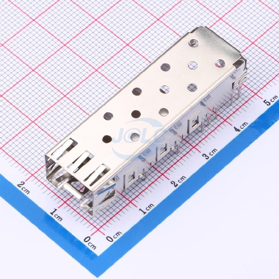
Figure 2. Single-port SFP metal cage for SMT mounting.
An SFP connector is the card-edge interface between a Small Form-factor Pluggable transceiver module and a host PCB. The module plugs into a metal cage soldered to the board, and its edge contacts land directly on 20 gold-plated pads on the host PCB. No separate connector part is needed on the module side.
Behind that simple mechanical interface sits everything a PCB designer needs to route correctly: power and ground return paths, a differential transmit pair, a differential receive pair, and a two-wire I2C bus plus a handful of status and control lines. Before laying out a single trace, it pays to know exactly what each of those 20 pins does.
SFP Connector Types and Variants
SFP started as a 1 Gbps to 4 Gbps form factor, and the family has grown considerably since. SFP+ extends the same 20-pin footprint to 10 Gbps, and SFP28 pushes it further to 25 Gbps, both keeping the mechanical layout and pin assignment essentially unchanged from the original SFP. XFP is a separate, earlier 10 Gbps form factor with its own connector and pinout, not an SFP variant, despite the similar name.
SFP and QSFP move in different directions from there. QSFP and QSFP-DD pack four, or eight for QSFP-DD, lanes into one module, aimed at 40 Gbps, 100 Gbps, and higher aggregate throughput. The pin count and connector geometry differ from SFP, but the underlying layout principles, impedance control, decoupling, and reference plane continuity, carry over directly. For most designers, the 20-pin SFP/SFP+ footprint is the one worth learning first, since it forms the basis for nearly every later generation.
SFP Pinout: Complete 20-Pin Reference
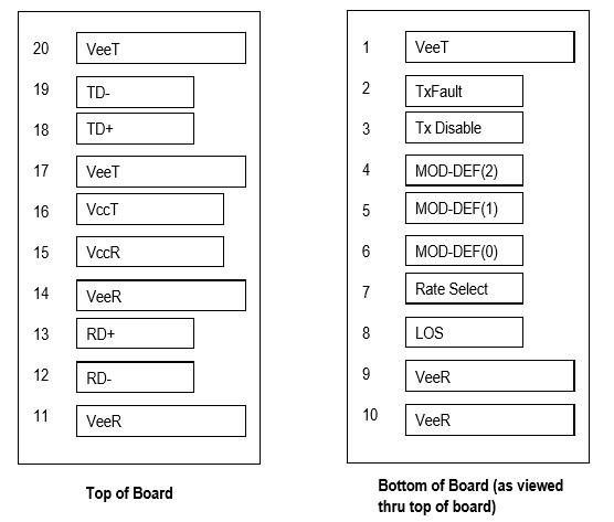
Figure 3. Complete SFP pinout table with columns for pin number, name, and function, highlighting power, ground, differential pairs, and I2C control pins.
The table below lists the standard SFP module pinout as defined by the SFP MSA. This same 20-pin arrangement carries over to SFP+ and SFP28 modules.
| Pin | Name | Function |
|---|---|---|
| 1 | VeeT | Transmitter ground |
| 2 | TX_FAULT | Transmitter fault indication (output) |
| 3 | TX_DISABLE | Disables the transmitter (input) |
| 4 | MOD_DEF2 (SDA) | I2C data line |
| 5 | MOD_DEF1 (SCL) | I2C clock line |
| 6 | MOD_DEF0 (MOD_ABS) | Module present; pulled low by the module when seated |
| 7 | Rate Select | Rate Select (SFP: RX bandwidth; SFP+: RS0) |
| 8 | LOS | Loss of signal indication (output) |
| 9 | VeeR | Receiver ground |
| 10 | VeeR | Receiver ground |
| 11 | VeeR | Receiver ground |
| 12 | RD- | Receiver data, inverting |
| 13 | RD+ | Receiver data, non-inverting |
| 14 | VeeR | Receiver ground |
| 15 | VccR | Receiver power (+3.3V) |
| 16 | VccT | Transmitter power (+3.3V) |
| 17 | VeeT | Transmitter ground |
| 18 | TD+ | Transmitter data, non-inverting |
| 19 | TD- | Transmitter data, inverting |
| 20 | VeeT | Transmitter ground |
The pinout breaks down into four functional groups. Power and ground pins, VccR, VccT, and VeeR/VeeT ground pins, make up the bulk of the 20 contacts, which reflects how much of the SFP pinout is dedicated to a clean, low-inductance return path rather than signal. The differential pairs, TD+/TD- for transmit and RD+/RD- for receive, carry the actual gigabit data and are the only pins on this connector that need controlled-impedance routing.
The I2C interface, MOD_DEF2 (SDA) and MOD_DEF1 (SCL), lets the host read the module's identification EEPROM and, on DOM-capable modules, monitor temperature, voltage, and optical power in real time. This pair uses standard slow-speed I2C routing, with no differential matching required.
The remaining control and status pins, TX_DISABLE, TX_FAULT, MOD_ABS, LOS, and Rate Select, are simple digital signals defined by the base SFP MSA. TX_DISABLE and Rate Select are host outputs into the module; TX_FAULT, LOS, and MOD_ABS are module outputs the host reads. In the original SFP MSA (INF-8074i), Pin 7 is named "Rate Select" and controls receiver bandwidth, while Pin 9 is VeeR (receiver ground). In the SFP+ MSA (SFF-8431), Pin 7 is renamed "RS0" (Rate Select 0, controlling receiver rate) and Pin 9 is repurposed as "RS1" (Rate Select 1, controlling transmitter rate). Because Pin 9 in classic SFP modules is internally connected to VeeR, an SFP+ host utilizing RS1 must provide short circuit protection to avoid damage when a legacy SFP module is inserted. None of these need anything beyond standard single-ended routing with a pull-up or pull-down as required by the module vendor's application note.
SFP Connector Schematic Design Essentials
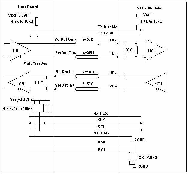
Figure 4. Minimal SFP circuit with decoupling on VccR/VccT, pull-up/pull-down resistors on control pins, and AC coupling caps on the Tx/Rx pairs.
A working SFP interface needs only a small amount of supporting circuitry beyond the connector itself, but skipping any of it invites trouble. Start with decoupling: place a 0.1 uF ceramic capacitor from VccR to VeeR and another from VccT to VeeT, positioned as close to the connector pins as the layout allows. These absorb the fast current transients the transceiver draws during switching and keep the SFP module pinout's power pins clean.
The configuration pins need pull resistors sized to the module vendor's recommendation. TX_DISABLE has an internal 4.7K to 10K ohm pull-up resistor inside the module, which keeps the transmitter disabled by default. The host typically adds an external pull-down to enable the transmitter; if the host GPIO is left floating during power-up, the internal pull-up ensures TX_DISABLE stays high (transmitter off) until explicitly driven low. RS0 and RS1 usually pull to a fixed logic level unless the design actively switches data rates. MOD_ABS needs a pull-up on the host side (typically 4.7K to 10K ohm to VccT or VccR), since the module pulls it low once seated to indicate presence.
AC coupling capacitors on the TD+/TD- and RD+/RD- pairs are optional. Many SFP modules already include on-board AC coupling, but adding 100 nF series capacitors on the host side is a low-cost way to guard against DC offset mismatch. If the exact capacitor value isn't finalized yet, populating a 0-ohm resistor as a placeholder keeps the option open for later signal integrity tuning without a board re-spin.
PCB Layout Guidelines for SFP Connectors
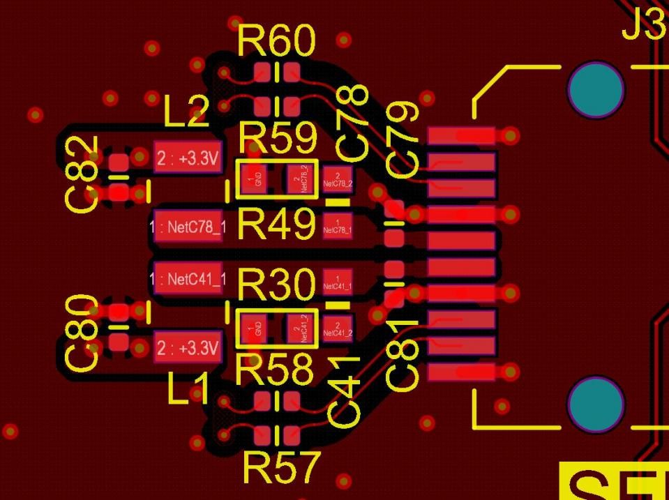
Figure 5. PCB layout detail showing power filtering inductors and decoupling capacitors on the +3.3V SFP supply nets.
SFP layout is a high-speed design problem wearing a low-speed connector's clothing. The differential pairs need the same discipline as any multi-gigabit interface: connector placement near the board edge to minimize trace length, high-speed and low-speed signals kept apart on separate layers where possible, and via transitions treated as a deliberate design decision rather than an afterthought. Getting return current management right underneath the SFP cage matters just as much as the trace geometry itself.
Impedance Control for Differential Pairs
TD+/TD- and RD+/RD- each need 100 ohm differential impedance held consistently from the SFP connector pad to the host SerDes or PHY. Start by setting trace width and pair spacing in a 2D field solver against your actual stackup, plugging in real copper weight and dielectric constant rather than rule-of-thumb numbers.
Layer stackup choice affects how achievable that target is. A pair routed on an outer layer sees a different reference environment than one on an inner layer, and switching layers mid-route changes the effective impedance unless the transition is compensated. Keep each differential pair on a single layer for its full run whenever routing density allows.
Via transitions are the other common failure point. Every via adds parasitic capacitance that pulls impedance down locally. Oversized antipads around the via barrel reduce that capacitance and help hold the 100 ohm target through the transition. Model the via in the same field solver used for the traces, and don't assume a default antipad size from the fab's stackup file is correct for a 10G+ SFP+ or SFP28 link.
Signal Routing and Return Current Management
High-speed return current follows the path of least impedance, which under normal conditions is the plane directly beneath the signal trace, not the shortest physical route back to the source. Any gap, slot, or plane split under a TD or RD pair forces that return current to detour, and the detour shows up as a controlled-impedance discontinuity even though the trace itself looks fine.
Keep the reference plane solid and unbroken under every SFP differential pair, from the connector footprint through to the SerDes. Where a signal must change layers, place a ground via close to the signal via, typically within 20 to 30 mil, so return current has a short path between the two reference planes rather than radiating from the via transition. Via stitching around the connector's ground pins ties the planes together and keeps the whole return path low-impedance.
For a broader look at routing high-speed differential pairs and managing return paths on multi-layer boards, our guide to high-speed PCB routing techniques covers the underlying principles in more depth.
Power Integrity for SFP Modules
Most SFP and SFP+ optical transceivers draw around 1 to 1.5W, with some long-reach ZR modules reaching closer to 2W. That's modest next to newer form factors, QSFP-DD modules can pull 12W or more, but it's still enough that sloppy power delivery causes real problems, particularly on the laser bias current inside the module.
Bulk decoupling, a few microfarads, handles slower load transients, while a 0.1 uF capacitor placed within a few millimeters of VccT and VccR handles fast switching noise. Some designs add a small pi filter, an inductor or ferrite bead flanked by two capacitors, between the main 3.3V rail and the SFP power pins to further isolate transceiver noise from the rest of the board. Pi filters help, but an oversized inductor can create a resonant peak in the PDN that makes noise worse at a specific frequency, so check the filter's impedance response rather than assuming more filtering is always better.
Beyond that, SFP power delivery follows standard high-speed digital PDN principles: solid planes, short loops, and decoupling sized in tiers from bulk to high-frequency. The SFP pinout's five ground pins exist specifically to give that return current multiple short paths back to the source. For more on structuring power and ground planes for a clean PDN, see ultimate guide to circuit board ground and power plane design.
SFP Cage Design Considerations
An SFP cage is the metal shell that surrounds the connector on the host PCB, providing the mechanical guide rails a module slides into and the shielding that keeps EMI contained during hot-swap operation. The cage solders to the board through its own ground tabs, which should land on a solid ground pour rather than a fragmented one.
Cage and connector alignment matters more than it might seem. Even a small mechanical offset between the cage opening and the 20-pin connector pads can cause intermittent contact or extra insertion force on the module. Follow the cage manufacturer's recommended PCB footprint exactly rather than adapting a similar part's outline.
The cage's metal body also acts as a heatsink path for the module, drawing heat away through its mounting tabs, which matters more on SFP+ and SFP28 designs running warmer than the original SFP spec. Not every design needs a full cage for mechanical stability, some low-volume or fixed-installation designs use lighter guide structures, but a proper cage remains the standard choice for any hot-swappable port.
Common SFP Layout Mistakes to Avoid
A handful of recurring layout mistakes account for most SFP interface failures, and each one is straightforward to catch during design review.
Routing the TD/RD pairs across a plane split. This is one of the most common causes of SFP connector signal integrity failures that pass initial power-on testing but fail once real traffic starts flowing. Check every differential pair's route against the reference plane layer for gaps, mounting holes, or plane-split boundaries.
Skipping decoupling on VccR or VccT. A module that initializes but throws intermittent faults under traffic load often traces back to missing or undersized decoupling right at the connector's power pins.
Leaving TX_DISABLE without a proper pull-down. The module has an internal 4.7K to 10K ohm pull-up on TX_DISABLE, which keeps the transmitter disabled until the host actively drives the pin low. If the host GPIO floats during power-up without an external pull-down to reinforce the intended state, the transmitter remains off or enters an unpredictable state until the host firmware explicitly enables it.
Mismatching intra-pair length on TD+/TD- or RD+/RD-. Even a small skew between the two traces in a differential pair degrades the eye at higher data rates. Keep intra-pair length matching tight, and hold it consistently through every via and connector footprint, not just on the straight sections.
FAQs about SFP Pinout
1. What is the difference between SFP and SFP+ pinout?
SFP and SFP+ share the identical 20-pin mechanical footprint, but there are two key differences. First, Pin 7 is named "Rate Select" in the original SFP MSA (INF-8074i) and "RS0" in the SFP+ MSA (SFF-8431). Second, Pin 9 is VeeR (receiver ground) in SFP, but repurposed as RS1 (transmitter rate select) in SFP+. The differential pair pin assignment (TD+/TD- and RD+/RD-) remains the same. SFP+ pushes the same TD/RD pairs to 10 Gbps, which tightens impedance and length-matching tolerances considerably, even though the SFP pinout table itself looks nearly identical.
2. Do I need AC coupling capacitors on SFP differential pairs?
Often not, since many SFP modules already include on-board AC coupling. Adding host-side series capacitors on TD/RD is still common practice as a low-cost safeguard against DC offset mismatch between the host and module.
3. What impedance should SFP differential pairs be routed at?
100 ohm differential impedance, held consistently through the connector pad, trace, and any via transitions between the SFP connector and the host SerDes.
4. How do I choose between SFP and QSFP for my design?
SFP and QSFP both rely on similar layout principles, but SFP targets a single-lane link up to roughly 25 Gbps with SFP28, while QSFP packs four lanes for 40 Gbps and above. Choose based on required port density and aggregate bandwidth rather than layout complexity alone.
Conclusion about SFP Pinout
Understanding the SFP pinout is the foundation for any PCB layout involving optical or copper transceivers. Once the 20 pins are sorted into their functional groups, power and ground, the TD/RD differential pairs, the I2C bus, and the status/control lines, the layout work becomes a matter of applying the right rules to each group rather than treating the whole connector as one undifferentiated interface.
The pieces that matter most: hold 100 ohm differential impedance on the high-speed pairs, keep the reference plane solid underneath them, decouple VccR and VccT close to the pins, and give the SFP cage a clean ground connection. Get those right and most SFP interface problems never show up in the first place.
If a design is pushing into SFP28 or higher data rates, or the stackup and routing plan for the connector need a second look before fabrication, JLCPCB's PCB layout services can review the routing and impedance while changes are still easy to make.
Keep Learning
SFP Pinout Explained: PCB Layout & Design Guide
Key Takeaways The SFP pinout follows a standard 20-pin edge connector, with dedicated pins for power, ground, differential data pairs, and I2C control signals. The Tx and Rx differential pairs carry the high-speed optical or copper signal and need controlled 100 ohm differential impedance through the entire routing path. Low-speed control pins (TX_FAULT, TX_DISABLE, MOD_ABS, LOS, Rate Select/RS1) use standard single-ended routing and don't need impedance matching. Placing the SFP cage near the board e......
DDR5 PCB Layout Guidelines: Design Rules and Best Practices
Key Takeaways DDR5 raises the stakes on layout: 1.1V rails and data rates up to 8800 MT/s leave far less margin for error than DDR4 did. Target around 40–45 Ω single-ended for DQ/CA and 80 Ω differential for CLK/DQS — exact values come from vendor guidelines — and hold them through every via and connector. Keep DQ and DQS length matching within about 5 mil per byte lane, and never route a DDR5 signal over a gap in its reference plane. Plan for 8 to 12 layers with dedicated ground references next to ev......
Via Stitching in PCB Design: A Complete Guide
Key Takeaways Via stitching bonds same-net copper across layers with repeated plated vias, most often ground, to cut high-frequency impedance between regions. A grounded via next to a signal layer transition gives return current a short local path and helps confine the field around the via. Via fences along board edges and RF cavities suppress edge radiation, but their isolation is geometry- and frequency-dependent, with no universal dB value. Keep stitching pitch at or below one-twentieth of the in-b......
Crosstalk in PCB Design: Causes, Types, and How to Reduce It
Key Takeaways Crosstalk starts at an edge: a changing aggressor voltage and current produce electric and magnetic fields that couple energy into a neighboring victim trace. Edge rate matters more than clock frequency alone. A modest-rate bus with fast I/O edges can still create a serious coupling problem. More spacing and a smaller signal-to-reference-plane distance usually provide the cleanest layout improvements, but the result depends on the complete cross-section. NEXT and FEXT do not scale in the......
Mastering IC Board Design: Layout Rules & Best Practices
Key Takeaways Placement is the foundation of good layout. Position ICs, decoupling capacitors, and crystals to minimize trace lengths before routing anything — placement quality determines most of your signal performance. Respect the physics, not just the schematic. High-speed designs demand controlled impedance (e.g., 90-ohm USB differential pairs), length matching, and a well-planned layer stackup to prevent reflections, crosstalk, and power noise. Handle power and heat deliberately. Size power trac......
LVDS PCB Layout Guidelines: Design Tips and Worked Example
Key Takeaways 100 Ω Differential Impedance: LVDS PCB layout starts with one number: 100 Ω of differential impedance. Trace width, spacing, and board thickness all set that number. Route Pairs Together: Route the two traces of a pair together, side by side, and keep their lengths within 5 to 10 mil of each other. Solid Ground Plane: Never let an LVDS pair cross a gap in the ground plane. It breaks the return path and hurts the signal. 4-Layer Minimum: A 4-layer board with a solid ground plane is enough......