Ethernet PCB Routing: Guidelines for MAC, PHY, and RJ45
17 min
- Introduction
- Ethernet Circuit Basics: MAC, PHY, and Magnetics
- Gigabit Ethernet PCB Layout Guidelines: Placement and Stackup
- Ethernet Transformer Routing: MDI Differential Pairs
- Ethernet Length Matching Tolerance
- EMI, ESD, and Common Mistakes in Ethernet Routing
- Ethernet Routing Self-Check Checklist
- FAQs About Ethernet PCB Routing
Key Takeaways
- Route every MDI pair as a 100 Ω differential transmission line with ±10% control, unless the selected PHY or cable specification requires a different target.
- TI recommends keeping each MDI route below 2 in and matching P to N within 20 mil for 1 Gb/s or 50 mil for 10/100 Mb/s.
- Keep metal out from under discrete magnetics, separate chassis ground from board ground, and preserve a continuous reference beneath the routed pairs.
- TI’s Ethernet-specific guidance places suitable ESD protection on the PHY side of the magnetics.
- Treat every generic rule as a starting point. The PHY, magnetics, connector, protection-device, and PoE datasheets govern the finished design.
Introduction
A Gigabit link can look clean on a short bench cable and still drop packets, radiate badly, or reset when a production cable is attached. Careful Ethernet PCB routing reduces those risks before the first board is fabricated. The vulnerable path is compact: PHY pins, balanced MDI pairs, isolation magnetics, cable-side termination, chassis interface, and RJ45.
The layout must hold differential impedance while controlling common-mode conversion, return paths, crosstalk, and surge-current geometry. Those concerns are coupled. Moving a ground pour can change impedance; adding a via can unbalance a pair; routing over a split can turn a nominally differential current into a larger radiating loop.
This guide covers the PHY-to-RJ45 channel. The MAC-to-PHY digital interface is mentioned only for context because its clocking and skew rules belong in a separate companion article.
Ethernet Circuit Basics: MAC, PHY, and Magnetics
An Ethernet circuit has three functional regions on the board: the MAC, the PHY, and the cable interface. The MAC exchanges frames with the system processor. The PHY converts that digital traffic into the signaling used on the physical medium. Magnetics and the RJ45 couple that signaling to the cable while separating the local electronics from the external network.
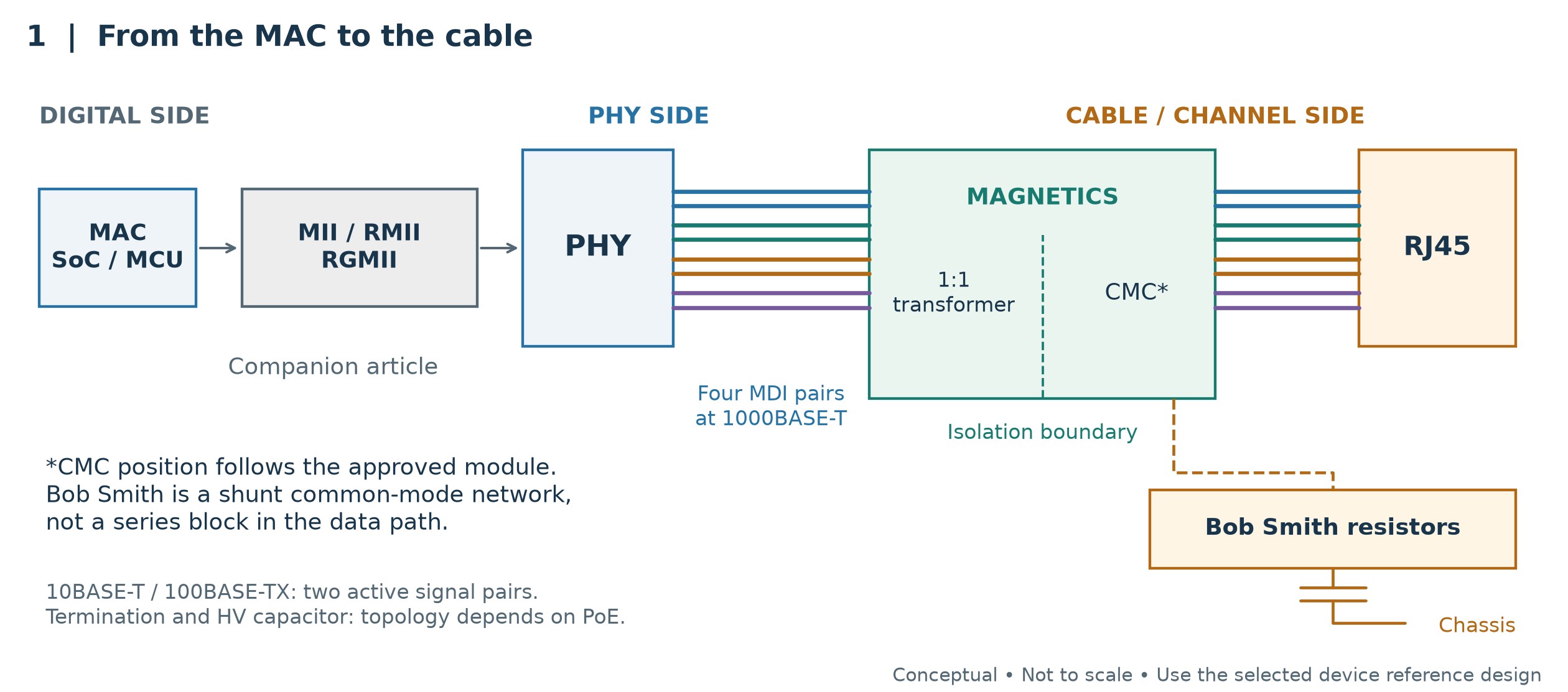
Figure 1. Signal chain from the MAC to the RJ45; this guide concentrates on the PHY-to-connector channel.
From MAC to PHY: The Digital Interface
The MAC, often inside the processor, handles Ethernet frames; the PHY transmits and recovers the cable signal. MII, RMII, and RGMII are parallel MAC-to-PHY interface options, with support depending on speed and device.[1] (Texas Instruments, SimpliPHY Your Ethernet Design, Part 1: Ethernet PHY Basics and Selection Process) Their routing belongs in the companion rgmii routing guidelines; the MDI pairs discussed here carry the analog cable signaling.
Magnetics and Isolation: Why the Transformer Exists
Ethernet magnetics are the electrical boundary between the board and the cable. A PHY-approved module commonly combines a 1:1 isolation transformer with common-mode filtering. The transformer provides galvanic isolation and balanced coupling; the common-mode choke attenuates noise that would otherwise leave on the cable or enter the receiver.[2] (Microchip Technology, Magnetics Guide) IEEE isolation performance must be met, but the standard does not require one universal magnetic topology. Component selection therefore starts with the PHY reference design and the magnetics datasheet, not a generic schematic copied from another board.
Cable-side center taps or spare-pair nodes may use a Bob Smith termination to absorb common-mode energy. A familiar implementation uses 75 Ω resistors whose common node is AC-coupled to chassis, but that value and connection are not universal. PoE changes the termination arrangement, and one vendor guide explicitly distinguishes the high-voltage chassis capacitor from the Bob Smith resistor network itself.[3] (Texas Instruments, AN-1469 PHYTER Design & Layout Guide) Check the selected PHY, magnetics, connector, and PoE architecture before fixing values or net names.
Gigabit Ethernet PCB Layout Guidelines: Placement and Stackup
Placement makes the routing easy or forces compromises into every pair. These Gigabit Ethernet PCB layout guidelines start at the board edge and work inward, then use the stackup to give the short channel a stable electromagnetic environment.
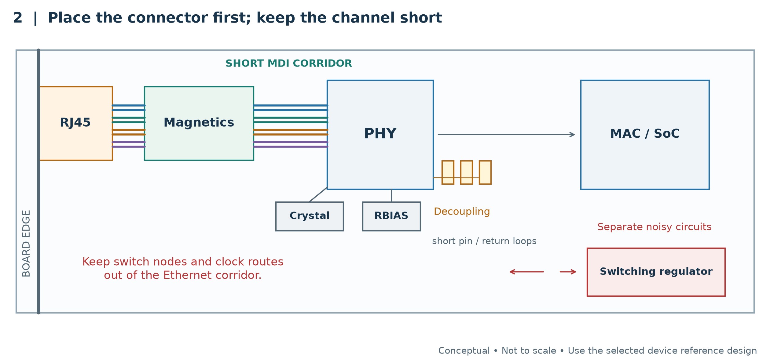
Figure 2. Placement floorplan that keeps the Ethernet channel short and separates it from switching noise.
Placement Order: RJ45, Magnetics, PHY, MAC
Place the RJ45 where the cable can enter without crossing the board. Put discrete magnetics immediately behind it, then place the PHY so the MDI pins face the magnetics. TI’s checklist recommends less than 2 in for each MDI route.[4] (Texas Instruments, Ethernet PHY PCB Design Layout Checklist) That is a vendor layout target, not a maximum Ethernet cable length or an IEEE channel limit. If the route needs a four-inch tour around another IC, placement is the problem; serpentine cannot repair it.
An integrated magjack reduces component count and removes the exposed cable-side route between magnetics and connector. Discrete magnetics provide more freedom to shape the isolation barrier and can simplify ESD separation. Neither option is automatically superior. Compare isolation rating, common-mode rejection, center-tap arrangement, PoE support, and the PHY vendor’s approved parts.
Turn the PHY so its crystal, RBIAS resistor, and local decoupling capacitors can sit against their pins. TI advises placing the oscillator and RBIAS component close to the PHY, with decoupling locations checked against the device datasheet. Keep switch nodes, inductors, fast clocks, motor phases, and high-current pulse paths away from both the PHY-side MDI traces and cable-side copper.
Stackup and Ground Planes for Ethernet
A four-layer Signal/GND/Power-or-GND/Signal stackup is a sound default because the top-layer MDI pairs can reference a nearby, continuous plane. TI and Microchip vendor guides recommend four layers for the device families they address, but this is design guidance rather than an IEEE requirement.[5] (Microchip Technology, Gigabit Ethernet Design Guide) A two-layer implementation may work when the PHY vendor permits it and impedance and EMC can be demonstrated, but the routing and return-current margin are smaller.
The plane beneath the MDI route must remain continuous except for intentional component keep-outs. A plane split forces displacement current to find a longer path, enlarging the loop and raising susceptibility and radiation. If a pair changes layers, keep the transition balanced and place nearby ground-return vias where the stackup permits. Minimize transitions rather than adding vias casually.
Set trace width and spacing from the actual finished stackup. Copper thickness, dielectric height, solder mask, and nearby grounded copper all affect the result. Record the stackup in EasyEDA and transfer the width and gap from a verified impedance calculator or field solver into its routing rules. A recorded stackup or clean DRC alone does not establish 100 Ω impedance. Do not “tune by eye” after the geometry has been calculated.
Ethernet Transformer Routing: MDI Differential Pairs
Ethernet transformer routing is the center of the layout. 1000BASE-T uses four signal pairs; 10BASE-T and 100BASE-TX use two. Each active pair needs controlled geometry, close P/N tracking, few discontinuities, and a continuous reference along the PHY-side route.
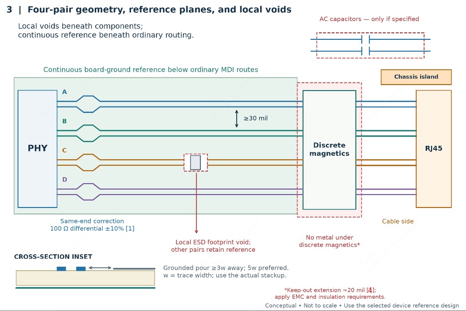
Figure 3. Four-pair MDI routing with controlled geometry, pair separation, and intentional component keep-outs.(one pair shown; apply to all active pairs)
Routing the Four Differential Pairs
Start with 100 Ω differential impedance and ±10% control, as recommended by TI, unless the cable or device documentation requires an adjusted value. Differential impedance is a property of the complete cross-section, not simply two narrow tracks placed near each other. Lock the stackup, calculate width and gap, and encode both into the design rules.
Route P and N together on one layer wherever possible. Keep bends symmetric, avoid stubs, and make both conductors see the same pads, vias, and reference environment. Every asymmetry creates a small difference in delay or impedance. Enough accumulated imbalance converts differential energy into common mode, which the cable can radiate efficiently.
TI recommends less than 2 in for each MDI route, at least 30 mil between different differential pairs, and as few vias and stubs as possible. The 30 mil rule separates one pair from another; it is not the gap between P and N. If same-layer grounded copper borders the route, hold it at least three trace widths away, with five widths preferred. That 3w/5w guidance applies to ground plane or pour and is intended to avoid added capacitive loading.
Length correction belongs at one end of the pair. Use compact, gently spaced tuning rather than a dense accordion with strong self-coupling. Applying compensation at both ends can leave two conductors equal in total length while exposing them to different local impedance and coupling histories. Route cleanly first, then add only the correction the pair needs.
Keep-Outs, Bob Smith Termination, and Earth-Ground Isolation
Keep metal out from under discrete magnetics on every layer. TI states this rule directly, while allowing metal under an RJ45 with integrated magnetics and describing a conditional exception when unavoidable metal is separated by a ground plane. For the other in-line components, TI recommends voids under magnetics, chokes, AC-coupling capacitors, and ESD diodes. In standard designs a two-layer void is recommended; automotive guidance recommends all-layer voiding, with two layers as the minimum. An extension of about 20 mil beyond the component is a starting point that must be adjusted to the EMC requirement.
Do not turn the keep-out into a slot beneath ordinary MDI routing. Preserve the appropriate reference on each side of local non-isolating components. Do not extend board ground across the transformer’s isolation barrier just to put copper beneath cable-side traces. Define the voids around exact packages, then inspect every plane layer rather than trusting a top-layer courtyard.
On the cable side, route the selected common-mode termination directly to the chassis island. Avoid long branches that add inductance. A 75 Ω network and high-voltage capacitor appear in vendor reference circuits, but the topology changes with PoE and magnetics construction. Copy the approved reference circuit for the chosen devices.
Keep chassis or earth ground separate from board ground by at least 20 mil on all layers according to TI’s checklist. TI’s recommended connection uses a capacitor and a resistor of at least 1 MΩ; implement the network shown in the approved system reference design. The capacitor value and voltage rating must come from the product’s safety, EMC, and reference-design requirements. This 20 mil PCB separation is not a certified safety creepage or clearance value: applicable insulation requirements can demand a larger barrier. Chassis ground is not necessarily protective earth, and a resistor across a required galvanic barrier may be unacceptable. A stitching via that shorts the domains defeats their intended separation.
Ethernet Length Matching Tolerance
The practical Ethernet length matching tolerance concerns P versus N inside each differential pair. TI’s checklist calls for matching within 20 mil for 1 Gb/s or 50 mil for 100 or 10 Mb/s; older TI guidance explicitly describes matching the two conductors within a pair. Treat those values as TI layout targets and check the selected PHY datasheet for device-specific limits.
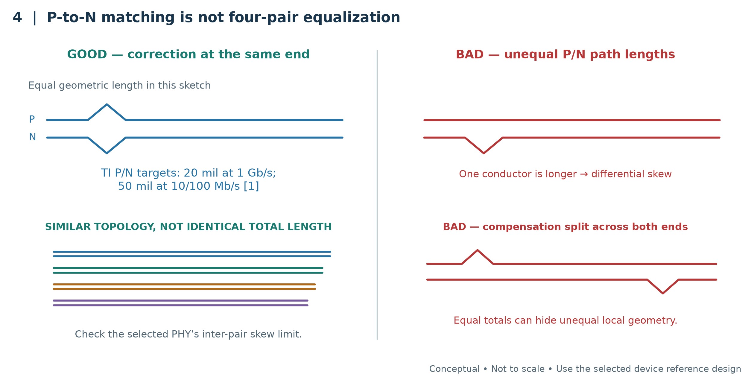
Figure 4. Length matching should correct imbalance within a pair without creating new discontinuities.
Mismatch matters because the two conductors no longer deliver opposite transitions at the same instant. If the one-way propagation velocity is vp and the physical mismatch is ΔL, the first-order skew is:
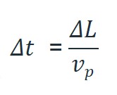
Here Δt is the arrival-time difference in seconds, ΔL is the magnitude of P-to-N length mismatch in metres, and vp is propagation velocity in metres per second for the actual PCB structure. This equation explains the direction of the effect; it does not replace a field solver or vendor limit. Effective permittivity and geometry determine vp.
The electrical result is differential-to-common-mode conversion. The receiver loses some of the rejection it expects from a balanced pair, while the common-mode component finds paths through parasitic capacitance, the magnetics, and the cable. That can reduce noise margin and make an EMC failure appear even when the differential eye still looks acceptable.
Do not force all four Gigabit pairs to match each other to 20 mil. That number is best applied within each P/N pair, not as a universal pair-to-pair rule. Pair-to-pair skew capability is PHY-specific. The LAN8831, for example, automatically corrects inter-pair skew; vendor board guides still publish finite PCB inter-pair limits.[6] (Microchip Technology, LAN8831 Gigabit Ethernet Transceiver Data Sheet) Keep the four paths topologically similar and verify the selected PHY’s pair-to-pair allowance instead of assuming deskew removes every PCB constraint.
Place any tuning at the same end of each pair, maintain enough spacing between adjacent serpentine segments, and avoid tuning simply to make the length report look tidy. The right review sequence is topology first, P/N mismatch second, impedance discontinuities third, and total route length last. Matching on the MAC-side digital bus is a different problem and is outside this article.
EMI, ESD, and Common Mistakes in Ethernet Routing
After impedance and pair balance, inspect return paths, protection placement, and nearby noise sources. Each can compromise an otherwise tidy channel.
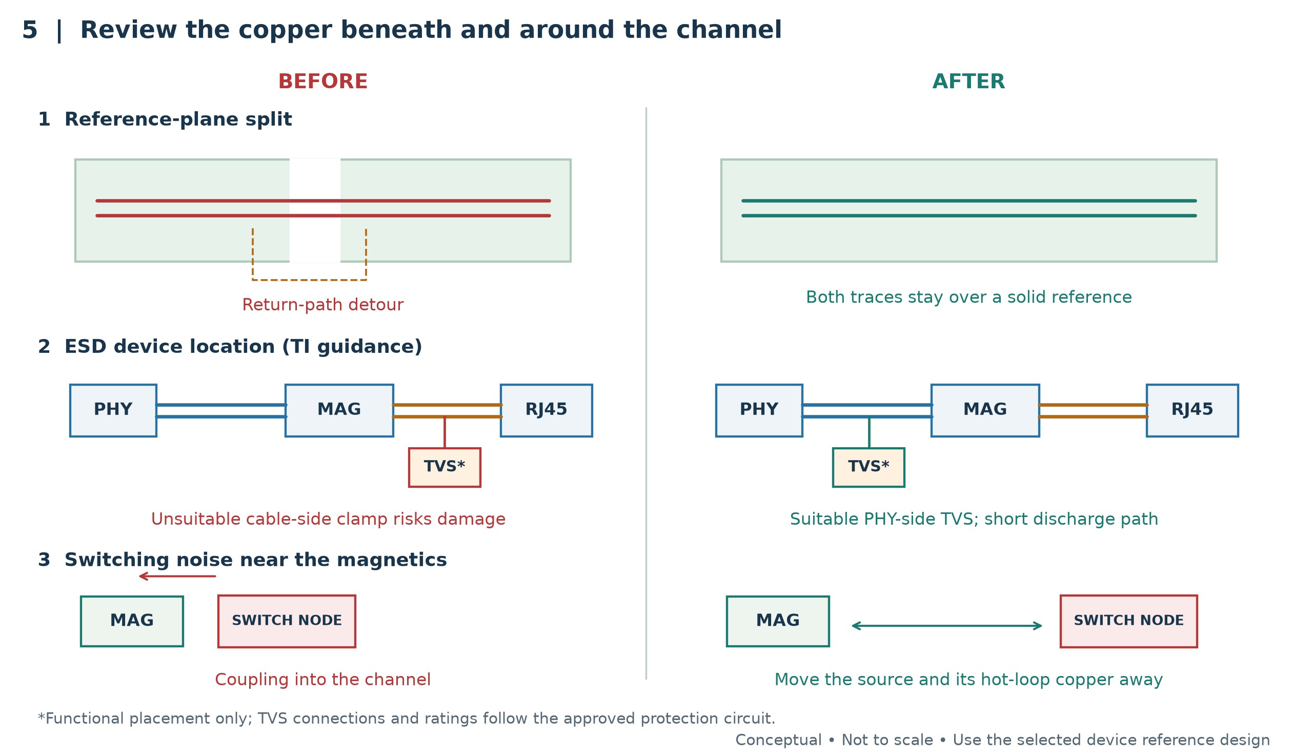
Figure 5. Correcting three common layouts removes avoidable return-path, protection, and coupling problems.
ESD Protection: Which Side of the Magnetics?
TI’s Ethernet-specific checklist recommends placing an ESD protection device on the PHY side of the magnetics, not the connector side. The reason is easy to miss: normal connector-side common-mode swings can be large enough to stress a protector chosen as though the line were a ground-referenced logic signal. A device in the wrong location may conduct or fail during a high but non-ESD event.
This is not permission to choose any low-capacitance diode and drop it beside the PHY. Confirm its working or acting-voltage range against the PHY datasheet and reference design. Place the device where the protected current path is short and where its required local plane void does not cut the reference beneath unrelated traces. Keep the discharge path away from crystal, reset, RBIAS, and supply-decoupling nodes.
System protection also depends on connector shield bonding, chassis geometry, enclosure construction, and the surge standard the product must pass. Layout guidance reduces risk; it does not certify immunity.
Common Ethernet Routing Mistakes
A pair crosses a plane split. Figure 5 shows two clean-looking tracks over a gap in the reference plane. Return current must detour around the gap, which enlarges the loop and raises EMI. Move the pair or restore a continuous reference.
Ground pour crowds the pair. A copper fill approaches one side of the route after impedance geometry was calculated without it. The extra capacitance shifts impedance and makes the two conductors see different surroundings. Pull grounded copper back by at least 3w, preferably 5w under TI’s guidance, then rerun the geometry check.
The MDI path wanders across the board. Long routes collect vias, layer changes, and opportunities for coupling. Move the PHY or magnetics until each route can meet the short, direct intent of the less-than-2-in TI recommendation.
Board ground leaks into the chassis island. A via, shield pad, mounting hole, or automatic plane fill silently joins the domains. Inspect every layer and net tie. Preserve the 20 mil all-layer separation and only the intentional capacitor/high-value resistor path.
Ethernet Routing Self-Check Checklist
Use this Ethernet PCB routing checklist before releasing fabrication files. Run it against every copper and plane layer, not just the top view.
| Check Item | What to Verify | Tool/Tip |
|---|---|---|
| Differential impedance | 100 Ω differential with ±10% control, unless device or cable data requires another target | Use the released stackup and field-solver geometry; verify the fabrication notes |
| Total MDI route | Each MDI route is under TI’s 2 in recommendation | Measure from PHY MDI pin through the applicable board route; do not count cable length |
| Intra-pair match | P to N is within 20 mil at 1 Gb/s or 50 mil at 10/100 Mb/s | Run pair-level length reports and inspect via/pad symmetry |
| Pair separation | Different MDI pairs remain at least 30 mil apart | Encode a pair-to-pair clearance rule, then inspect breakout exceptions |
| Grounded-pour clearance | Same-layer ground stays ≥3w away; 5w is preferred | Recheck impedance if copper fill changes after routing |
| Magnetics and component voids | No metal under discrete magnetics; intended voids exist beneath named in-line parts | Review all layers and extend generic voids about 20 mil where EMC needs permit |
| Chassis isolation | Board and chassis ground retain ≥20 mil separation on every layer | Check shield pads, mounting holes, pours, net ties, and the intentional RC connection |
| ESD and final DRC | Suitable protection is on the PHY side per TI; no open, width, spacing, or plane errors remain | Verify acting voltage against the PHY data and run EasyEDA DRC plus a manual reference-plane review |
FAQs About Ethernet PCB Routing
Q: What Impedance Should Ethernet Differential Pairs Be Routed At?
TI recommends 100 Ω differential impedance with ±10% control for the MDI traces. Use the actual stackup and confirm whether the selected PHY, magnetics, or cable documentation calls for an adjustment.
Q: How Long Can the Traces Between the PHY and the RJ45 Be?
TI recommends keeping each MDI route below 2 in and matching P to N within 20 mil for 1 Gb/s or 50 mil for 10/100 Mb/s. Those are PCB-layout recommendations, not Ethernet cable-length limits; the device datasheet remains authoritative for a particular design.
Q: Should There Be a Ground Plane Under the Ethernet Transformer?
For discrete magnetics, TI says no metal should be beneath the component on any layer, subject to its stated conditional exception. Keep a continuous reference beneath the routed MDI pairs, then apply the component-specific void at the magnetics footprint.
Q: Can I Route Gigabit Ethernet on a Two-Layer Board?
It is possible when the device vendor permits it and the board can hold impedance, reference continuity, and EMC performance. Four layers are strongly preferred in vendor guidance because a nearby solid plane makes those constraints easier to control. The Ethernet length matching tolerance does not compensate for a broken reference plane.
Conclusion About Ethernet PCB Routing
Reliable Ethernet PCB routing is decided by geometry and current paths: controlled differential impedance, close P/N tracking, short routes, deliberate keep-outs, and a clean boundary between board and chassis ground. None of those is rescued by a link LED. A marginal channel may negotiate on the bench and still fail during EMC testing or with a different cable.
Start with placement, route each pair over a continuous reference, and review the final planes after copper fills and mechanical features are complete. Apply TI’s numeric recommendations as vendor guidance, then check every value and topology against the actual PHY, magnetics, protection, connector, and PoE documentation.
For the MAC-to-PHY portion, see the companion article mentioned above. If you’d rather have JLCPCB’s engineers handle the layout, upload your schematic to our professional PCB layout services.
Sources
[1] Texas Instruments, “SimpliPHY Your Ethernet Design, Part 1: Ethernet PHY Basics and Selection Process,” SSZT321, March 2020. https://www.ti.com/lit/pdf/sszt321
[2] Microchip Technology, “Magnetics Guide,” ENT-AN0098, June 2018. https://ww1.microchip.com/downloads/en/Appnotes/VPPD-01740.pdf
[3] Texas Instruments, “AN-1469 PHYTER Design & Layout Guide,” SNLA079D. https://www.ti.com/lit/pdf/snla079
[4] Texas Instruments, “Ethernet PHY PCB Design Layout Checklist,” SNLA387, June 2021. https://www.ti.com/lit/an/snla387/snla387.pdf
[5] Microchip Technology, “Gigabit Ethernet Design Guide,” AN2054, 2016. https://ww1.microchip.com/downloads/aemDocuments/documents/OTH/ApplicationNotes/ApplicationNotes/00002054A.pdf
[6] Microchip Technology, “LAN8831 Gigabit Ethernet Transceiver with GMII/MII/RGMII Data Sheet,” DS00004725, §5.4. https://ww1.microchip.com/downloads/aemDocuments/documents/UNG/ProductDocuments/DataSheets/LAN8831-Data-Sheet-DS00004725.pdf
Keep Learning
HDMI PCB Layout Guidelines:Impedance & Length Matching
Key Takeaways Route the four TMDS pairs as 100 Ω differential pairs, and hold that value through vias, pads, and the connector. Match the P and N traces in each pair first, then match the pairs to each other within your silicon vendor's limits. Keep a solid reference plane under the whole route. Never cross a split. Put ESD protection as close to the connector as practical, so surge current is diverted early. Check the signaling type first. TMDS matching rules do not apply to HDMI 2.1 FRL. Introductio......
RGMII Routing Guidelines for Reliable Gigabit PCB Design
Key Takeaways RGMII is a 12-signal, single-ended, source-synchronous parallel interface; its TX and RX paths are separate timing groups. Match TXD[3:0] and TX_CTL to TXC. Match RXD[3:0] and RX_CTL to RXC. Do not match TX against RX. Budget the aggregate clock-to-data skew separately in each direction, and avoid unintentionally stacking a full PCB delay with an enabled silicon delay. Treat 50 Ω ±10%, 20 mil matching and a 6 inch route limit as TI layout guidance, not universal clauses of the RGMII spec......
Ethernet PCB Routing: Guidelines for MAC, PHY, and RJ45
Key Takeaways Route every MDI pair as a 100 Ω differential transmission line with ±10% control, unless the selected PHY or cable specification requires a different target. TI recommends keeping each MDI route below 2 in and matching P to N within 20 mil for 1 Gb/s or 50 mil for 10/100 Mb/s. Keep metal out from under discrete magnetics, separate chassis ground from board ground, and preserve a continuous reference beneath the routed pairs. TI’s Ethernet-specific guidance places suitable ESD protection ......
SFP Pinout Explained: PCB Layout & Design Guide
Key Takeaways The SFP pinout follows a standard 20-pin edge connector, with dedicated pins for power, ground, differential data pairs, and I2C control signals. The Tx and Rx differential pairs carry the high-speed optical or copper signal and need controlled 100 ohm differential impedance through the entire routing path. Low-speed control pins (TX_FAULT, TX_DISABLE, MOD_ABS, LOS, Rate Select/RS1) use standard single-ended routing and don't need impedance matching. Placing the SFP cage near the board e......
DDR5 PCB Layout Guidelines: Design Rules and Best Practices
Key Takeaways DDR5 raises the stakes on layout: 1.1V rails and data rates up to 8800 MT/s leave far less margin for error than DDR4 did. Target around 40–45 Ω single-ended for DQ/CA and 80 Ω differential for CLK/DQS — exact values come from vendor guidelines — and hold them through every via and connector. Keep DQ and DQS length matching within about 5 mil per byte lane, and never route a DDR5 signal over a gap in its reference plane. Plan for 8 to 12 layers with dedicated ground references next to ev......
Via Stitching in PCB Design: A Complete Guide
Key Takeaways Via stitching bonds same-net copper across layers with repeated plated vias, most often ground, to cut high-frequency impedance between regions. A grounded via next to a signal layer transition gives return current a short local path and helps confine the field around the via. Via fences along board edges and RF cavities suppress edge radiation, but their isolation is geometry- and frequency-dependent, with no universal dB value. Keep stitching pitch at or below one-twentieth of the in-b......