Guide to RF Circuit Design for High-Performance PCBs
15 min
- What Is RF Circuit Design?
- What Makes an RF PCB Work Reliably?
- Choosing PCB Materials for RF Circuit Design
- How PCB Manufacturing Shapes RF Circuit Performance
- FAQs About RF Circuit Design
- Conclusion
Key Takeaways
- Transmission Line Effect: Traces beyond one-tenth wavelength require a tight 50 ohm impedance to stop reflections.
- Continuous Return Path: Unbroken ground planes directly below traces prevent severe EMI.
- Strategic Laminates: Use FR-4 for basic 2.4 GHz, but upgrade to Rogers or PTFE for higher frequencies.
- Tight Fab Tolerances: Via inductances and dielectric variations alter impedance, requiring strict stackup specs.
RF circuit design begins where a PCB trace stops behaving like a wire. Above a few hundred megahertz, that copper has its own impedance, its own loss, and its own habit of radiating. It becomes a component you design, not a connection you simply draw. The cause is wavelength. A 2.4 GHz Wi-Fi signal repeats roughly every 70 mm along an FR-4 microstrip, so a few millimeters of feed already span a real fraction of a cycle. The voltage at one end no longer matches the voltage at the other.
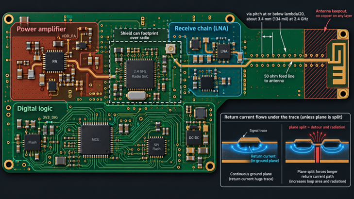
Figure 1: An RF PCB with a shielded radio, a 50 ohm feed line, and a via-fenced
Every width change, via or ground gap, then reflects part of the signal back toward its source. That is why two boards built from one schematic can perform very differently. This guide shows how RF circuits differ from conventional ones and what keeps an RF PCB predictable. It also covers when Rogers or PTFE laminate beats FR-4, and which fab tolerances decide whether the finished board matches your simulation.
What Is RF Circuit Design?
RF circuit design is the practice of building circuits that carry radio-frequency signals, from sub-gigahertz bands to millimeter-wave radar. The goal is for each signal to reach its load with a known impedance, low loss, and minimal leakage. On a PCB, the copper geometry and the laminate become working parts of that circuit.
How RF Circuits Differ From Conventional Circuits
A conventional circuit treats a trace as an ideal wire, because its signals change slowly compared with the board's travel time. That assumption fails once a trace passes about a tenth of a wavelength. At 2.4 GHz on FR-4 microstrip, the wavelength is about 69 mm (2.7 in). Any run beyond roughly 7 mm (275 mil) is therefore a transmission line.
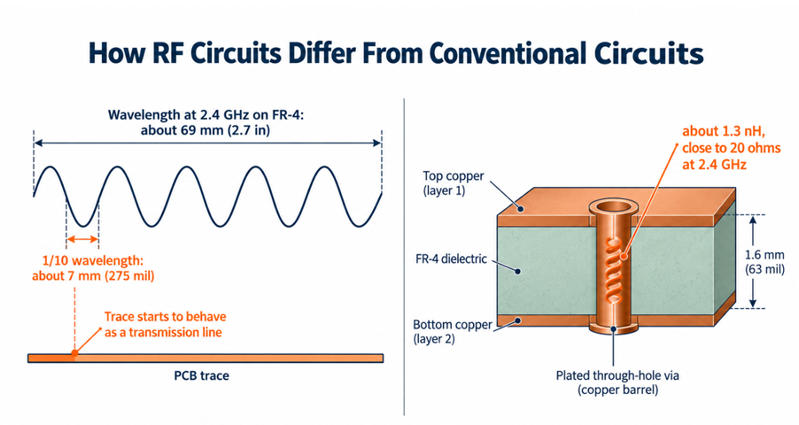
Figure 2: Trace length against wavelength at 2.4 GHz, with the hidden inductance of a via
Parasitics complete the picture, since every physical part carries inductance and capacitance that the schematic never shows. A 0.3 mm (12 mil) via through a 1.6 mm (63 mil) board adds about 1.3 nH. At 2.4 GHz, that is nearly 20 ohms in series with the signal, which is enough to detune a matching network on its own.
| Design Aspect | Conventional Circuit | RF Circuit | What It Changes on Your Board |
|---|---|---|---|
| Trace | Ideal wire | Transmission line with a fixed impedance | Width comes from the stackup, not the current |
| Ground | Shared 0 V node | Return half of every signal | Unbroken plane under every RF trace |
| Via | Free layer change | About 1 nH in series through 1.6 mm | Keep vias out of the RF path |
| Bypass capacitor | 100 nF covers it | Inductive above self-resonance | Add 10 to 100 pF at RF supply pins |
| Laminate | Mechanical carrier | Sets the circuit's loss and wavelength | Name the material on the fab drawing |
Key Requirements for RF Circuit Performance
- Impedance match, so power flows into the load instead of reflecting from it.
- Low loss, so the signal crosses the board with its noise floor intact.
- Isolation, so energy stays in the path it was meant for.
Impedance match is measured as return loss, which compares reflected power with incident power. Most RF systems standardize on 50 ohms and aim for a reflection (S11) below -10 dB, so under 10% of the power bounces back. Every discontinuity spends part of that budget, which means the board must hold 50 ohms before a matching network can help.
What Makes an RF PCB Work Reliably?
An RF PCB works reliably when each RF signal sees one impedance from source to load, with a clean return path directly beneath it. Both conditions are geometric, so the layout settles them before any board is built.
Controlled Impedance and Signal Paths
Controlled impedance fixes the trace width to the dielectric height and dielectric constant (Dk), so the line maintains 50 ohms end-to-end. Height dominates, so the stackup comes first. On a two-layer 1.6 mm (63 mil) FR-4 board, a 50 ohm microstrip is nearly 3 mm (118 mil) wide. That dwarfs the pads of a 0402 matching part.
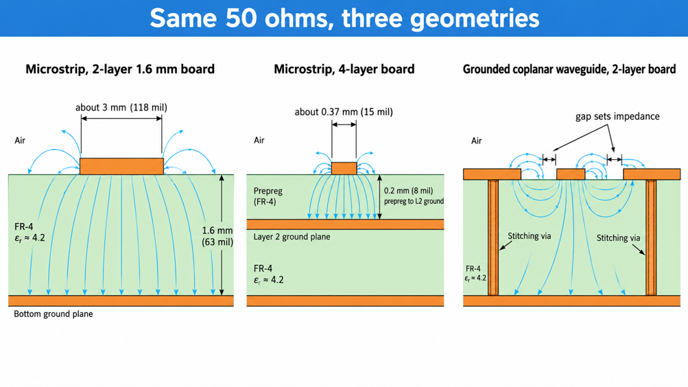
Figure 3: A 50 ohm microstrip on two and four layers beside a grounded coplanar waveguide
A thinner dielectric is the direct fix. A typical four-layer stackup places the ground plane about 0.2 mm (8 mil) below the top layer, so 50-ohm traces require only about 0.37 mm (15 mil) of clearance. On two layers, a grounded coplanar waveguide adds a ground plane alongside the trace. The side gaps then set the impedance instead of the board thickness.
Grounding, Return Paths, and Layout
Grounding on an RF PCB means a single continuous plane directly beneath every RF trace. On a four-layer board, layer 2 is kept solid across the RF section. On two layers, it is the whole bottom side, so routing signals there should be rare.
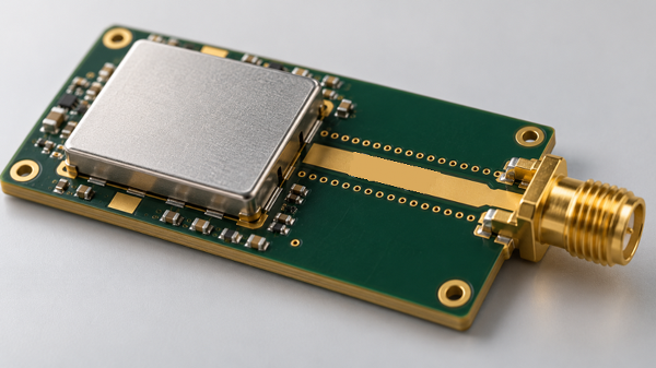
Figure 4: RF layout zoning with a solid ground, a via fence, and a shield can footprint
Return current at RF flows in the plane right beneath the trace. That path encloses the smallest loop, so it has the lowest inductance. The layout then separates circuits that must not hear each other. The power amplifier, the receive chain, and the digital logic each get their own zone, and the crystal stays away from the antenna feed. Four layout mistakes cut RF range most often:
- Routing RF across a plane split forces the return to go around the gap, so keep the plane continuous along the entire path.
- Leaving the top-layer unstitched creates islands that resonate, so stitch it at λ/20 or closer, about 3.4 mm (134 mil) at 2.4 GHz.
- Placing a bypass capacitor's ground via far from its pad adds inductance that cancels the capacitor, so put the via at the pad.
- Pouring copper near a module antenna detunes it, so keep the module's keepout clear. For an ESP32-WROOM-32E, Espressif cuts the base board away along the side beside the antenna, leaving at least 15 mm (591 mil) wide.
Choosing PCB Materials for RF Circuit Design
Laminate choice comes down to two numbers. Dk sets trace size and electrical length, while the dissipation factor (Df) sets how much signal turns into heat. FR-4 is loose on both, so the real question is how much looseness your design can tolerate.
When to Use Rogers PCB Materials
Rogers RO4000 laminates are glass-reinforced hydrocarbon ceramics, and their main value lies in their low loss. RO4350B has about a fifth of the Df of standard FR-4, at 10 GHz, which cuts dielectric loss from roughly 0.9 dB to 0.16 dB per inch (25.4 mm) of line.
Dk stability is the second reason, because filters, couplers, and antennas are cut to a fraction of a wavelength. RO4350B maintains its Dk within ±0.05, whereas FR-4 varies with glass style and resin content. Rogers also gives a design Dk of 3.66 for modeling, so a filter drawn at the 3.48 process value lands about 2% low. That is over 100 MHz at 5.8 GHz. Rogers earns its price on long lines above about 3 GHz and on power amplifiers that need better heat spreading.
PTFE PCB for High-Frequency Applications
PTFE laminates cut loss further, with Dk between about 2.1 and 3.0 and Df of roughly 0.001 to 0.002. Rogers makes PTFE too, as RT/duroid 5880 and RO3003 show, so "Rogers" names a supplier while "PTFE" names a chemistry. These boards appear in 24 GHz and 77 GHz radar, satellite links, and antenna arrays, where FR-4 loses several dB per inch.
The chemistry behind that low loss also makes PTFE hard to build. The material is soft and nonstick, so plating will not adhere to the wall of a drilled hole until the fab treats it with plasma or a sodium etch. PTFE carries that process work into every order, even where a fab prices it below RO4350B. Choose it for a loss budget, not by default. Below about 10 GHz, a hydrocarbon laminate typically provides most of the benefit while incurring fewer fabrication risks. The Rogers vs PTFE laminate comparison sets the two families side by side.
Balancing RF Performance and Manufacturability
The balanced choice is the cheapest laminate that still meets your loss and Dk budget. A 2.4 GHz Bluetooth or Wi-Fi board with a short feed works on FR-4 because the line loses a fraction of a decibel. That is why most 2.4 GHz modules use plain FR-4.
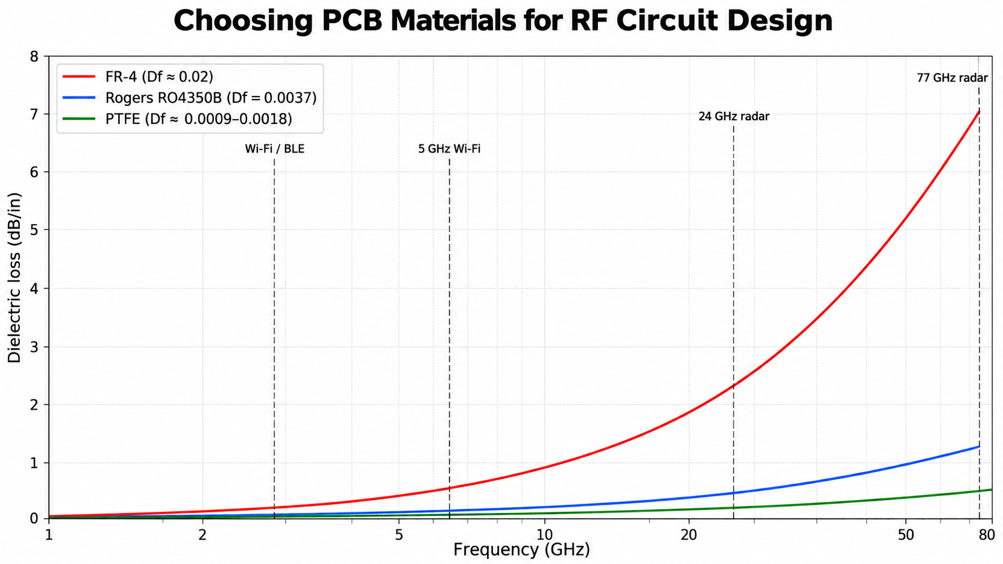
Figure 5: Dielectric loss versus frequency for FR-4, RO4350B, and PTFE
| Application | Typical Frequency | Suggested Laminate (Dk / Df) | Why It Fits |
|---|---|---|---|
| Bluetooth LE, 2.4 GHz Wi-Fi | 2.4 GHz | FR-4 (about 4.4 / 0.02) | Around 0.25 dB per inch, the lowest cost |
| GNSS and sub-6 GHz cellular | 0.6 to 6 GHz | FR-4, or RO4350B (3.48 / 0.0037) ahead of the LNA | Rogers only where loss adds to the noise figure |
| 5 GHz Wi-Fi filters, PA outputs | 5 to 7 GHz | RO4350B | Tight Dk keeps printed filters on frequency |
| 24 GHz radar, satellite receivers | 10 to 30 GHz | PTFE (2.2 to 2.65 / 0.0009 to 0.0019) | Lowest loss where every dB counts |
| 77 GHz automotive radar | 76 to 81 GHz | RO3003 ceramic-filled PTFE (3.00 / 0.0010) | FR-4 loss makes the band unusable |
For prototypes, JLCPCB's high-frequency PCB service builds two-layer boards on RO4350B or on ZYF-series PTFE (Dk 2.55 to about 3.0). RO4350B cores come in 0.51, 0.76, and 1.52 mm (20, 30, and 60 mil). Two layers are sufficient for an RF front end, since the circuit sits on one core over solid ground. Digital logic can move to a separate FR-4 board.
How PCB Manufacturing Shapes RF Circuit Performance
A simulation assumes perfect geometry, whereas the fab delivers geometry within a tolerance. RF performance depends on that gap, so the parameters worth controlling are those that most affect impedance and electrical length.
Maintaining Trace, Via, and Stackup Accuracy
Trace accuracy is set by etching, which removes copper laterally as well as downward, so traces come out narrower than drawn. A 0.025 mm (1 mil) error shifts a 1.1 mm (43 mil) line on 0.508 mm (20 mil) RO4350B by under 1 ohm. On a 0.37 mm (15 mil) FR-4 line, it costs about 2 ohms, because the error is a larger share of the width.
Via accuracy matters most under the RF chip. A radio IC's exposed pad serves as its main RF ground, tied to the plane via an array of vias. An open via can wick solder away from that joint during reflow. The voids add ground inductance where the amplifier needs least, so specify those vias as tented or filled.
Stackup accuracy comes down to dielectric height; the variable impedance follows most closely. A two-layer RF board uses one cured core with a published tolerance. On 0.508 mm (20 mil) RO4350B, that is about plus or minus 0.038 mm (1.5 mil). Multilayer prepreg flows during pressing, so choose your PCB thickness based on the fab's published stackup.
Controlling Impedance and Material Tolerances
Impedance tolerance is normally plus or minus 10%, so a 50 ohm line passes anywhere from 45 to 55 ohms. That band is the sum of smaller errors from separate process steps, and each one moves the line by a different amount.
| Source of Variation | Typical Spread | Effect on a 50 Ohm Microstrip | What to Specify |
|---|---|---|---|
| Etched trace width | ±0.025 mm (1 mil) | ±0.7 ohm on RO4350B, ±1.9 ohm on four-layer FR-4 | Wider traces on thicker cores |
| Dielectric height | ±7.5% on a core, about ±10% on prepreg | ±2.3 to ±3 ohm | The fab's published stackup |
| Dielectric constant | ±0.05 on RO4350B, 3.9 to 4.5 on FR-4 | ±0.3 ohm on Rogers, ±1.5 ohm on FR-4 | The laminate name on the drawing |
| Copper plating | 35 µm (1.4 mil) growing to about 60 µm (2.4 mil) | 0.6 to 1.1 ohm low | Finished copper in the model |
| ENIG finish | 3 to 6 µm (0.12 to 0.24 mil) of nickel | Extra loss at multi-GHz | Silver or OSP on long exposed lines |
A tolerance budget only helps if it reaches the fab. Put the target impedance, reference layer, and laminate name on the fabrication drawing. For multilayer boards, ask for impedance control on the RF layers so the fab can tune widths based on its measured data. JLCPCB does not yet offer it on two-layer boards, so size two-layer RO4350B lines from the core thickness and 3.66 design Dk.
Inspection and RF PCB Quality Control
Inspection for an RF board starts with the impedance coupon, a test strip etched beside your boards on the same panel. The fab measures it by time-domain reflectometry under IPC-TM-650 method 2.5.5.7. That confirms the combined result of width, height, and Dk, not each one separately. It cannot show how a filter performs, because a coupon only proves a straight line.
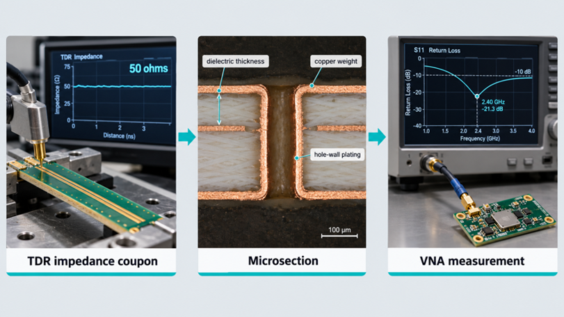
Figure 6: RF PCB quality control from TDR coupon and microsection to VNA measurement
Automated optical inspection, a camera that compares etched copper with the design data, catches width and gap errors. A microsection, a polished slice through the board, shows dielectric thickness, copper weight, and hole plating. The final verdict comes from a vector network analyzer (VNA) on the assembled board. S11 at the antenna feed shows the real return loss with parts, solder, and enclosure in place. If it misses -10 dB, the board can pass every fab check and still need retuning on the bench.
FAQs About RF Circuit Design
Q: Why do most RF circuits use 50 ohms?
50 ohms is a compromise inherited from coaxial cable. Air-filled coax loses the least near 77 ohms and handles the most power near 30 ohms. Cables, connectors, test gear, and RF chips settled on it, so parts connect without extra matching.
Q: Can I combine Rogers and FR-4 layers in one RF PCB?
Yes. A hybrid stackup places Rogers on the RF layer and FR-4 elsewhere, reducing costs for multilayer boards. The two expand differently with heat, so the fab must qualify the pairing. Without hybrids, a two-layer Rogers board, joined to the FR-4 main board via coax, provides the same split.
Q: Should I add a matching network footprint if the reference design has none?
Yes, because board thickness, ground clearance, and the enclosure shift antenna impedance. A pi footprint of one series and two shunt pads, fitted with a 0 ohm link and empty shunts, costs little. It lets you retune the match with a VNA after the first build.
Q: Is a higher dielectric constant ever better in RF circuit design?
Yes, when size matters more than loss. The wavelength on the board scales with the square root of Dk. A Dk near 10, therefore, makes filters and patch antennas about 40% smaller than a Dk near 3.5. The cost is narrower, more etch-sensitive traces.
Q: Should the solder mask be removed from RF traces?
Often, yes, above a few gigahertz. Solder mask has a much higher loss factor than RF laminate and reduces microstrip impedance by roughly 1-3 ohms. If it stays, include it in your impedance model so the simulation matches.
Conclusion
RF circuit design requires careful attention to PCB layout because the board itself directly affects signal performance. Copper trace geometry, grounding, and component placement influence impedance, signal loss, and interference between circuits. The choice of PCB material also matters, as its dielectric properties and manufacturing tolerances determine how closely the finished board matches the intended design.
For most 2.4 GHz applications, FR-4 remains a practical and cost-effective choice. With the growing adoption of 5G communication, automotive radar, and other high-frequency technologies, selecting the right PCB material and maintaining controlled impedance are becoming increasingly important. JLCPCB offers RF PCB manufacturing with FR-4 and specialized high-frequency materials, helping designers build reliable boards that meet their performance requirements.

Keep Learning
Guide to RF Circuit Design for High-Performance PCBs
Key Takeaways Transmission Line Effect: Traces beyond one-tenth wavelength require a tight 50 ohm impedance to stop reflections. Continuous Return Path: Unbroken ground planes directly below traces prevent severe EMI. Strategic Laminates: Use FR-4 for basic 2.4 GHz, but upgrade to Rogers or PTFE for higher frequencies. Tight Fab Tolerances: Via inductances and dielectric variations alter impedance, requiring strict stackup specs. RF circuit design begins where a PCB trace stops behaving like a wire. A......
PCB Basics: 50ohm PCB Trace with simple PI matching
When working with the RF (Radio Frequency) design, the transmission of signals between antennas and RF components on a PCB demands careful attention to detail. One critical aspect is the design of the antenna trace, which serves as the conduit for RF signals to propagate efficiently. In this article, we will delve into the significance of maintaining a 50 Ohm characteristic impedance for antenna traces in PCB design, along with best practices for achieving optimal performance in RF applications. Impor......
The Benefits of Coplanar Waveguide in High-Frequency PCB Design
Key Takeaways Coplanar waveguide (especially GCPW) improves high-frequency PCB performance by keeping the return path close and confining fields, which boosts signal integrity and reduces EMI/radiation. It also gives more impedance/layout flexibility (tuning both trace width and gap), but demands tighter manufacturing control of gap tolerances, copper roughness, and material Dk/Df—so field-solver impedance design and DFM checks are essential, with low-loss laminates preferred at higher GHz. Have you e......
6-Layer PCB Stackup and Buildup Guidelines
Printed Circuit Boards (PCBs) are the backbone of modern electronics, providing the necessary infrastructure for connecting and supporting various electronic components. As electronic devices become more complex and compact, the demand for multi-layer PCBs has increased. Among these, the 6-layer PCB is a popular choice for many applications. This article will delve into the specifics of 6-layer PCB stackup, its applications, optimal configurations, and guidelines for selecting the best manufacturer. W......
PCB Antenna Design: Types, Principles, and Best Practices
In the world surrounded with wireless communication, the demand for compact, inexpensive and reliable antennas has never been higher. Antennas are the application of electromagnetic waves. There are many theories and practicals available on antennas, but only few of them get recognised. For wireless data transfer the one solution can be usage of Printed Circuit Board (PCB) antennas. Using PCB antennas represents a convenient solution for integrating them directly into electronic devices, eliminating t......
Designing Antennas on PCB: A Beginner to Advance Guide
In today’s world of widespread wireless connectivity, the demand for small, affordable, and reliable antennas is higher than ever. Antennas act as real-world implementations of electromagnetic wave principles. They enable the sending and receiving of signals for a variety of wireless uses. While there is a lot of theoretical and experimental research in this area, only a few designs become widely used in actual products. Among the different options, Printed Circuit Board (PCB) antennas have become a p......