
The Benefits of Coplanar Waveguide in High-Frequency PCB Design
15 min
- What Coplanar Waveguide Is and Why It Matters
- Key Advantages for High-Frequency Applications
- Essential Design Techniques for Coplanar Waveguide
- Manufacturing Considerations for Reliable Coplanar Waveguide PCBs
- JLCPCB's Expertise in Coplanar Waveguide PCB Production
- FAQ about Coplanar Waveguide
Key Takeaways
Coplanar waveguide (especially GCPW) improves high-frequency PCB performance by keeping the return path close and confining fields, which boosts signal integrity and reduces EMI/radiation. It also gives more impedance/layout flexibility (tuning both trace width and gap), but demands tighter manufacturing control of gap tolerances, copper roughness, and material Dk/Df—so field-solver impedance design and DFM checks are essential, with low-loss laminates preferred at higher GHz.
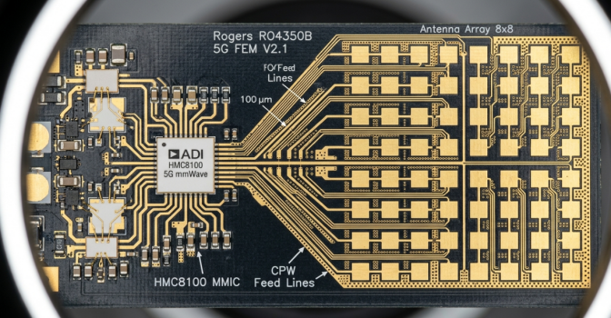
Have you ever thought about why there are RF and microwave PCB designs that route ground copper right next to the trace on the same layer? The latter method is known as a coplanar waveguide, and it has subtly become one of the most significant transmission line structures in high-frequency PCB design. Coplanar waveguides are ubiquitous in current electronics, in base stations operating 5G and automotive radar modules at 77 GHz. When you are designing boards with frequencies greater than 1 GHz, the transmission line geometry you select will have a direct influence on signal integrity, EMI performance, and manufacturing yield.
Microstrip and stripline have ruled the decades, but coplanar waveguide has had a distinct set of advantages, which have made it the favorite one in many high-frequency applications. This paper will discuss what a coplanar waveguide is, why it is important, the main benefits of using the method in high-frequency designs, the most important design methods, and what manufacturing considerations can guarantee good results. Be it an RF front-end module or a high-speed digital link, knowing coplanar waveguide will provide you with another potent weapon in your PCB design arsenal.
What Coplanar Waveguide Is and Why It Matters
Definition and Basic Working Principle
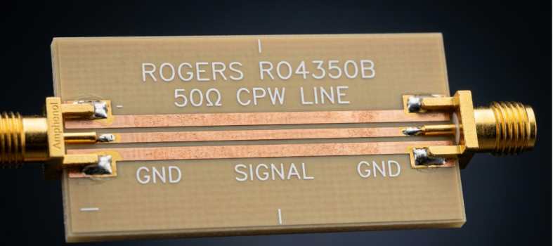
A coplanar waveguide (CPW) is a form of planar transmission line in which the ground and signal traces are both on the same PCB layer. The circuit is made up of a central conductor (the signal trace) and two ground planes on each side, with a small spacing between them. All three conductors lie on the dielectric substrate.
The signal trace is propagated by the electromagnetic wave, the electric field of which is concentrated mainly in the spaces between the signal trace and the adjacent ground planes. This is in stark contrast to a microstrip, where the current on the return is carried on an independent ground plane beneath the substrate. In a CPW, the return path is right on the same surface layer.
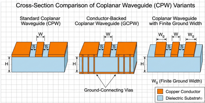
There are two main variants you will encounter in practice:
- Standard CPW (Ungrounded): The signal trace and coplanar ground planes are on the top surface, and there is no ground plane underneath. This is easier and is not used in actual PCBs.
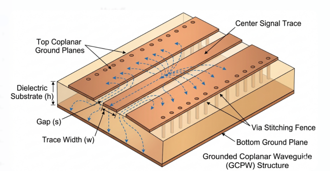
- Conductor-Backed CPW (CBCPW): This is similar to grounded coplanar waveguide (GCPW), except that a bottom-plane ground plane is included with the coplanar grounds joined together with vias. It is the most commonly used in production PCBs as it provides superior isolation and a stiffer return path.
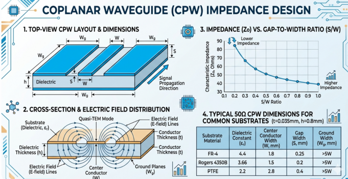
The characteristic impedance of a CPW is determined by the signal trace width (W), the separation between the trace and ground planes (G), substrate thickness (H), and dielectric constant (Dk) of the substrate material. The standard 50 ohm CPW on a standard FR4 (Dk = 4.4) could be implemented with a trace width of about 0.3 mm with a 0.15 mm gap between traces, but these values vary greatly with stackup.
When to Choose Coplanar Waveguide Over Other Transmission Lines
So, when does a coplanar waveguide make more sense than a traditional microstrip or stripline? Frequency, integration of components, and design flexibility are the answers. CPW is especially desirable at frequencies above 10 GHz, when microstrip performance starts to deteriorate because of surface wave radiation and increased dispersion. CPW is the default at millimeter-wave frequencies (30 GHz and higher) due to its better high-frequency properties.
Here is a quick comparison to help you decide:
| Parameter | Microstrip | Stripline | Coplanar Waveguide (GCPW) |
|---|---|---|---|
| Return Path Location | Below substrate | Above and below | Same layer + below (GCPW) |
| Frequency Range | DC to ~20 GHz | DC to ~30 GHz | DC to 100+ GHz |
| Component Mounting | Easy (surface) | Difficult (internal) | Easy (surface) |
| Via Requirements | Ground vias needed | Many ground vias | Fewer vias (ground is coplanar) |
| EMI Shielding | Moderate | Excellent | Very Good (GCPW) |
| Impedance Control | Trace width + substrate | Trace width + substrate | Trace width + gap + substrate |
| Typical Applications | General RF, WiFi | High isolation needs | mmWave, 5G, radar, MMIC |
Among the most significant practical benefits is that CPW enables you to place surface-mount components directly on the transmission line, without vias to a ground plane underlying. This is eliminated through inductance that may pose a significant problem at frequencies beyond 20 GHz. CPW is the intuitive and frequently the only viable option to use when the ground pads of MMIC (Monolithic Microwave Integrated Circuit) packages are on the same surface as the signal pads.
Key Advantages for High-Frequency Applications
Superior Signal Integrity and Reduced Loss
The signal integrity advantages of coplanar waveguide increase as frequency increases. Why not unravel? To begin with, CPW has less dispersion than microstrip at high frequencies. The electromagnetic field in a microstrip is a hybrid mode with an effective dielectric constant that varies with frequency and is a mixture of the field in the substrate and the field in air. CPW concentrates more of the field in the gaps between conductors, resulting in a more uniform propagation mode and less signal distortion across a wide bandwidth.
Second, the radiation loss is considerably minimized. Microstrip lines have a higher tendency to radiate energy at a higher frequency, particularly in discontinuities such as bends and junctions. A CPW structure has coplanar ground planes that provide natural shields to confine the electromagnetic field near the trace. Third, CPW design eliminates a significant source of parasitic inductance and impedance discontinuity because of the reduced via count. All vias in a high-frequency signal path contribute a minor bump in impedance. CPW reduces these discontinuities by ensuring that the ground return on the same layer as the signal is the same.
Better EMI Shielding and Compact Layout Flexibility
The signal trace is surrounded by coplanar ground planes, which form a natural electromagnetic shield. This is among the least realized advantages of CPW in thick, multi-function PCB designs.
The following are the main EMI and layout benefits:
- The coplanar grounds minimize crosstalk between adjacent transmission lines by offering instant electromagnetic confinement on the signal layer itself.
- In GCPW designs, the coplanar grounds and the bottom ground plane form a quasi-shielded environment that is like stripline, except that the component mounting ease of microstrip is available.
- Stitching of the CPW edges to the ground provides a useful via fence that additionally encapsulates the electromagnetic field.
- CPW allows impedance to be tuned by varying the trace and gap width, allowing designers greater flexibility in attaining desired impedance in narrow routing.
This is a particularly useful point. In microstrip, trace width is the only actual knob you have to control the impedance (using a fixed stackup). CPW has two independent variables: trace width and gap width. This implies that you can get 50 ohms with a smaller trace by having a smaller gap, which is an enormous benefit in compact layouts when routing is constrained.
Essential Design Techniques for Coplanar Waveguide
Impedance Calculation and Line Dimension Optimization
The basis of any coplanar waveguide design is to get the impedance correct. CPW characteristic impedance is a variable that is determined by four main variables:
- Signal trace width (W): Wider traces reduce the impedance.
- Gap width (G): Bigger gaps enhance the impedance.
- Substrate thickness (H): Thicker substrates raise the impedance a little.
- Dielectric constant (Dk): The greater Dk, the lower the impedance.
In the case of a typical (ungrounded) CPW, the impedance is expressed as a ratio of W / (W + 2G) and is a function of complete elliptic integrals. The simplified equation is:
Z0 = (30 pi) / (sqrt(Dk_eff) (K(k) / K'(k)))
In which K(k) represents the entire elliptic integral of the first kind, and K( k) is the complement. In reality, you will not compute this by hand, but instead use a field solver or an impedance calculator. In the case of GCPW (conductor-backed), the ground plane underneath also affects the impedance, and the calculation is more complex. More recent EDA systems, such as EasyEDA, Altium Designer, and KiCad themselves, have built-in impedance calculators or are compatible with field solvers such as Si9000, which can accurately compute GCPW geometries.
Here are some practical design rules for 50-ohm GCPW:
| Substrate | Dk | Trace Width (W) | Gap Width (G) | Substrate Height (H) |
|---|---|---|---|---|
| FR4 (standard) | 4.4 | 0.30 mm | 0.15 mm | 0.20 mm |
| Rogers RO4350B | 3.48 | 0.38 mm | 0.20 mm | 0.25 mm |
| Rogers RO4003C | 3.38 | 0.40 mm | 0.20 mm | 0.25 mm |
| PTFE (Teflon) | 2.2 | 0.50 mm | 0.25 mm | 0.25 mm |
Ground Plane Configuration and Via Placement Rules
The ground vias in a GCPW design are not just a nice-to-have. They play a crucial role in ensuring signal integrity and avoiding undesired parallel-plate waveguide modes between the coplanar ground and bottom ground plane.
These follow the placement rules of reliable GCPW designs:
- Place ground vias along both sides of the CPW signal trace at regular intervals.
- At your highest operating frequency, maintain via-to-via separation less than 1/20 lambda. In the case of a 10 GHz design on FR4, this would equate to a spacing of no more than 0.7 mm between vias.
- Install the first via row as near the gap edge as is permitted by your fabrication rules, usually 0.2 to 0.3 mm away.
- Staggered vias should be used in more than one row to form a more effective via fence at frequencies above 20 GHz.
- At transitions (bends, T-junctions, component pads), add via density to make up the discontinuity.
- Make sure that the minimum width of a coplanar ground plane on both sides of the signal trace is at least three times the width of the gap (3G minimum, 5G preferred).
The plane under the signal trace must be complete and continuous. Any slots, cutouts, or plane splits along a CPW trace will cause impedance discontinuities, and performance will be severely impaired. It is the same principle as microstrip, except that in CPW, it is more important since the return current is on the coplanar grounds and the bottom plane at the same time.
Manufacturing Considerations for Reliable Coplanar Waveguide PCBs
Precision Etching and Copper Profile Control
Compared to normal microstrip designs, coplanar waveguide PCBs require a higher manufacturing tolerance. This is because the impedance is very sensitive to the gap width, and gaps are usually far narrower than trace widths. A 0.15 mm pitch with a +/- 0.025 mm etching tolerance indicates that your gap may be within a range of 33, which is directly proportional to changes in impedance.
The manufacturing factors that are critical are:
Control of etch factor: The cross-sectional shape of chemical etching is trapezoidal, and thus, the gap at the top of the copper differs from the gap at the substrate surface. In the case of 1 oz (35 um) copper, the undercut of the etch can be 20 to 30 um on a side.
Copper roughness of surface: Above 5 GHz, the skin depth is on the order of the copper surface roughness. Rough copper enhances conductor loss. Standard FR4 copper foil has an Rz roughness of about 6 to 10 um, while low-profile foils (HVLP, VLP) bring this down to 2 to 3 um.
Minimum gap: Not every fabricator is capable of consistently making the tight gaps needed to support high-frequency CPW. The standard PCB processes can accommodate gaps as narrow as 0.1 mm (4 mil), although more sophisticated processes can accommodate 0.075 mm (3 mil) or smaller.
Material Selection and Tolerance Management
The substrate material has a massive impact on coplanar waveguide performance, especially at high frequencies. Here is what to consider when selecting materials:
| Property | FR4 (Standard) | FR4 (High-Speed) | Rogers RO4350B | Rogers RO4003C | PTFE (RT5880) |
|---|---|---|---|---|---|
| Dk (at 10 GHz) | 4.2 - 4.7 | 3.8 - 4.2 | 3.48 +/- 0.05 | 3.38 +/- 0.05 | 2.20 +/- 0.02 |
| Df (at 10 GHz) | 0.017 - 0.025 | 0.008 - 0.012 | 0.0037 | 0.0027 | 0.0009 |
| Dk Tolerance | +/- 10% | +/- 5% | +/- 1.5% | +/- 1.5% | +/- 1% |
| CTE (Z-axis, ppm/C) | 50 - 70 | 40 - 55 | 32 | 46 | 237 |
| Cost (Relative) | 1x | 2-3x | 5-8x | 5-8x | 10-15x |
In designs below 6 GHz, you can use standard or high-speed FR4 in place of GCPW, assuming that you consider the difference in Dk in your impedance analysis. The loss tangent of standard FR4 begins to significantly impair signal quality above 6 GHz, and you ought to switch to low-loss materials such as Rogers RO4000 series. Dk tolerance is especially significant in CPW since it has a direct impact on the accuracy of impedance. Even with ideal etching, Standard FR4 with +/- 10% Dk variation can exhibit impedance swings of 5% or greater. Rogers materials with tolerance of +/- 1.5% Dk tolerance offer far better impedance control, and this is the reason why most serious RF and mmWave applications are specified with Rogers material.
JLCPCB's Expertise in Coplanar Waveguide PCB Production
Advanced Fabrication Capabilities for High-Frequency Designs
The fabrication needs to extend beyond normal board production to produce reliable coplanar waveguide PCBs. JLCPCB provides the tools required to perform the high-frequency CPW designs, such as controlled impedance fabrication with a tolerance as fine as +/- 10%. Their features pertinent to CPW manufacturing are support of minimum trace and gap widths of 3.5 mil (0.09 mm), which encompasses most realistic GCPW geometries. Several high-frequency substrate materials exist, such as Rogers RO4350B, RO4003C, and other low-loss laminates that are critical in designs above 6 GHz.
Integrated DFM Support and Consistent High-Yield Results
Their Design for Manufacturability (DFM) review is one of the most important elements of coplanar waveguide designs that JLCPCB can offer. When you submit your Gerber files, their engineering department validates your CPW geometries to their manufacturing capabilities and identifies any possible problems before the manufacturing process starts.
This is particularly crucial to CPW since:
- Gap widths that are too small to be etched reliably are flagged early.
- Via placement around gap edges is verified to drill registration tolerances.
- The requirements of impedance control are compared with the material lots available.
The instant quoting system also allows you to instantly determine the cost impact of the various design options, including changing FR4 to Rogers or controlled impedance requirements. This fast-feedback mechanism allows you to work out the best design in terms of performance and cost before you make the decision to produce.
Scalable Solutions from Prototype to Volume Manufacturing
The designs of coplanar waveguides usually begin with prototypes requiring fast turnaround to be validated and tuned. The 1-2 day turnaround of JLCPCB to produce standard boards and lead times on advanced materials are competitive, so you can quickly iterate on your CPW designs.
CPW designs also go well with the SMT assembly service. Now that coplanar waveguide structures are uniquely made with easy surface-mount component integration, assembly, and fabrication by the same source, it guarantees that component placement accuracy is as good as your transmission line geometry. JLCPCB has made it cheap to prototype and refine your high-frequency coplanar waveguide designs, starting at only $2 to fabricate a PCB, and stencils as low as $6.
FAQ about Coplanar Waveguide
Q: What is the difference between a coplanar waveguide and a microstrip?
The main difference is the location of the ground return path. In a microstrip, the ground plane is on a separate layer below the substrate. In a coplanar waveguide, ground conductors are on the same layer as the signal trace, flanking it on both sides.
Q: What frequencies require a coplanar waveguide instead of a microstrip?
There is no hard cutoff, but CPW becomes increasingly advantageous above 10 GHz and is often the preferred or required choice above 30 GHz (millimeter-wave frequencies). Below 6 GHz, microstrip is usually simpler and works perfectly well.
Q: Can I use standard FR4 for coplanar waveguide designs?
Yes, for frequencies up to about 6 GHz, standard FR4 can work for GCPW designs. However, the higher Dk tolerance (+/- 10%) and higher loss tangent (Df 0.017-0.025) will limit impedance accuracy and increase signal loss compared to low-loss materials. For anything above 6 GHz, a low-loss laminate like Rogers RO4350B or RO4003C is strongly recommended.
Q: How do I calculate the impedance of a coplanar waveguide?
The impedance depends on trace width (W), gap width (G), substrate thickness (H), and dielectric constant (Dk). While closed-form equations using elliptic integrals exist, the most practical approach is to use a field solver or impedance calculator built into your EDA tool.
Q: What is the minimum gap width for coplanar waveguide PCBs?
Most standard PCB fabrication processes can reliably produce gaps down to 4 mil (0.1 mm). Advanced processes at facilities like JLCPCB can achieve 3.5 mil (0.09 mm) or finer. The minimum practical gap depends on your copper weight, as thicker copper requires wider gaps due to the etch undercut.
Keep Learning
Building Reliable High-Speed Performance with Effective Timing Analysis
Key Takeaways Timing analysis is essential for high-speed PCBs — clean signals can still fail if they miss setup or hold windows. Focus on setup time, hold time, clock skew, and propagation delay to ensure reliable data sampling. Prioritize length matching, controlled impedance, and proper stackup to maintain positive timing margins. Combine static timing analysis with dynamic simulation for best results. Precision manufacturing is critical — small variations in impedance or dielectric thickness can d......
Low Loss PCBs : Advanced Materials for Superior High-Speed Signal Performance
Key Takeaways Low Loss PCBs using advanced materials like Rogers RO4003C, RO4350B, and PTFE laminates deliver superior signal integrity by dramatically reducing dielectric loss at multi-gigahertz frequencies. Ideal for 5G, mmWave, RF, and high-speed digital designs, these boards offer significantly lower insertion loss, stable impedance, and better thermal performance compared to standard FR4. By choosing the right low-loss laminate and partnering with experienced manufacturers like JLCPCB, engineers ......
How to Reduce Insertion Loss for Better High-Speed PCB Performance
Key Takeaways Reducing insertion loss is essential for achieving reliable high-speed PCB performance. By selecting low-loss materials with lower Df, optimizing trace routing and stackup design, minimizing via transitions, using smoother copper foils, and applying precision manufacturing techniques, designers can significantly lower both dielectric and conductor losses. These strategies help maintain better signal integrity, wider eye openings, and higher data rates in multi-gigabit designs. Have you e......
How to Create the Perfect PCB Stackup for High-Speed and Reliable Designs
Key Takeaways A well-designed PCB stackup is the foundation of high-speed, reliable designs, determining signal integrity, controlled impedance, and EMI performance. Use symmetrical layers with adjacent reference planes, proper dielectric spacing, and copper balancing to avoid warpage and crosstalk. Choose standard FR4 for <3 GHz or low-loss materials (Megtron 6, Rogers) for higher speeds, and work closely with manufacturers for optimal results. Mastering your stackup is essential for high-speed succe......
Achieving Reliable High-Speed Performance with PCB Transmission Lines
Key Takeaways PCB Transmission Lines are essential for reliable high-speed PCB performance in USB 3.0, PCIe, DDR4, and RF designs, turning traces into controlled-impedance structures that eliminate reflections, crosstalk, and attenuation. Select microstrip, stripline, or GCPW geometries with accurate calculations, continuous reference planes, mitered bends, and 3W spacing, then rely on precise etching, copper profile control, and TDR testing at JLCPCB for consistent results from prototype to volume pr......
Backdrill Vias: Enhancing Signal Integrity in High-Speed PCBs
Key Takeaways Backdrill vias remove unused copper stubs from plated through-hole vias, shortening the residual stub to under 0.15 mm (6 mils). This eliminates impedance discontinuities, reflections, and resonances in high-speed signals above 5–10 Gbps. It delivers better return loss, insertion loss, lower jitter, and clearer eye diagrams — all while keeping simple stack-ups and far lower cost than blind/buried vias. Use backdrilling for any stub longer than 15 mils (0.381 mm), especially on boards thi......