Effective Escape Routing Strategies for High-Density BGA Success
14 min
- What Escape Routing Is and Why It Matters:
- Key Factors That Determine Escape Routing Success:
- Proven Escape Routing Techniques and Best Practices
- Design Trade-offs and Common Pitfalls
- Manufacturing Considerations for Escape Routed Designs
- JLCPCB's Expertise in High-Density Escape Routing
- FAQ about Escape Routing
- Conclusion
Key Takeaways
- Escape routing is essential for successfully fanning out high-density BGAs, especially at 0.5 mm pitch and below.
- Use dogbone fanout for ≥0.5 mm; switch to via-in-pad (filled & capped) for finer pitches.
- HDI microvias and stacked vias significantly improve routing density and reduce layer count.
- Maintain symmetry and short stubs for differential pairs to preserve signal integrity.
- Combine smart stackup, DFM checks, and capable fabrication for reliable, high-yield results.
Ever put a 484-ball BGA on your board and hit "route," and watch your EDA tool choke? You are not alone. When hundreds of pins are in a grid, and you can't seem to find an easy way out, that's when escape routing is in effect. The art of routing signals from beneath a dense component out to the rest of the board is called escape routing. With the increase of pin counts and package pitches down to 1/2mm and less, this becomes the largest single constraint in contemporary layout.
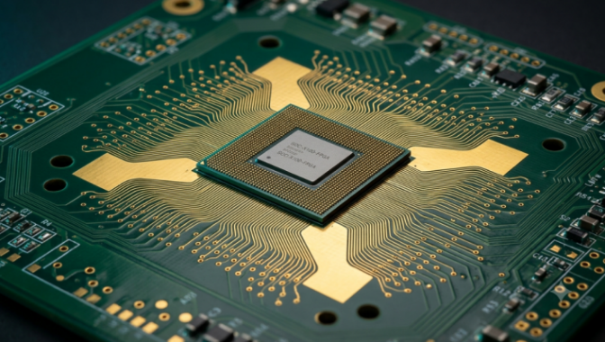
If you get it right, your board is manufacturable, reliable, and clean. If you're not, you'll be subject to reflections, shorts, and painful yield losses. Throughout this tutorial, we'll discuss the basics of what PCB escape routing actually entails, the parameters that determine the outcome, the most effective way to route the fans out by pitch, the compromises to consider, and the manufacturing capabilities that make it possible. Let's dig in.
What Escape Routing Is and Why It Matters:
Definition of Escape Routing in Modern PCB Layout
But what is escape routing? As simply stated, it's the process of bringing a short PCB trace from each pad of a dense component out to where normal routing can proceed. Consider it similar to leading individuals out of an overcrowded stadium via the closest exit before they are able to wander down the street. With BGAs (Ball Grid Arrays), the pads are laid out in a 2D grid beneath the package. You can't just go over the top layer since the inner balls are all around.
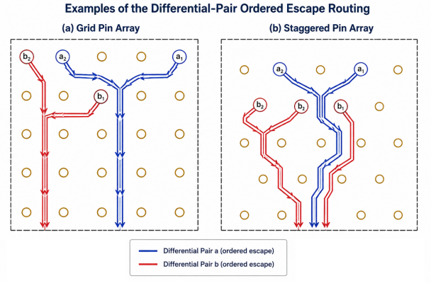
Escape routing addresses this by spreading out each pad to a via or channel on each layer until all signals can be routed. This is different from regular routing. Escape routing only applies to the one hot escape out of the component footprint. When the signals reach the edge of the array and enter the “escape lane” or fall to an inner layer, the rest of the layout is conventional.
Challenges Posed by Fine-Pitch BGAs and High Pin Counts
Difficulty increases rapidly as the geometry decreases. A 1.0 mm pitch BGA allows you to place a via between the balls and also route a trace through the gap. Change to 0.4 mm pitch, and that gap is pretty much gone. The core issue is numbers. There may be only about 0.4 mm clearance between two adjacent 0.8 mm pitch pads to accommodate a via pad, a trace, and the necessary clearance on both sides.
A standard through-hole via just won't fit at 0.5 mm or lower, meaning you must go with microvia and high-density interconnect (HDI) construction. This is aggravated by the fact of having a large number of pin counts. Four or more signal layers may be required for a 1,000-ball device to exit all nets, and the cost and complexity increase with each additional layer. The crux of the matter is the balance between routability and the number of layers that each designer must deal with.
Key Factors That Determine Escape Routing Success:
BGA Pitch, Via Technology, and Layer Stackup Influence.
There are 3 main escape routing variables that determine the success or failure of any escape routing attempt.
The first is pitch: It is the distance between the middle of two balls. Pitch determines the actual budget for all else.
Second is via technology: A standard mechanical via (0.2 mm minimum drill at JLCPCB) is able to reach a minimum of 0.8 mm pitch. Laser-drilled microvia (0.15 mm minimum) and via-in-pad are required to get the board space back.
Third is stacks of layers: The more layers of signal, the fewer balls escaping per layer, reducing congestion but increasing costs. A good stackup makes sure that ground planes and power planes are used in a manner where they are next to each other, so that when a signal moves from one layer to another, they will have a nice, clean return path.
Impact on Signal Integrity, Power Integrity, and Routability
Escape routing isn't only a geometry puzzle. Each via-stub, layer transition, and impedance discontinuity that you introduce at fanout impacts signal integrity. If long via stubs are used on high-speed nets, reflections and resonances will occur that will affect the eye diagram.
Power integrity is just as important. Power and ground balls should come out with as little inductance as possible (via dropping directly to planes or wide traces). Poor power fanout starves the device when switching fast and contributes noise to the PDN. The escape pattern can be dense, meaning that 1 escape can block 3 others, and the order and symmetry of your fanout are what will directly determine whether or not you can route the full package.
Proven Escape Routing Techniques and Best Practices
Dogbone, Via-in-Pad, and Advanced Fanout Patterns
The classic workhorse is the dogbone (or dog-bone) pattern. Each BGA pad is connected to a via located in the space between four balls in a pattern that resembles a dog's bone. It is inexpensive, easy to understand,d and is reliable up to 1.27 mm pitch, as low as 0.5 mm pitch.
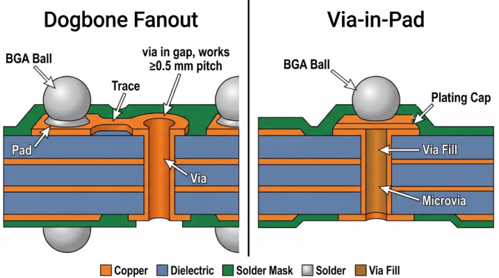
With via-in-pad, a via is positioned right inside the BGA pad. This is needed to release a lot of space, and below 0.5 mm pitch, it becomes critical that the via be filled with epoxy and capped with plating so that no solder will wick into the barrel during reflow. Fine-pitch BGAs require via-in-pad with resin fill & cap plating, and JLCPCB does it. In the highest densities, advanced HDI fanout can be used to create routing on multiple thin layers, using either stacked or staggered microvia technology with buried vias. This is the way a thousand-plus balls escaped in a 0.4mm pitch device without the use of a 20-layer board.
Routing Optimization for Different Pitch Sizes and Densities
There are various playbooks for different pitches. The table below shows an overview of known starting points for each common pitch.
| BGA Pitch | Recommended Fanout | Via Type | Typical Trace/Space | Layer Impact |
|---|---|---|---|---|
| 1.0 mm | Dogbone | Mechanical through-hole | 4-5 mil | Low, 2-4 layers |
| 0.8 mm | Dogbone | Mechanical or microvia | 3.5-4 mil | Moderate, 4-6 layers |
| 0.65 mm | Dogbone + ordered routing | Microvia preferred | 3.5 mil | Moderate to high |
| 0.5 mm | Dogbone or via-in-pad | Microvia | 3-3.5 mil | High, HDI likely |
| 0.4 mm | Via-in-pad only | Stacked/staggered microvia | 2.5-3 mil | Very high, HDI required |
One easy rule of thumb to keep in mind is that the outermost row(s) of a BGA can very often be routed on the top layer with no via whatsoever, hence designers often place easy-to-route or non-critical signals in these outermost rows. Try to avoid using inner-row vias except for the nets that require a layer change.
Managing Differential Pairs and High-Speed Signals in Escape Areas
Special care must be taken with high-speed interfaces in the escape zone. If using differential pairs such as PCIe, USB 3.x, or SerDes lanes, ensure that both sides of the pair are treated symmetrically with the fanout, seeing the same via structure and trace length.
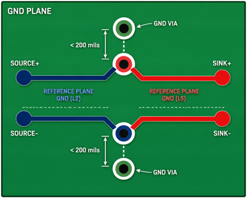
Practice these tips for a fast escape:
- Consider routing both legs of a differential pair through adjacent and symmetric vias to maintain coupling.
- Skew intra-pair length as close as possible at fanout and adjust the remaining skew after the escape zone.
- Place return-path vias (ground stitching vias) near signal vias to provide a low-impedance path for the return current.
- Hit the right differential impedance (85 ohms for PCIe/USB and 90-100 ohms for other standards).
- Keep via stub length short by escaping on high-speed nets to top layers, or back-drilling on thick stackups.
The length of the escape is not the most important thing; the most important thing is that it is an escape symmetric. The common-mode noise and uncorrectable skew downstream is a tiny asymmetry in the fanout.
Design Trade-offs and Common Pitfalls
Balancing Escape Routing with Thermal, Mechanical, and Cost Constraints
A route of escape is never an independent act. Thermal vias and signal vias should be planned at the same time; via-in-pad, for example, is good for routability, but can interfere with the thermal pad of a power device. For successful fine-pitch assembly, filled and capped vias are necessary, but costly. The largest cost lever is layer count. Adopting techniques such as ordered routing and outer-row escapes first can help avoid the added expense of bringing additional layers to a circuit: going from a 6-layer HDI stackup to a 10-layer stackup could double the cost of circuit fabrication. In addition, dense microvia arrays have more stringent mechanical requirements since both registration and material must be chosen carefully for thermal cycling.
Typical Mistakes That Lead to Poor Yield or Signal Issues
When it comes to escape routes, there are some simple mistakes that lead to many escape route failures:
- Utilizing via-in-pad with no solder in the hole, allowing solder wicking from the hole and leaving an open or starved joint.
- Sizing smaller than the capability of the fabricator, causing shorts and etch defects.
- Ignoring return paths, so high-speed signals radiate and pick up crosstalk in the fanout.
- Skew induced by the asymmetric placement of vias on a differential pair.
- Failure to consider the aspect ratio on microvias, thus impacting plating reliability.
Almost all of these will be revealed in a manufacturer's DFM report. It is much more cost-effective to detect them before fabrication as opposed to a failed reflow batch.
Manufacturing Considerations for Escape Routed Designs
DFM Requirements for Fine Features and High-Density Boards
DFM (Design for Manufacturing) is the meeting of an elegant escape pattern with physical reality. Hard limits on fanout are imposed by the fabricator's minimum trace width, spacing, via size, and annular ring. On high-density boards, these parameters must be confirmed early in the board: minimum PCB trace width and space; minimum microvia and mechanical via diameter; via-in-pad fill capability; and the layer-to-layer registration tolerance. Designing to actual ability from initial placement saves on expensive re-spins.
Process Capabilities Needed for Reliable Production
The following process capabilities are essential for reliable fine-pitch production to be achieved:
- Microvia down to 0.15 mm with 0.4 - 0.5 mm pitch escapes with laser drilling technology.
- So via-in-pad structures are formed via filling and cap plating, which can realize BGA ball mounting without solder loss.
- Controlled impedance fabrication of differential and single-ended targets holding through escape.
- Sequential lamination of buried and stacked microvia HDI stackups.
- Automated optical inspection (AOI) and electrical test for short/open detection in dense areas.
Even the best layout will not cause yield without these. The best way to a working board is to match your design to a fabricator that provides all of them.
JLCPCB's Expertise in High-Density Escape Routing
Advanced DFM Analysis Specialized for BGA Fanout Challenges

Whether it is a trace width smaller than the capability or insufficient clearance for vias, JLCPCB's instant DFM analysis points out exactly where the problems lie. This check is performed on your Gerbers prior to order, thus taking a risky fine-pitch layout and making it a verified design for manufacture. The feedback is instantaneous, so you can try a challenging 0.5 mm pitch fanout in minutes, instead of waiting days for a manual review. This high-speed loop really helps when tuning a dense BGA breakout.
Precision Fabrication Supporting Complex High-Density Layouts
As far as the fabrication aspects are concerned, JLCPCB can handle the small geometry required for fine-pitch BGAs, such as 3.5 mil traces and space, 0.15 mm laser-drilled microvia, 0.2 mm mechanical via, and via-in-pad with epoxy fill and cap plating. These are the very attributes that make 0.4 mm and 0.5 mm pitch escapes possible. If you are being driven to an unnecessarily thick board due to a high pin count device, HDI stackups with buried and stacked microvias are available for the densest of designs.
The same process is followed from prototype (2 days) to full production; the board you validate is the board you scale. Even as your escape patterns become more HDI, controlled impedance, AOI, and electrical testing ensure high yield. For those looking to implement these principles, JLCPCB's DFM check and HDI capability will make dense BGA fanout accessible from prototype to volume.
FAQ about Escape Routing
Q: What is escape routing in PCB design?
Escape routing is the process of routing a short trace from each pad of a dense component, usually a BGA, out to a via or open channel where normal routing can continue. It is the critical first step in breaking signals out from underneath a packed grid of pins.
Q: When should I use via-in-pad instead of dogbone fanout?
Use dogbone fanout for pitches of 0.5 mm and above, where a via fits in the gap between balls. Switch to via-in-pad at pitches below 0.5 mm, and always fill and cap those vias to prevent solder wicking during reflow.
Q: What trace width and spacing do fine-pitch BGAs need?
A 0.8 mm pitch BGA typically routes with 3.5-4 mil trace and space, while 0.4 mm pitch HDI designs may need 2.5-3 mil features. Always confirm the numbers against your fabricator's capability, such as JLCPCB's 3.5 mil minimum.
Q:How many layers does a high pin-count BGA require? 1
It depends on pitch and pin count, but a rough guide is that only a couple of ball rows escape per signal layer. A 1,000-ball fine-pitch device often needs four or more signal layers, frequently in an HDI stackup.
Q: How do I keep high-speed differential pairs clean through the escape zone?
Route both legs through adjacent, mirrored vias, match their lengths tightly, and place ground return vias nearby for a low-impedance return path. Symmetry through the fanout matters more than absolute trace length.
Conclusion
High-density design works or doesn't work with escape routing. It's the small door every signal has to go through, and the decisions made here affect signal integrity, power delivery, manufacturing yield, and cost. With even a thousand-ball BGA, if you master the pitch-based playbook, match dogbone to the right geometry, and keep your differential pairs symmetric, then you can route it.
Pin counts continue to increase, while packages continue to get smaller, HDI and microvia packages are becoming commonplace. Today's designers who know about the PCB escape routing will be the ones who ship tomorrow's boards with higher speed and higher density without any surprises. So when it's time to build, the best way to get from schematic to a reliable, high-yield product is to pair it with a fanout as well planned as a fabricator like JLCPCB, which knows how to handle the challenges of the fanout thanks to their DFM analysis and HDI process.

Keep Learning
PCB Basics: 50ohm PCB Trace with simple PI matching
When working with the RF (Radio Frequency) design, the transmission of signals between antennas and RF components on a PCB demands careful attention to detail. One critical aspect is the design of the antenna trace, which serves as the conduit for RF signals to propagate efficiently. In this article, we will delve into the significance of maintaining a 50 Ohm characteristic impedance for antenna traces in PCB design, along with best practices for achieving optimal performance in RF applications. Impor......
The Benefits of Coplanar Waveguide in High-Frequency PCB Design
Key Takeaways Coplanar waveguide (especially GCPW) improves high-frequency PCB performance by keeping the return path close and confining fields, which boosts signal integrity and reduces EMI/radiation. It also gives more impedance/layout flexibility (tuning both trace width and gap), but demands tighter manufacturing control of gap tolerances, copper roughness, and material Dk/Df—so field-solver impedance design and DFM checks are essential, with low-loss laminates preferred at higher GHz. Have you e......
6-Layer PCB Stackup and Buildup Guidelines
Printed Circuit Boards (PCBs) are the backbone of modern electronics, providing the necessary infrastructure for connecting and supporting various electronic components. As electronic devices become more complex and compact, the demand for multi-layer PCBs has increased. Among these, the 6-layer PCB is a popular choice for many applications. This article will delve into the specifics of 6-layer PCB stackup, its applications, optimal configurations, and guidelines for selecting the best manufacturer. W......
PCB Antenna Design: Types, Principles, and Best Practices
In the world surrounded with wireless communication, the demand for compact, inexpensive and reliable antennas has never been higher. Antennas are the application of electromagnetic waves. There are many theories and practicals available on antennas, but only few of them get recognised. For wireless data transfer the one solution can be usage of Printed Circuit Board (PCB) antennas. Using PCB antennas represents a convenient solution for integrating them directly into electronic devices, eliminating t......
Designing Antennas on PCB: A Beginner to Advance Guide
In today’s world of widespread wireless connectivity, the demand for small, affordable, and reliable antennas is higher than ever. Antennas act as real-world implementations of electromagnetic wave principles. They enable the sending and receiving of signals for a variety of wireless uses. While there is a lot of theoretical and experimental research in this area, only a few designs become widely used in actual products. Among the different options, Printed Circuit Board (PCB) antennas have become a p......
Backplane Basics: What it is and Why it Matters in High-Speed Electronics
Key Takeaways System Backbone: Backplanes act as passive interconnect boards, routing high-speed data and power across sub-cards without hosting central CPUs. Solderless Press-Fit: They use press-fit connectors to reliably hold thousands of pins while preventing thermal distortion on thick boards. Thick Multilayer Design: Built with 2.0–3.2 mm board thickness, 6–32 layers, and strict ±0.05 mm PTH hole tolerances for superior rigidity. Backdrilling for SI: Controlled-depth backdrilling removes unused v......