How SMA Connectors Work in RF PCB Design
14 min
- What Is an SMA Connector?
- How SMA Connectors Work With RF PCBs
- SMA Connector PCB Layout Considerations
- Manufacturing RF PCBs for Reliable SMA Connections
- Common SMA Connector Applications
- FAQs About SMA Connectors
- Conclusion
Key Takeaways
- Focus on the Launch: Signal loss happens where coax turns into a flat trace, not inside the SMA body.
- Clear Ground Under Pads: Cut ground planes under launch pads to control capacitance and keep 50 ohms.
- Place Ground Vias Close: Put ground vias next to connector legs to shorten return paths.
- Account for Tolerances: Trace etching and board thickness directly alter launch impedance.
- Handle with Care: Use a torque wrench on joints and switch to high-frequency boards above 6 GHz.
An SMA connector is a threaded 50 ohm coaxial connector, and its body is rarely the weak point on an RF PCB. The few millimeters where the center pin lands on your board usually decide the result. Inside the connector, the signal travels as a field wrapped evenly around the center pin. On the board, that field has to fold down into a flat trace over a ground plane. Every change of shape is a change of impedance, so part of the signal reflects.
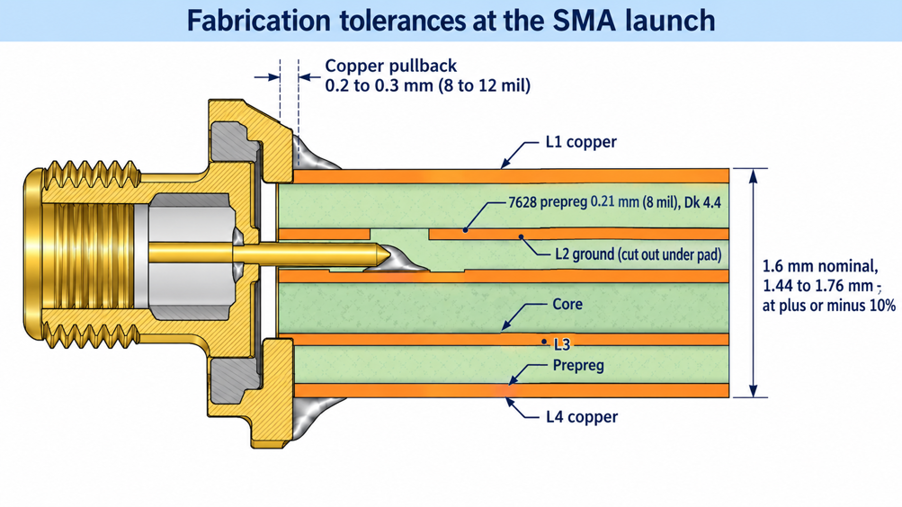
Figure 1: An edge-launch SMA connector on an RF PCB
The pad under the pin is wider than the trace, so it acts as a small capacitor. A 100 MHz signal ignores it, but a 6 GHz signal does not. This guide explains how an SMA connector is built and what it does in an RF system. It then covers launch design, ground vias, footprints, fabrication tolerances, and the applications where SMA connectors earn their place.
What Is an SMA Connector?
An SMA connector (SubMiniature version A) is a threaded coaxial connector that maintains 50-ohm impedance from DC to about 18 GHz. It joins a coaxial cable to a PCB, an instrument, or another cable. Because the screw coupling maintains the contact pressure, the joint is repeatable every time you make it.
SMA Connector Structure and Interface
Every SMA connector has four parts: a center contact, a PTFE dielectric, a metal outer body, and a threaded coupling. The plug, or male half, carries a solid pin and a threaded nut. The jack, or female half, carries a slotted socket and an external thread. The jack is normally the half soldered to a PCB, because the rotating nut belongs on the cable.
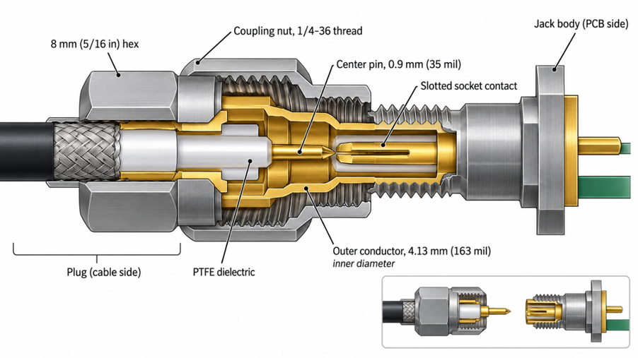
Figure 2: Cutaway of a mated SMA plug and jack
The internal geometry fixes the impedance. IEC 61169-15 defines the SMA interface around an outer conductor with a 4.13 mm (163 mil) inner diameter, filled with PTFE. The ratio of the conductor diameters and the dielectric constant of PTFE set the 50 ohms. So a dent, a gap, or a bent pin changes the impedance at exactly that spot.
| Parameter | Typical Value | What It Means for Your Design |
|---|---|---|
| Impedance | 50 ohms | Trace, pad, and launch must hold 50 ohms, too |
| Frequency range | DC to 18 GHz; precision parts to 26.5 GHz | The board launch usually runs out of margin first |
| Center pin diameter | 0.9 mm (35 mil), on the plug | Size the pad from the jack's own datasheet |
| Dielectric | PTFE | Low-loss support that keeps the pin centered |
| Coupling | 1/4-36 thread, 8 mm (5/16 in) hex | Fixed contact force gives repeatable readings |
| Mating cycles | About 500 | Wear shows first on the center pin |
Function of an SMA Connector in RF Systems
The function of an SMA connector is to make a joint that you can break and remake without the signal noticing. A solder joint is permanent, and a push-on connector shifts whenever the cable moves. The SMA thread clamps the outer conductors at a fixed force. As a result, impedance and contact resistance repeat from one mating to the next.
The closed metal body also shields the signal. The return current flows along the inside of the shell, so the field stays trapped inside, and outside noise stays out. That is why charts of PCB connector types group the SMA with RF connectors rather than with pin headers.fsma connector, what is sma connector, function of sma connector, pcb connector, rf pcb, sma edge launch connector, sma footprint, 50 ohm launch
How SMA Connectors Work With RF PCBs
An SMA connector works with an RF PCB by handing a coaxial field over to a flat transmission line. The handover succeeds when the field changes shape gradually, and the impedance stays near 50 ohms.
Signal Transmission From Connector to PCB
In the coax, the electric field runs radially from the center pin to the shell. On a microstrip, it runs mostly downward from the trace to the plane below, with part of it in air. The launch is the short region where one pattern becomes the other. So it is never perfectly smooth, only well or poorly controlled.
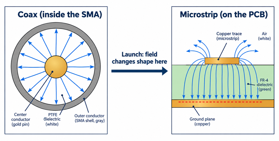
Figure 3: The electric field changing shape from coax to microstrip at an SMA launch
The return current matters as much as the signal. It flows back along the inside of the shell, then crosses into board ground through the connector legs and nearby vias. If the nearest via sits 3 mm (118 mil) away, the current takes a detour. That detour adds inductance exactly where the launch is already mismatched.
Impedance Matching and Signal Integrity
Impedance matching at the launch means keeping the entire path near 50 ohms, including the pad. A 1.27 mm (50 mil) pad on that dielectric measures roughly 22 ohms. The reflection coefficient is (22 - 50) / (22 + 50), or about -0.39. So, nearly 40% of the incident voltage is reflected at the pad's leading edge. At 500 MHz, though, the pad is so short that its two edges reflect nearly equal and opposite waves, which cancel each other out.
As frequency rises, the pad becomes a larger fraction of a wavelength, and the cancellation fails. That is why a launch can look clean on a 1 GHz sweep, yet its return loss falls steadily as the sweep climbs past about 2 GHz. Holding that pad in check is the practical side of impedance control in PCBs.
SMA Connector PCB Layout Considerations
SMA connector PCB layout comes down to three decisions: the trace-to-pin transition, the ground vias, and the footprint. The wider RF PCB layout guidelines still apply, but these three decide whether the launch holds 50 ohms.
Launch Design and Signal Path
Launch design starts by removing ground, not adding it. A void in the layer 2 plane beneath the pad, and sometimes in layer 3, shifts the pad's reference plane deeper, reducing its capacitance. In Altium's simulation, clearing layers 2 and 3 brought a 1.27 mm (50 mil) pad to 50 ohms. The top-layer coplanar gap widened only from 0.15 to 0.25 mm (6 to 10 mils).
A taper looks like the obvious fix, but in the same Altium work, an untuned taper gave worse return loss than the cutout alone, though still acceptable. The wedge adds capacitance of its own. Instead, route the trace straight into the pad as a grounded coplanar waveguide. Even experienced designers trip on these launch mistakes:
- Leaving solid ground under the pad turns it into a roughly 22 ohm capacitor on thin prepreg. Cut the plane under the pad on layer 2.
- Bending the trace near the pad stacks a corner discontinuity on top of the pads. Keep the trace straight for the first few millimeters, then use two 45-degree bends or an arc.
- Drawing the pad longer than the pin leaves an open copper stub past the pin tip. Trim the pad to the pin length plus a small solder margin.
- Flooding the center pin with solder forms a fillet that increases capacitance. A thin fillet that just wets the pin and pad is enough.
Ground Via Placement and Return Paths
Ground vias carry the return current from the connector's legs into the plane. So the first pair belongs directly under or beside each leg. Every extra millimeter between leg and via adds series inductance to the return path. At a few GHz, that inductance acts like a gap in the ground.
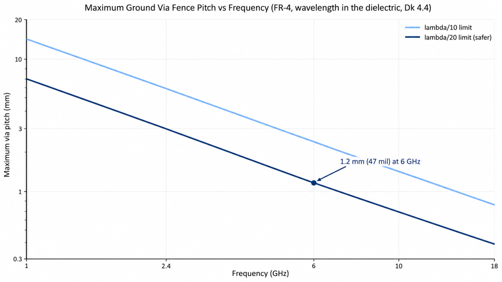
Figure 4: Maximum ground via fence pitch versus frequency on FR-4
A via fence ties the coplanar-side grounds to the plane, preventing parallel-plate mode from resonating between them. That mode lives wholly inside the dielectric. So the pitch follows the wavelength in FR-4 itself, about 24 mm (0.94 in) at 6 GHz for a Dk of 4.4. A fence at one-twentieth of that needs vias no more than 1.2 mm (47 mil) apart.
Footprint and Mechanical Alignment
The mounting style fixes the footprint, so choose it before drawing any copper. The four common styles differ in signal path quality and in how well they resist a pulling cable:
| Mounting Style | How It Attaches | Signal Path Quality | What It Means for Your Layout |
|---|---|---|---|
| Edge launch | Board edge sits between ground legs | Best, to 18 GHz with a tuned launch | Board thickness must match the part |
| Vertical through-hole | Pin and four legs in plated holes | Good, but the stub adds a discontinuity | Pin stub hangs below the trace layer |
| Vertical surface mount | Top-side pads only | Good, no stub | Weak against cable torque |
| Right-angle through-hole | Body parallel to the board | Lowest, bend plus stub | Saves height, costs margin |
Manufacturing RF PCBs for Reliable SMA Connections
A launch that simulates at 50 ohms only works if the fabricator builds the geometry you assumed. Dielectric heights, trace widths, and via positions all have tolerances, so the design must allow for them.
Controlling PCB Dimensions and Layer Structures
Dielectric height sets the 50-ohm trace width and, therefore, how closely the trace matches the pin. On a 2-layer 1.6 mm (63 mil) FR-4 board, a 50 ohm microstrip is about 2.8 mm (110 mil) wide. On a 0.51 mm (20 mil) RO4350B board, it is close to 1 mm (39 mil), almost the pin width. That is why thin Rogers boards launch so cleanly.
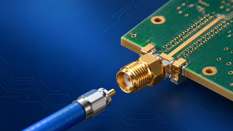
Figure 5: An edge-launch SMA connector clamped onto a 1.6 mm (63 mil) 4-layer PCB
JLCPCB maintains thickness within ±10% for 1.0 mm (39 mil) and above. A 1.6 mm (63 mil) board can therefore arrive at 1.44 to 1.76 mm (57 to 69 mil). Keep the connector datasheet open while choosing your PCB thickness, so the clamp fits the board you receive.
Maintaining RF Trace and Via Accuracy
Etching never produces the rectangle your field solver assumes. The etchant attacks sideways as it cuts down, so a finished trace comes out trapezoidal. At a 3:1 etch factor, a 1-oz trace ends about 25 µm (1 mil) narrower on top. On a 0.36 mm (14 mil) trace, that raises impedance by about an ohm, so fabs correct drawn widths from measured data.
Via accuracy matters most in the fence and at the launch. Drill position tolerance and layer registration shift each against the surrounding copper. So a fence drawn tight to the coplanar gap can end up touching it. Keep clearances at the values your impedance tool assumed, and size vias so a drill offset still leaves a full annular ring.
Inspection and Quality Verification
Impedance is verified on test coupons rather than on your board. The coupon sits within the panel border and undergoes the same etching and lamination. It is then measured by time-domain reflectometry under IPC-TM-650 method 2.5.5.7. JLCPCB tests impedance-controlled orders within a ±10% band, so a 50-ohm target falls within 45-55 ohms.
An RF sweep of the first assembled board is the only test that sees the launch as built. A network analyzer plot of S11, the reflected signal, indicates whether return loss remains within your band. If it does not, a TDR trace locates the fault. Once the board passes, order the production run on the same stackup and finish.
Common SMA Connector Applications
SMA connectors appear in two types of systems: test setups and wireless products. Test setups require repeatability across hundreds of matings, whereas a wireless port requires a clean match within a single band.
RF Testing and Measurement
Evaluation boards, filters, amplifiers, and test fixtures use SMA connectors because they mate with lab cables and instruments up to 18 GHz. An SMA also mates with precision 3.5 mm and 2.92 mm connectors. But a worn SMA pin can damage the costly port on a network analyzer, so mating follows a routine:
- Inspect the plug pin and jack face under magnification, as a bent pin can damage its mate.
- Fit a connector saver, a sacrificial adapter, on the instrument port.
- Align both halves and turn only the coupling nut, never the connector body.
- Finish with a preset SMA torque wrench so the mating plane repeats.
- Calibrate at the cable ends you will use, after the cables are routed.
The launch still sits inside every measurement you take. IEEE 370-2020 describes how to design test fixtures and remove them from the data, typically with a 2x-thru structure. As a result, the connector and launch effects can be subtracted from the measured S-parameters.
Wireless and High-Frequency Systems
In wireless products, the SMA connector is usually the antenna port, and the band sets how strict the launch must be. A 915 MHz LoRa radio tolerates a rough launch, whereas a 5 GHz Wi-Fi port needs a tight via fence:
| Application | Band | Connector | What It Means for Your Layout |
|---|---|---|---|
| LoRa and sub-GHz ISM radio | 868 / 915 MHz | SMA jack | FR-4 is fine; keep the ground continuous |
| GNSS receiver | 1.575 GHz (GPS L1) | SMA jack, DC on center pin | Antenna power shares the RF trace |
| Cellular modem | About 0.7 to 2.7 GHz (LTE); 5G adds 3.3 to 4.2 GHz | SMA jack | Check return loss at both band edges |
| Wi-Fi router | 2.4 / 5 GHz | RP-SMA jack | Via fence near 1.2 mm (47 mil) pitch |
FAQs About SMA Connectors
Q: Can an RP-SMA antenna connect to a standard SMA jack?
It threads on, but it does not connect electrically. RP-SMA swaps the pin and socket between halves, so an RP-SMA plug meets an SMA jack socket-to-socket. The center conductors never touch, so use matching variants or an adapter.
Q: Do I need a Rogers board for an SMA connector, or will FR-4 work?
FR-4 works for most designs up to a few GHz if the launch and vias are done properly. Its loss rises with frequency, so RO4350B makes sense for long RF traces or designs above about 6 GHz.
Q: What is the difference between an SMA connector and a U.FL connector?
U.FL is a tiny snap-on connector rated to about 6 GHz and roughly 30 mating cycles, so it suits links inside a product. SMA is larger and rated for about 500 cycles. That is why SMA serves as the external port, often fed from a U.FL pigtail.
Q: How tight should an SMA connector be?
Brass SMA connectors take about 3 to 5 in-lb (0.34 to 0.56 N·m). Stainless steel versions take about 7 to 10 in-lb (0.8 to 1.1 N·m). Use a preset torque wrench, because over-tightening deforms the pin and can crack the PTFE.
Q: Is a 26.5 GHz SMA connector worth it for a 2.4 GHz design?
Usually not, because a standard 18 GHz part already has ample margin at 2.4 GHz. At that frequency, the board launch and ground vias determine the return loss. Precision parts earn their cost near the top of the 18 GHz range and above.
Conclusion
An SMA connector provides a reliable connection between a 50-ohm coaxial cable and a PCB. However, good RF performance depends on more than the connector itself. The most critical area is the PCB launch, where the signal transitions from the connector to the board's transmission line. As more wireless devices adopt the 6 GHz Wi-Fi band, careful SMA connector layout becomes increasingly important, particularly for high-frequency PCB designs.
To achieve reliable RF performance, follow the connector manufacturer's recommended footprint and use a controlled-impedance PCB stackup. JLCPCB offers impedance-controlled PCB manufacturing and Rogers material options for RF applications. Its component library also includes PCB-mount SMA connectors, helping designers source components for their projects.

Keep Learning
Understanding Multilayer PCB Stackup
Key Takeaways Layer Arrangement: Optimize signal, ground, and power layer placement for better performance. Material Selection: Choose suitable core, prepreg, and copper materials. Signal Integrity: Control impedance and minimize crosstalk and EMI. Stackup Design: Use symmetrical structures to reduce warpage risks. Manufacturability: Consider layer count, via structures, and manufacturing limits early in design. Performance & Cost: Balance electrical requirements, reliability, and production costs. In......
Designing Antennas on PCB: A Beginner to Advance Guide
In today’s world of widespread wireless connectivity, the demand for small, affordable, and reliable antennas is higher than ever. Antennas act as real-world implementations of electromagnetic wave principles. They enable the sending and receiving of signals for a variety of wireless uses. While there is a lot of theoretical and experimental research in this area, only a few designs become widely used in actual products. Among the different options, Printed Circuit Board (PCB) antennas have become a p......
PCB Antenna Design: Types, Principles, and Best Practices
In the world surrounded with wireless communication, the demand for compact, inexpensive and reliable antennas has never been higher. Antennas are the application of electromagnetic waves. There are many theories and practicals available on antennas, but only few of them get recognised. For wireless data transfer the one solution can be usage of Printed Circuit Board (PCB) antennas. Using PCB antennas represents a convenient solution for integrating them directly into electronic devices, eliminating t......
Effective Escape Routing Strategies for High-Density BGA Success
Key Takeaways Escape routing is essential for successfully fanning out high-density BGAs, especially at 0.5 mm pitch and below. Use dogbone fanout for ≥0.5 mm; switch to via-in-pad (filled & capped) for finer pitches. HDI microvias and stacked vias significantly improve routing density and reduce layer count. Maintain symmetry and short stubs for differential pairs to preserve signal integrity. Combine smart stackup, DFM checks, and capable fabrication for reliable, high-yield results. Ever put a 484-......
ESP32 BLE Guide: Choosing the Right Chip and Designing Your PCB
Key Takeaways ESP32 BLE support: Most ESP32 chips support Bluetooth Low Energy (BLE), except the ESP32-S2, which supports only Wi-Fi, and the ESP32-P4, which has no built-in wireless radio. The original ESP32 also supports Bluetooth Classic, while newer models offer Bluetooth 5 features. Wi-Fi and BLE coexistence: Wi-Fi and BLE share the same 2.4 GHz radio and take turns using it. Heavy Wi-Fi activity can reduce BLE throughput or interrupt scanning, so both functions need to be tested together. Power ......
How SMA Connectors Work in RF PCB Design
Key Takeaways Focus on the Launch: Signal loss happens where coax turns into a flat trace, not inside the SMA body. Clear Ground Under Pads: Cut ground planes under launch pads to control capacitance and keep 50 ohms. Place Ground Vias Close: Put ground vias next to connector legs to shorten return paths. Account for Tolerances: Trace etching and board thickness directly alter launch impedance. Handle with Care: Use a torque wrench on joints and switch to high-frequency boards above 6 GHz. An SMA conn......