How Etch Factor Control Ensures Precise Trace Width and Reliable PCB Performance
13 min
- The Etch Factor Formula and Its Practical Use
- Impact of Etch Factor on PCB Design and Performance
- Professional Manufacturing Techniques for Optimal Etch Factor
- JLCPCB's Expertise in Etch Factor Management
- FAQ about Etch Factor Control
- Conclusion
Key Takeaways
Mastering etch factor control is essential for achieving precise trace width and reliable PCB performance. By understanding the etch factor formula and effectively managing undercut during the chemical etching process, designers and manufacturers can minimize trace width deviation, maintain accurate impedance, and ensure high-yield production — especially critical for fine-line, high-speed, and controlled-impedance designs.
Ever designed a PCB with a perfectly calculated width for traces, only to get back a manufactured board with traces that are a bit narrower than you had planned for? The reason is that the parameter that is almost always responsible for this is the Etch Factor, which is a fundamental parameter used in the PCB manufacturing process, and which determines how well your design is transferred to the copper on the board. Etch factor is the ratio in simple numbers that explains the relationship between the vertical etching (the depth of copper that is etched away) and the lateral etching (the undercut of copper that is etched away under the etch resist). When exposed to the chemical etching liquid, the liquid doesn't just eat out the copper vertically. It also feeds laterally beneath the resist layer, forming a trapezoidal shape rather than the desired rectangular shape.
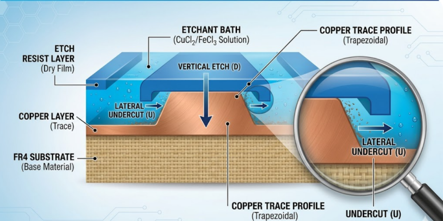
It is an undercut phenomenon that cannot be avoided in subtractive etching. All PCB manufacturers have to cope with it, and the etch factor measures the amount of lateral erosion compared to the amount of etch that's supposed to happen. The higher the etch factor, the less undercut and the sharper the walls, exactly what you want when designing a tight tolerance design.
The Relationship Between Etch Factor and Trace Accuracy
There is a direct and measurable relationship between the etch factor and the final trace size that will be obtained. The etching of 1oz (35um) Copper is a through-etch process, where the etchant attacks the copper in a straight line, all 35um deep. But at the same time, it undercuts horizontally on both sides of the trace. For example, if the etch factor is 3.0, then the lateral undercut is etch depth/3 or approximately 11.7 um per side.
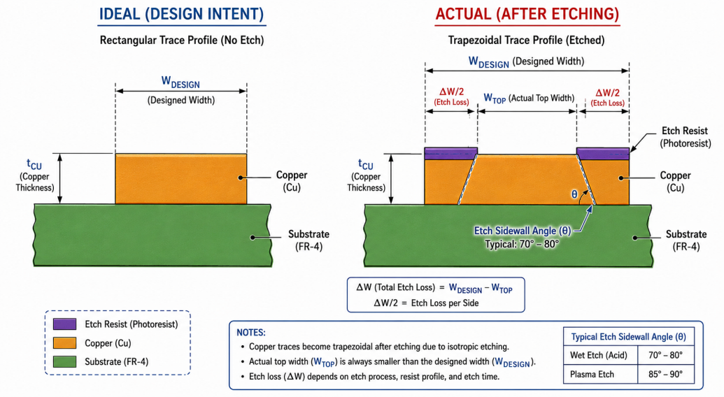
This equates to a loss of 23.4 um of the total width of your trace from the artwork dimensions. If you wanted to make a 150 um (around 6 mil) trace, you'd end up with 127 um, which is pretty far off and can affect impedance and current capabilities. That's why it's essential to know what etch factor is in the PCB making process when precision design is required. You can use it to directly know if your controlled-impedance traces, fine-pitch BGA escape routing, and RF transmission lines will hit your target specifications. The more stringent the design tolerances, the more critical the control of the etch factor.
The Etch Factor Formula and Its Practical Use
How to Calculate Etch Factor
The etch factor formula is simple, but it does need to be interpreted correctly to use it.
The formula is: Etch Factor (EF) = D / U
Where:
D = Etch depth (vertical) = copper thickness to be removed
U = Undercut (lateral), the lateral (horizontal) distance the etchant has moved under the resist on one side
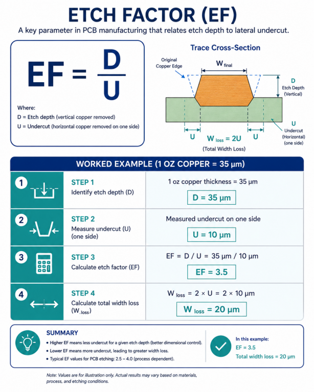
This expanded relationship is more practical and can be directly related to the width of the trace: U = D / EF
Total trace width loss = 2 x U = 2D / EF
Designed width – (2D / EF) = Final trace width
Let's go through an actual calculation. You are etching 1 oz copper (35 um thick), and your etch factor is 3.5:
- Etch depth (D) = 35 µm
- Undercut per side (U) = 35 / 3.5 = 10 µm
- Total width loss = 2 x 10 = 20 um
- If your designed trace is 200 um, the final trace = 200 - 20 = 180 um
This is the calculation that the manufacturers are applying to compensate for the artwork. If the final required trace width is 180 μm, then the fabricator sets the artwork to 200 um, and pre-compensates for the undercut. It is a standard practice of any professional PCB facility to do this type of compensation during CAM processing.
Factors That Influence the Etch Factor in Production
The etch factor is not always a constant. Depending on various process parameters, there are variations, and it's controlling these parameters that differentiates the high precision manufacturer from the basic one. The main reasons are the following:
| Factor | Effect on Etch Factor | Typical Range |
|---|---|---|
| Copper thickness | Thicker copper = more undercut time = lower EF | 0.5 oz to 6 oz (17-210 um) |
| Etchant type | Alkaline vs. acidic chemistry affects undercut profile | EF 2.5-4.0 depending on chemistry |
| Etchant concentration | Higher concentration can improve directionality | Application-specific |
| Conveyor speed | Faster speed = less dwell time = different undercut ratio | 1.0-3.5 m/min typical |
| Spray pressure | Higher pressure improves fresh etchant delivery | 1.5-3.0 bar typical |
| Nozzle design | Cone vs. fan nozzles affect etchant distribution | Manufacturer-specific |
| Temperature | Higher temp = faster etch, but potentially more undercut | 45-55 degrees C typical |
| Copper type | ED copper vs. rolled copper etch differently | Grain-structure dependent |
The interplay between these factors means that achieving a consistently high etch factor requires precise process control. Even small variations in etchant temperature or spray pressure can shift the undercut profile and change your final trace dimensions.
Impact of Etch Factor on PCB Design and Performance
Effects on Impedance Control and Signal Integrity
This is where the etch factor is no longer a manufacturing parameter and becomes a design critical parameter. The trace width is one of the key parameters in the equation that determines the impedance of controlled-impedance PCBs. Even slight variations in the desired width can cause impedance to go outside allowable tolerances.
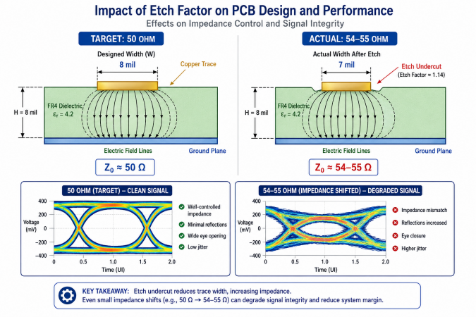
The trapezoidal cross-section resulting from etching an undercut also has an impact on the impedance, which is different from a perfect rectangular cross-section. Trapezoidal trace models have been added to most impedance calculators because nowhere is the etch profile a perfect rectangle. The lower part of the trace (near the etch resist) is correspondingly wider than the top, and the difference in width is a factor that should be considered in any precise modeling of the impedance. It is even more critical for differential pairs. Etch Factor will impact the width of the trace as well as the gap between the traces. When the undercut reduces the trace width and increases the gap width at the same time, the differential impedance will change more than the single-ended impedance will.
Common Issues Caused by Poor Etch Factor Control
If the etch factor is not controlled, various issues propagate along the manufacturing process and into the end product:
- Impedance deviation: Trace width errors, as mentioned above, directly result in impedance mismatches and therefore in reflections and poor eye diagrams in high-speed links.
- Affects current capacity: Narrower trace impedance is less than designed. This can lead to excessive voltage drop of the trace or even trace burnout when put under load by the power delivery network.
- Spacing violations: the width of traces decreases, and the spacing between traces increases. This could be harmless, but the actual spacing is different than the design, and/or in some situations, the trace width may be less than the minimum width requirements.
- Undercut causing open circuit on fine features: For very fine traces (3-4 mil), too much undercut can result in complete etching through the narrow features, resulting in an open circuit and loss of function.
- Variation of etch factor over a production panel: This may cause the trace width and/or impedance to be different on different boards on the same panel.
- Yield loss and rework: Boards that fail impedance testing or continuity testing because of etch factor problems must be scrapped, which increases production costs.
It's not just a theoretical issue. These are actual manufacturing issues that PCB fabricators face every day, particularly as design rules get smaller than 4 mil trace and space.
Professional Manufacturing Techniques for Optimal Etch Factor
Advanced Etching Process Control and Parameter Optimization
In order to achieve as little undercut as possible and as accurate traces as possible, modern PCB fabrication processes have a few smart tricks. Optimization of the spray system is the first line of defense. The angle, pressure, and pattern of the etchant spray nozzle(s) directly influence the contact of the etchant to the copper surface. Those fan-shaped nozzles at an optimized angle (usually 15-30 degrees from vertical) facilitate the delivery of a fresh etchant to the front of the etch while removing spent etchant. Further uniformity over the panel width is obtained through oscillating nozzle arrays.
Etchant management systems constantly monitor and control the chemical bath. Key parameters include:
- Etchant specific gravity (concentration), which is kept within a narrow process window with automated dosing
- Control of temperature (usually set at 50 +- 2 degrees C for even reaction rate)
- pH monitoring is particularly important when using alkaline etchants (ammoniacal cupric chloride).
- The dissolved copper concentration in the solution influences the etching speed and needs to be controlled by regeneration/replacement of the solution.
- Precise timing of the etch endpoint to avoid over-etching
Dwell time in the etch chamber can be controlled by the conveyorized processing and variable speed control. This, combined with real-time feedback from an optical inspection system, forms a closed-loop process, which adapts to changing conditions during a production run.
Material and Chemistry Choices for Better Results
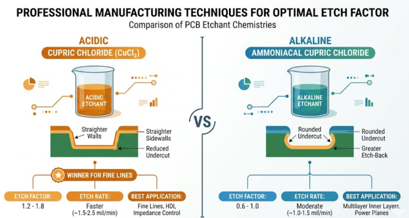
The etch factor is very dependent upon the etch chemistry used. There are two widely used etchant systems in the PCB manufacturing industry, each of which has unique properties:
| Property | Cupric Chloride (Acidic) | Ammoniacal Cupric Chloride (Alkaline) |
|---|---|---|
| Typical etch factor | 3.0-4.0 | 2.5-3.5 |
| Etch rate | Moderate | Fast |
| Undercut profile | Straighter sidewalls | More rounded undercut |
| Regeneration | Easy (HCl + oxidizer) | Complex (ammonia balance) |
| Best for | Inner layers, fine lines | Outer layers with tin/lead resist |
| Environmental handling | Simpler waste treatment | Ammonia emission controls needed |
| Copper compatibility | Works with all resists | Requires metallic resist (Sn, Sn/Pb) |
For fine-line inner layer etching, the etched sidewall profiles tend to be straighter with a higher etch factor when using acidic cupric chloride. Alkaline etchants are more often used for outer layers in which tin or tin-lead resist is applied following pattern plating.
In addition to etchant chemistry, the type of copper foil is important. Because the grain structure of reverse-treated foil (RTF) and very-low-profile (VLP) copper etch is smoother, it can be etched laterally in a more predictable pattern than standard electrodeposited copper, resulting in a more uniform etch. These specialty foils can help achieve an etch factor improvement of 10-15% over standard foils, and are ideal for high-density interconnect (HDI) designs with 3/3 mil or finer trace and space.
JLCPCB's Expertise in Etch Factor Management
Precision Etching Equipment and Tight Process Control
If you need to convert the design into desired copper features, JLCPCB has cutting-edge etching lines and process control systems. Their conveyorized etching equipment has optimized nozzle configuration, controlled spray angle, and pressure, which provides a uniform etchant supply for the full surface of the panel.
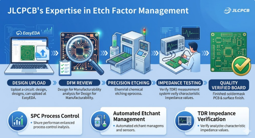
JLCPCB's process control infrastructure features automated etchant management systems, which automatically monitor etchant concentration, temperature, and copper loading. This real-time monitoring, together with Statistical Process Control (SPC) techniques, maintains the etch factor within narrow and repeatable control limits that are critical for providing repeatable trace widths throughout production volume. JLCPCB's integration with EasyEDA also streamlines this process. You can design your PCB, perform DRC, and send for fabrication all in one ecosystem. Using the instant quoting system, your copper weight, trace widths, and impedance requirements are taken into account, and the etch factor compensation is incorporated into the manufacturing plan from the beginning.
Consistent High-Yield Production with Reliable Trace Dimensions
The high-quality equipment, optimized chemistry, and process control enable JLCPCB to assure uniformity of trace dimensions at any production volume. The etch factor performance is the same for an order of 5 prototype boards or 5,000 production boards. JLCPCB offers impedance test coupons for controlled impedance orders on the production panel. These coupons are measured with TDR (Time Domain Reflectometry) equipment to ensure that the etched trace widths translate to the desired impedance. In this closed-loop verification process, any etch factor variations (should they occur) are detected and corrected prior to shipment of your boards.
FAQ about Etch Factor Control
Q: What is the etch factor in PCB manufacturing?
Etch factor is the ratio of the vertical etch depth (copper thickness removed) to the horizontal undercut on one side of a trace. It quantifies how much sideways erosion occurs during the chemical etching process. A higher etch factor means less undercut and more accurate trace widths.
Q: How do you calculate etch factor?
The etch factor formula is EF = D / U, where D is the etch depth (copper thickness), and U is the lateral undercut on one side. For example, if you etch through 35 um of copper and the undercut is 10 um per side, the etch factor is 35 / 10 = 3.5.
Q: What is a good etch factor value?
A typical etch factor in production ranges from 2.5 to 4.0, depending on the etchant chemistry, copper thickness, and process parameters. For fine-line designs (below 4 mil trace and space), an etch factor of 3.5 or higher is desirable to maintain trace width accuracy.
Q: Does copper thickness affect etch factor?
Yes, copper thickness is one of the most significant factors. Thicker copper requires longer etching time, which allows more lateral undercut to accumulate. This is why fine-line designs typically use thinner copper (0.5 oz or 1 oz) to achieve better etch factor performance.
Q: How does the etch factor affect impedance?
Etch factor directly affects trace width, which is a primary variable in impedance calculations. Poor etch factor control can cause traces to be narrower than designed, shifting impedance higher than the target value.
Conclusion
One of those manufacturing parameters that works behind the scenes, the etch factor can have a significant effect on the quality of your end product. Whether your board will perform as intended depends directly on the etch factor, from trace width accuracy to impedance control and signal integrity to manufacturing yield. Familiarity with the etch factor formula and the factors that affect it will enable you to make better design decisions. You can reduce this difference between the design intent and the manufactured product by using an appropriate copper weight for your feature size, by designing for the expected undercut, and by using a manufacturer that values process control. Etch factor control will be even more important in the future as PCB designs continue to become finer and tighter.
Keep Learning
How Laser-Made PCBs Are Used in Rapid Prototyping
Key Takeaways Speed & Precision: Digital lasers enable 24-hour quick-turn HDI and FPC prototyping without mechanical tooling. LDI Patterning: Replaces physical photo-films to deliver precise circuit traces down to 2/2 mil. HDI Microvias: UV/CO2 lasers drill 0.075–0.15 mm blind vias (1:1 aspect ratio) for 1+N+1 to 3+N+3 stackups. Laser Profiling & Stencils: Achieves ±0.05 mm FPC cut accuracy and ±0.003 mm LPKF stencil aperture precision. Laser DFM: Maintain ≥ 0.30 mm copper clearance on FPCs and ≥ 0.07......
A Beginners Guide to Tented vs Untented Vias
Via’s are important, If working at high speed design and HDI boards then they become super important. Choosing a type of via during PCB manufacturing matters. Via’s are basically joining two or more layer traces together. Shape, size and track length guidelines became more interesting at high frequency and high speed signals. Today in this article we will explore a fabrication side, the decision to use tented or untented vias. This beginner-friendly guide explains what tented vias are, the differences......
Understanding SMT PCB Boards Technology: An Essential Component of Modern Electronics
Surface Mount Technology (SMT) has changed manufacturing of modern electronics. It has made designs and assembly methods more efficient. Many modern electronics depend on SMT PCB boards, which make it possible for circuit designs to be small and efficient. This is what today's technology needs. This article discuss about many types of SMT PCB boards, their uses, and the best methods for designing and assembling them. 1. What is an SMT PCB Board? Printed circuit boards called SMT PCB boards, use surfac......
How to Choose the Right Prepreg Material for Reliable Multilayer PCB
Have you ever wondered what makes all those copper layers stick to a cross-section of a multilayer PCB? Prepreg material is the answer, and it is of much more importance than most engineers think it is. Choose the prepreg selection wrong, and you are predetermined to delamination, impedance drift, and long-term reliability problems. Prepreg is not only glue. It is a designed composite that determines your dielectric separation, dictates your impedance, affects signal loss, and determines your board be......
Via Filling Explained: Key Techniques, Benefits, and Solutions for High-Performance PCBs
Key Takeaways Via filling completely fills plated through-holes and microvias with epoxy or conductive copper paste, followed by planarization and copper capping (POFV). It eliminates voids, solder wicking, and thermal/mechanical issues while enabling reliable via-in-pad designs. Benefits include superior heat dissipation (up to 8 W/m·K), better signal integrity, higher mechanical strength, and improved assembly yields. JLCPCB provides free non-conductive filling + POFV on 6+ layer boards. Ideal for H......
How Fiducial Markers Guarantee Perfect Alignment in Professional PCB Fabrication
Today, the most sophisticated pick-and-place machine can place a 0.5 mm pitch QFP on its footprint, board after board, thousands of times, and never miss. It is not only a matter of expensive cameras or high-quality servos, but it begins with a little, very small copper dot, simply hanging there in the corner of your PCB. That dot represents a fiducial marker, and without it, even the smoothest SMT line would be laying components in the dark. The unrecognized heroes of automated assembly are the fiduc......