PCB Encapsulation: Design Rules, Material Selection, and Reliable Manufacturing
10 min
- What is PCB Encapsulation and Why Is It Critical?
- PCB Encapsulation vs. Conformal Coating: Which One Do You Need?
- Key Resin Materials for PCB Encapsulation
- DFM Rules: Designing PCBs for Successful Encapsulation
- High-Reliability PCBA Manufacturing: How JLCPCB Ensures Encapsulation Success
- FAQ about PCB Encapsulation
- Conclusion on PCB Encapsulation
Key Takeaways
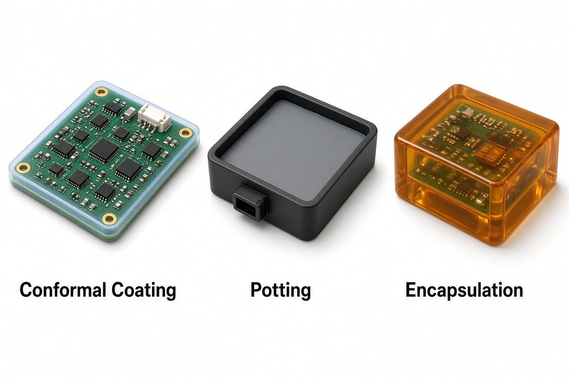
- Encapsulation vs. Potting: Potting uses a permanent shell; encapsulation produces a free-standing resin-coated module. Both deliver full environmental isolation.
- Encapsulation vs. Conformal Coating: Conformal coating is lightweight and reworkable but limited to mild environments. Encapsulation provides IP67/IP68 submersion-grade protection at the cost of repairability.
- Resin Selection: Epoxy offers rigidity and chemical resistance; polyurethane provides flexibility for thermal cycling; silicone excels in high-temperature environments from -50C to 200C+.
- DFM Considerations: Maintain sufficient component clearances, orient packages inline with resin flow, and implement physical dams to prevent resin migration into keep-out zones.
- Manufacturing Partnership: Clean, precision-assembled PCBs with rigorous inspection (AOI, X-ray) form the foundation for successful encapsulation outcomes.
What is PCB Encapsulation and Why Is It Critical?
Modern electronic assemblies operating in harsh environments require robust protection against moisture, thermal shock, mechanical vibration, and corrosive chemicals. PCB encapsulation provides an impermeable barrier by housing or submerging the circuit assembly in liquid polymer resins that cure into durable solids. Engineers must evaluate material properties, mechanical tolerances, and Design for Manufacturability (DFM) guidelines to ensure high yield and long-term reliability.
PCB Encapsulation vs. PCB Potting: Clarifying the Terms
PCB encapsulation and PCB potting are often used interchangeably, but they refer to specific process variations in electronic packaging. Potting involves placing the assembled PCB into a permanent shell or enclosure, pouring liquid resin to fill all voids, and leaving the housing as part of the final product. Encapsulation, in a strict sense, involves dipping or molding the assembly in a removable shell or tool, resulting in a free-standing, resin-coated module once cured. Both techniques deliver complete physical encapsulation, ensuring structural integrity and zero air gaps around critical components.
Primary Benefits of Encapsulating Printed Circuit Boards
Encapsulating a circuit assembly provides complete environmental isolation, high mechanical damping, and improved electrical insulation. The solid resin block prevents moisture ingress, salt spray accumulation, and chemical attack, making it indispensable for automotive, industrial, and outdoor IoT applications. Furthermore, encapsulating fragile surface-mount devices (SMDs) shields solder joints from mechanical fatigue caused by severe vibration or shock.
Key operational advantages include:
- Complete environmental sealing (IP67/IP68 rating capability).
- Absorption of high mechanical vibration and physical impact.
- Increased dielectric resistance for high-voltage power electronics.
- Thermal dissipation management when loaded with conductive fillers.
PCB Encapsulation vs. Conformal Coating: Which One Do You Need?
Choosing between PCB encapsulation and conformal coating depends on the severity of operating environments and weight restrictions. Conformal coatings apply a thin film (typically 25 to 75 microns) that follows the contours of the board, whereas encapsulation forms a thick mass (often several millimeters to centimeters) that completely submerges components.
Performance Comparison Matrix
Conformal coating offers lightweight protection against light condensation and dust, but it falls short under prolonged submersion, high mechanical shock, or heavy chemical exposure. PCB encapsulation provides absolute barrier protection capable of surviving IP67/IP68 immersion ratings, heavy vibration, and high voltage differentials. The following table highlights the operational trade-offs between these two protection strategies:
| Property / Parameter | Conformal Coating | PCB Encapsulation / Potting |
|---|---|---|
| Typical Thickness | 25 m to 125 m | 1 mm to >15 mm |
| Mechanical Shock Resistance | Low to Moderate | Exceptional (Vibration damping) |
| Moisture & Submersion | Resistance to humidity/splashes | Full submersion (IP67/IP68) |
| Weight Impact | Minimal (less than 5 grams per board) | Significant (Adds resin mass) |
| Dielectric Isolation | Up to 1.5 kV | High voltage (greater than 10 kV) |
| Repairability / Rework | Easy (Solvent or heat removal) | Very Difficult / Non-reworkable |
Cost and Process Trade-offs
While conformal coating reduces material consumption and keeps overall assembly weight low, encapsulation involves higher resin volumes and longer curing cycles. However, for assemblies subject to extreme environments, the higher upfront process cost of encapsulation prevents catastrophic field failures and costly warranty claims. Engineers must weigh the non-reworkable nature of encapsulated boards against the operational risk of exposure, ensuring that circuit testing is performed before the resin is poured and cured.
Key Resin Materials for PCB Encapsulation
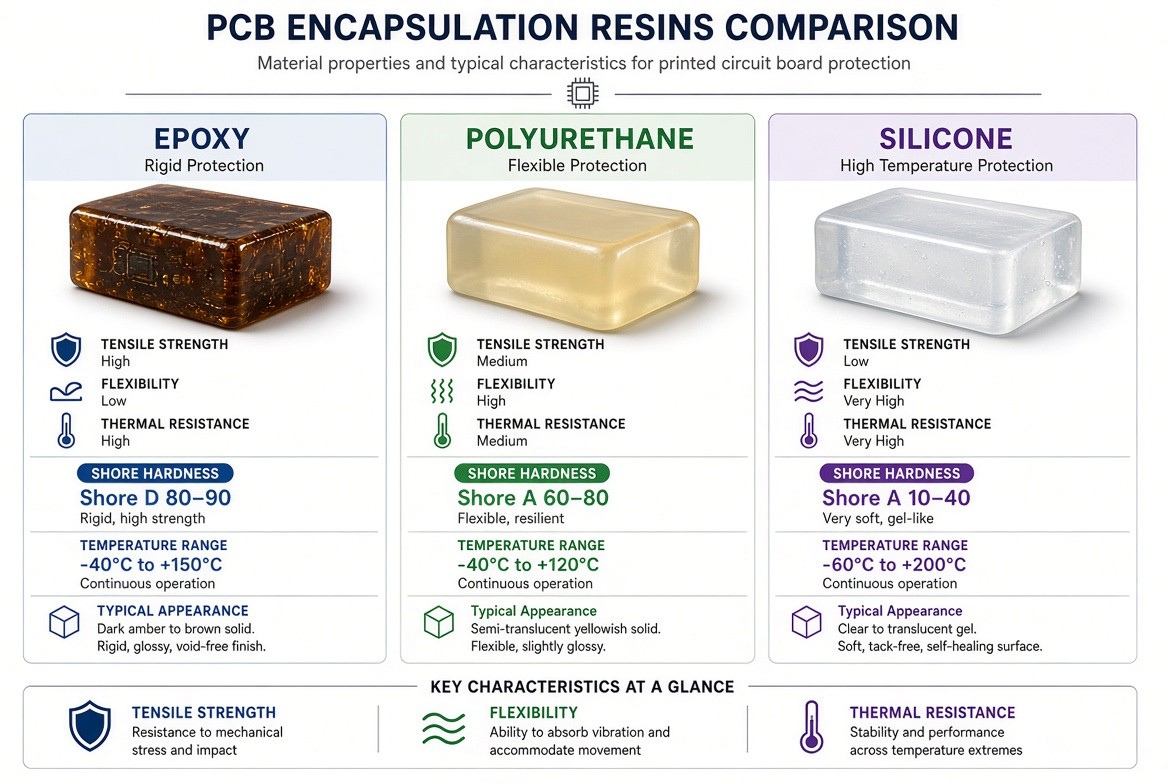
Selecting the correct resin compound requires balancing mechanical hardness, thermal conductivity, operating temperature range, and curing shrinkage. Epoxy, polyurethane, and silicone represent the three dominant chemical families used in industrial electronics.
1Epoxy Resins (EP)
Epoxy resins deliver high mechanical strength, excellent chemical resistance, and strong adhesion to FR-4 substrates and metallic components. They feature high tensile strength and rigid structural protection, making them ideal for high-impact industrial modules. However, epoxies exhibit higher shrinkage during thermal curing, which can exert stress on delicate surface-mount components or fine-pitch solder joints during temperature cycling.
2Polyurethane Resins (PU)
Polyurethane compounds offer a flexible protective layer with superior resistance to cracking at low operating temperatures. Their elastomeric properties make them an excellent choice for assemblies subjected to rapid thermal cycles or severe physical vibration. While polyurethanes provide great moisture resistance, their maximum continuous operating temperature is generally lower than that of epoxies and silicones, typically capped around 120C to 130C.
3Silicone Compounds
Silicone encapsulants excel in high-temperature environments, retaining flexibility across a broad temperature range from -50C to above 200C. They exhibit the lowest shrinkage during cure and impose minimal mechanical stress on delicate components like ceramic chip capacitors or fine wire bonds. The primary trade-offs of silicone resins are higher raw material costs and lower resistance to certain aggressive petroleum solvents compared to epoxies.
| Polymer Family | Tensile Strength | Shore Hardness | Temp Range (C) | Moisture Resistance |
|---|---|---|---|---|
| Epoxy (EP) | High (50-80 MPa) | D80 - D90 (Rigid) | -40 to +150 | Excellent |
| Polyurethane (PU) | Medium (10-25 MPa) | A60 - D60 (Flexible) | -50 to +125 | Very Good |
| Silicone (SI) | Low (1-5 MPa) | A20 - A60 (Soft/Gel) | -50 to +200+ | Excellent |
DFM Rules: Designing PCBs for Successful Encapsulation
Design for Manufacturability (DFM) for PCB encapsulation requires proactive layout adjustments in the CAD environment to prevent trapped air pockets, component stress, and fluid leakage. Proper spatial planning ensures uniform resin flow and structural reliability.
Component Layout and Clearance Considerations
Components must be arranged with sufficient clearance to allow high-viscosity resins to flow beneath tall packages and around dense pin arrays. Trapped air bubbles create internal voids that degrade dielectric strength and cause localized thermal hotspots. Designers should maintain at least 1.5 mm spacing between tall components, align taller packages parallel to the primary resin flow direction, and avoid creating narrow channels where capillary action might trap air.
Specific rules include:
- Maintain minimum 1.5 mm clearance between adjacent high-profile components.
- Orient long rectangular packages inline with liquid resin dispensing paths.
- Avoid placing small 0402/0201 passives directly under overhanging heat sinks or modules.
Damming and Housing Design Integration
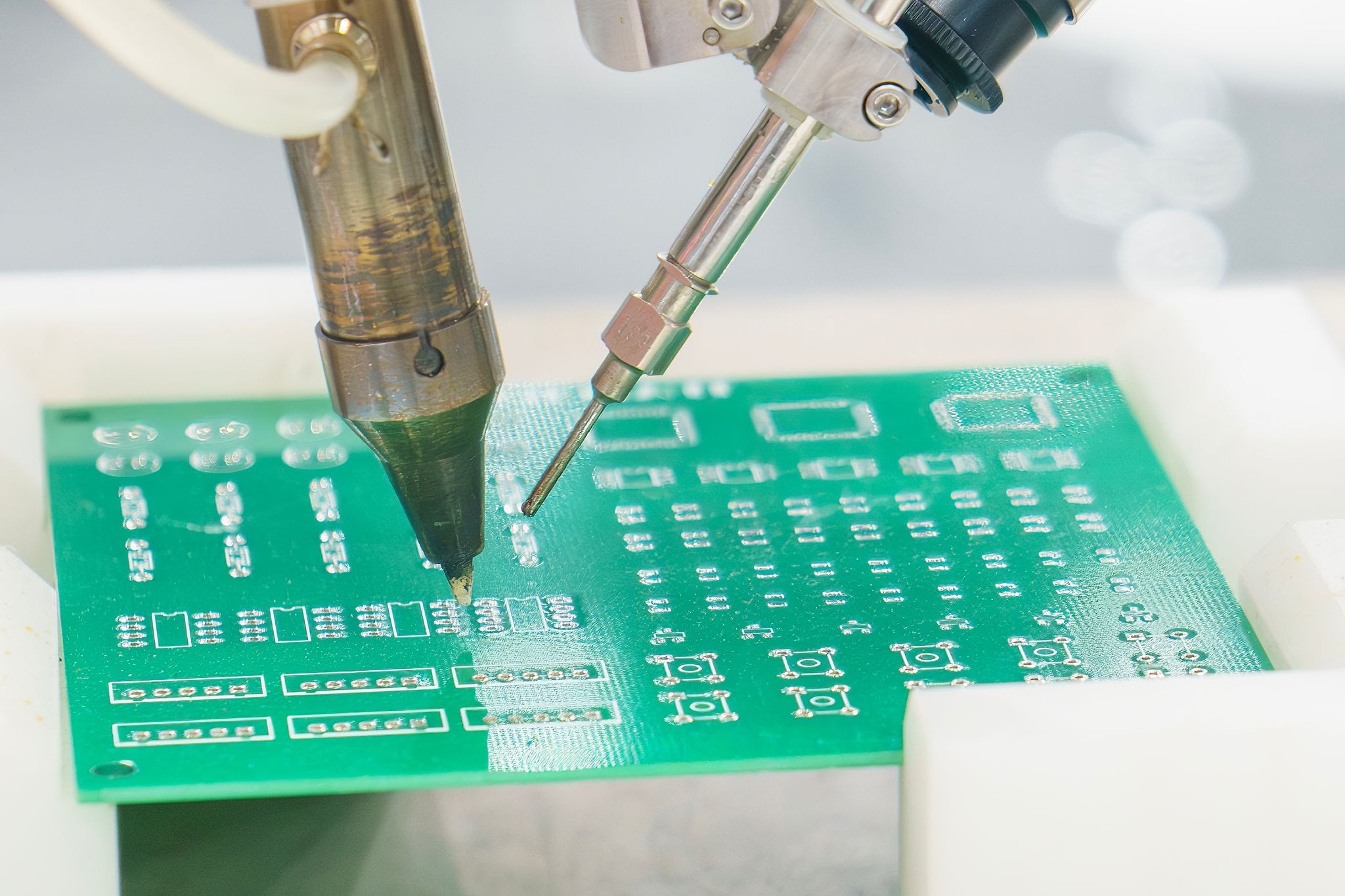
When executing localized encapsulation without a full enclosure, physical dams or barrier walls must be incorporated into the layout or housing. Uncontrolled resin flow can migrate into keep-out zones, such as board-to-board connectors, test points, switches, or optical sensors. Implementing silk-screen solder mask dams, milled slots, or molded plastic barriers ensures the liquid compound remains confined to designated areas during the potting process.
High-Reliability PCBA Manufacturing: How JLCPCB Ensures Encapsulation Success
Achieving consistent results in PCB encapsulation depends heavily on the quality, surface cleanliness, and precision of the underlying PCBA fabrication. JLCPCB integrates rigorous manufacturing controls to prepare circuit assemblies for reliable resin integration.
Precision SMT Assembly and Cleanliness Standards
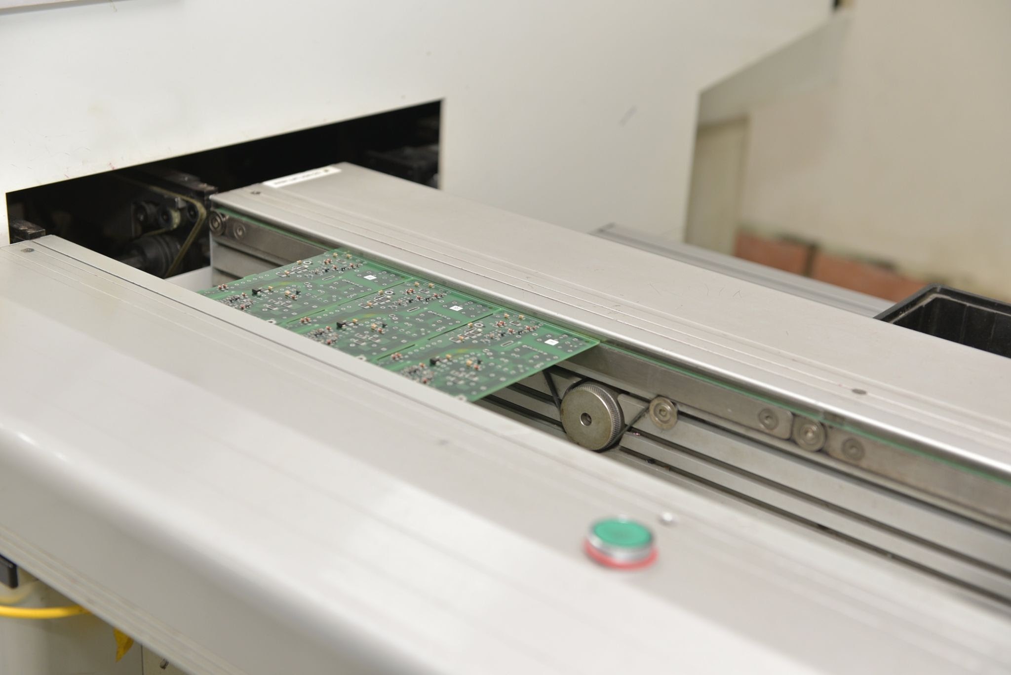
Clean PCB surfaces are crucial for achieving chemical adhesion between the encapsulating resin and the board assembly. Residual solder fluxes, organic contaminants, or dust particles can cause delamination, allowing moisture pathways to form over time. JLCPCB utilizes high-precision SMT placement equipment, optimized reflow temperature profiling, and automated optical inspection (AOI) to deliver clean, defect-free assemblies. Surface ionic cleanliness is monitored to ensure robust polymer bonding across FR-4 substrates, solder masks, and component bodies.
Seamless Transition from Prototype to Mass Production
Transitioning from initial prototype testing to volume manufacturing requires strict process consistency and automated DFM verification. JLCPCB provides free, automated DFM checks during file submission, identifying spacing violations, thermal copper distribution issues, and component clearance conflicts before production begins. From quick-turn prototype SMT runs to full-scale PCBA production, fully traceable manufacturing ensures every board meets IPC-A-610 Class 2 or Class 3 standards prior to encapsulation.
Key JLCPCB capabilities supporting encapsulated designs:
- High-density SMT placement accuracy down to 0.035 mm.
- Strict IPC Class 2 and Class 3 manufacturing standards.
- Automated Optical Inspection (AOI) and X-ray inspection for BGA/QFN underfill validation.
- Seamless online Gerber/BOM analysis for instant DFM feedback.
FAQ about PCB Encapsulation
Q: What is the difference between PCB encapsulation and conformal coating?
Conformal coating applies a thin film (25-75 microns) that follows the board contours, offering lightweight protection against humidity and dust. PCB encapsulation forms a thick solid resin block (1mm to >15mm) that completely submerges components, providing IP67/IP68 submersion-grade protection, superior mechanical damping, and high-voltage dielectric isolation at the cost of repairability.
Q: Which resin material is best for high-temperature PCB encapsulation?
Silicone compounds are the top choice for high-temperature applications. They maintain flexibility across a range from -50C to above 200C, exhibit the lowest shrinkage during cure, and impose minimal mechanical stress on delicate components. For applications below 150C, epoxy resins offer higher mechanical strength at a lower material cost.
Q: Can encapsulated PCBs be repaired or reworked?
Encapsulated PCBs are generally non-reworkable. The cured resin forms a solid, impermeable block that cannot be removed without damaging components. This is why thorough circuit testing must be completed before applying the encapsulation resin. In contrast, conformal coatings can be removed using solvents or heat for rework access.
Q: What DFM rules should I follow when designing a PCB for encapsulation?
Maintain at least 1.5mm clearance between tall components, orient rectangular packages inline with the resin flow direction, avoid placing small passives under overhanging structures, and incorporate physical dams or barrier walls around keep-out zones such as connectors, test points, and optical sensors to prevent resin migration.
Q: When should I choose PCB potting over encapsulation?
Choose potting when the assembly needs a permanent protective shell integrated into the final product housing, and when the shell itself provides mechanical mounting or environmental sealing. Choose encapsulation when you need a free-standing, resin-coated module without a permanent outer shell, such as for embedded sensor nodes or compact IoT devices.
Q: How does JLCPCB support high-reliability PCB encapsulation projects?
JLCPCB provides high-precision SMT assembly, automated DFM verification during file submission, IPC-A-610 Class 2/3 manufacturing standards, AOI and X-ray inspection, and rigorous surface cleanliness monitoring. These quality controls ensure every board is optimally prepared for reliable resin encapsulation from prototype to volume production.
Conclusion on PCB Encapsulation
PCB encapsulation remains one of the most effective strategies for protecting electronic assemblies against harsh physical, chemical, and thermal environments. Success requires balancing material characteristics like epoxy rigidity, polyurethane flexibility, and silicone thermal stability against practical DFM considerations such as component clearances and barrier damming. Partnering with an experienced manufacturer like JLCPCB guarantees high-precision board fabrication, clean SMT assembly, and strict quality control, establishing a solid foundation for long-term product reliability.
Keep Learning
Choosing the Right Surface Finish for Your PCB: An Overview of HASL, ENIG, OSP, Immersion Tin and Immersion Silver
Key Takeaways Lead-Free HASL: Best low-cost, RoHS-compliant finish for general PCB builds. ENIG: Superior flatness and 12+ month shelf life for fine-pitch BGAs. OSP: Ultra-flat, lowest-cost option for high-volume SMT (3–6 month shelf life). Immersion Silver: Ideal for high-frequency RF by eliminating nickel signal loss. Immersion Tin: Best for press-fit connectors and fine-pitch assembly. Printed Circuit Boards (PCBs) are essential components in the manufacturing of electronic devices ranging from sma......
Conformal Coating in PCB Technology: Benefits, Challenges, and Future Developments
If you're searching for conformal coating, you're likely looking for a reliable way to protect your PCB from moisture, dust, chemicals, or harsh environments. Choosing the right coating directly affects product reliability, performance, and lifespan. In this guide, you'll learn what conformal coating is, the main types available, and how to select the best option for your application. We'll also cover key benefits, application methods (manual, automated, and selective), as well as inspection, rework, ......
PCB Gold Fingers: Why They Matter and How to Design Them
Key Takeaways PCB gold fingers provide reliable electrical and mechanical contact for PCBs that connect to external connectors or card slots. ENIG is suitable for general contact applications, while electroplated hard gold offers higher wear resistance for repeated insertion and removal. Gold fingers should remain fully exposed, with solder mask and silkscreen kept away from the contact area. Proper chamfering and gold finger orientation are essential to ensure smooth insertion and prevent damage duri......
Comparing HASL and ENIG Surface Finishes for PCBs
Selecting the right surface finish for a printed circuit board (PCB) is crucial to ensuring its performance, reliability, and longevity. Two of the most commonly used finishes are Hot Air Solder Leveling (HASL) and Electroless Nickel Immersion Gold (ENIG). Each of these surface finishes offers distinct advantages and disadvantages, making them suitable for different applications. In this article, we will compare HASL and ENIG to help you determine which finish is best suited for your PCB project. What......
Avoid PCB Assembly Failures: Mastering Solder Mask Expansion Rules and Best Practices
Solder mask protects copper traces and pads from oxidation, bridges, and contamination during assembly. Incorrect solder mask expansion—the clearance around features where mask is pulled back—leads to defects like shorts or exposed copper. Engineers must set expansion values precisely to ensure reliable soldering and long-term performance. Introduction: Why Solder Mask Expansion is Critical for PCB Reliability Understanding Solder Mask and Expansion Basics Solder mask is a polymer layer applied over t......
The Ultimate Guide to OSP Surface Finish in PCB Manufacturing: Advantages, Process, and Selection
Key Takeaways OSP (Organic Solderability Preservative) is a water-based, cost-effective PCB surface finish that deposits a 0.2-0.5μm organic film directly onto copper pads. Unlike metallic finishes such as ENIG or HASL, OSP provides superior surface flatness for fine-pitch SMT components at no extra process charge, making it ideal for high-density consumer electronics. However, OSP requires controlled handling and a limited assembly window (24-48 hours after opening vacuum packaging). It is best suite......