Get More From Every PCB Panel: Choosing the Right Panel Size
18 min
- Why PCB Panel Size Can Make or Break Production Efficiency
- Standard Panel Sizes: What Designers Should Know
- PCB Panelization Is More Than Fitting Boards Together
- What Should You Consider When Choosing a PCB Panel Size?
- Using a PCB Panel Calculator for Faster Planning
- How Professional PCB Manufacturers Optimize Panel Production
- FAQ About PCB Panel Size
- Conclusion
Key Takeaways
- Panel Drives Cost: Fabs price the whole panel, so maximizing utilization lowers per-board cost.
- 3 Panel Types: Distinguish raw sheets, fab working panels, and your delivery array.
- Keep Clearances: Reserve 5 mm process rails and 1–2 mm spacing around V-scores.
- Match Depaneling Method: Use V-cut (0 mm gap) for rectangles, tab routing for complex shapes.
- Test Both Orientations: Rotate boards 90° to find the best fit before ordering.
PCB panel size is the one number on your order that you never draw and always pay for. Your PCB might measure only 40 × 30 mm, but the factory does not process it as a single small board. It works with a much larger rectangular panel of laminate, and your individual boards are simply the sections that remain after imaging, drilling, plating, and routing.
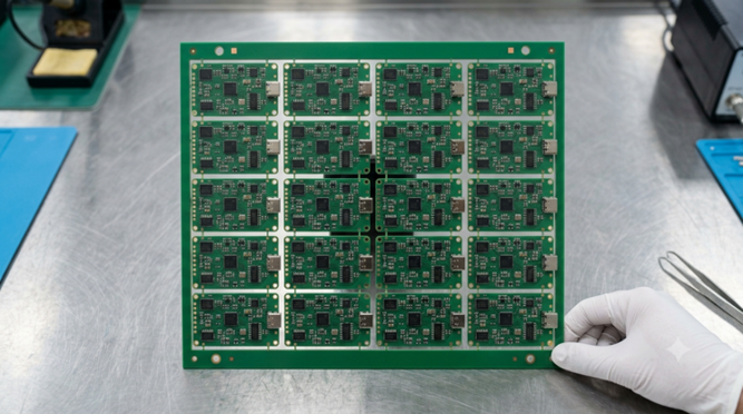
Figure 1: A fully populated production panel of PCBs before depaneling
Any space lost to rails, gaps, or unused areas is therefore shared across the boards that do fit. Once you think of the panel as the real unit of production, those spacing rules start to make more sense. This guide explains the three different things commonly called a panel, the geometry that consumes usable area, and where automated panel fitting can still fall short.
Why PCB Panel Size Can Make or Break Production Efficiency
Panel size decides how much of the material you paid for actually becomes product.
The Connection Between Panel Size, Material Utilization, and PCB Cost
A fab does not really price your board. It prices the area of panel your board consumes. Laminate, drill wear, plating chemistry, press time, and handling are all charged against the panel. Cost per board is therefore the panel cost divided by how many good boards came off it.
Utilization is the number that connects those two figures. It is the total area of your boards divided by the area of the panel that carries them. A panel running at 80% utilization spends one-fifth of its cost on scrap, so that fifth is added to every board you receive. Small changes in the board outline move that figure more than designers expect.
How Panel Dimensions Influence Manufacturing Efficiency and Yield
Every step in fabrication has a fixed cost per panel rather than per board. A drill machine loads one panel stack and runs one program, so board count never changes the setup. An electroplating line holds a fixed number of slots, and a lamination press book takes a set number of openings, whatever is inside them.
Doubling the boards on a panel, therefore, halves the share of that fixed cost each board carries. This is why a fab quoting five 100 x 100 mm (3.94 x 3.94 in) boards charges far more per board than the same fab quoting fifty of them. Bigger panels are not automatically better, since yield moves in the opposite direction. Plating current density runs higher at panel edges and corners, so copper builds up unevenly across a wide panel. Laminate also expands and contracts during pressing. That dimensional shift accumulates with distance from the tooling holes.
Standard Panel Sizes: What Designers Should Know
Three completely different things get called a panel, and mixing them up causes most of the confusion. One is bought as raw material, one belongs to the factory floor, and only the third is something you design.
Common Panel Dimensions Used in PCB Manufacturing
Copper-clad laminate arrives from the material maker as a large sheet. A typical FR-4 sheet measures 1041 x 1245 mm (41 x 49 in), with 1030 x 1230 mm (40 x 48 in) also common. That sheet is then cut down into working panels, which are the rectangles that travel through drilling, imaging, plating, and etching.
- The most common working panel is 457 x 610 mm (18 x 24 in), and its usable area is closer to 406 x 559 mm (16 x 22 in).
- Smaller shops run 305 x 457 mm (12 x 18 in), while 533 x 610 mm (21 x 24 in) suits high volume.
Your array is the third panel, and it is the only one you draw. It holds several copies of your board joined by V-scores or tabs. Rails are added for handling, and the whole thing ships to you intact so that an assembly line can process it as a single unit.
| What It Is | Typical Size | Who Decides It | What It Means for Your Design |
|---|---|---|---|
| Laminate sheet | 1041 x 1245 mm (41 x 49 in) | The material supplier | Nothing directly, but it sets the working panel sizes that follow |
| Working panel | 457 x 610 mm (18 x 24 in), usable 406 x 559 mm (16 x 22 in) | The fabricator | Your board and array must tile into this to be priced well |
| Delivery array | 70 x 70 mm up to 475 x 475 mm (2.76 to 18.7 in square) for V-cut at JLCPCB | You, or the fab on request | Rails, spacing, and the depaneling method are yours to specify |
| Single board | 3 x 3 mm (0.12 x 0.12 in) minimum, up to 670 x 600 mm (26.4 x 23.6 in) on 2 layers | You | The outline that everything above has to accommodate |
Only the bottom two rows are yours to control, which is why they are the only ones worth memorizing. JLCPCB lists the exact figures in its published board and panel dimension limits, including 663 x 593 mm (26.1 x 23.3 in) for 4 layers and 656 x 586 mm (25.8 x 23.1 in) for 6 layers and up.
Why There Is No Single Best Standard Panel Size
There is no single panel size that is always best. The most efficient choice depends on the size and aspect ratio of the boards being tiled into it.
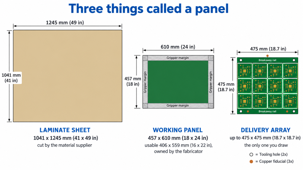
Figure 2: The three different things called a PCB panel, shown to scale
For example, A 100 x 20 mm (3.94 x 0.79 in) strip and a 60 x 60 mm (2.36 x 2.36 in) square reach their best utilization on different panels. The remainders fall differently in each case, so neither one cares what the industry average is.
Layer count further narrows the choice: a 12-layer board requires tighter registration than a 2-layer board. Fabs, therefore, run high-layer counts on smaller working panels, where lamination shift stays controllable. Equipment sets the outer boundary. V-scoring at JLCPCB works between 70 x 70 mm (2.76 x 2.76 in) and 475 x 475 mm (18.7 x 18.7 in). That is because below the minimum, the array cannot be gripped, and above the maximum, it will not pass through the scoring machine.
PCB Panelization Is More Than Fitting Boards Together
Panelization looks like a packing puzzle. The geometry around your boards is what decides whether the array can actually be built and assembled, though.
How PCB Panelization Determines Board Quantity and Layout
Board count follows from pitch rather than from board size. Pitch is the board dimension plus whatever gap the depaneling method needs. A 40 mm board separated by 2 mm routing slots, therefore occupies 42 mm of panel in that direction. Divide the usable panel length by the pitch, round down, and you have your column count.
Orientation changes the answer more often than it should. Rotating the board 90 degrees changes both divisions at once, and one of the two arrangements almost always wins. Mixing different designs on one panel is allowed and useful for prototypes. JLCPCB permits up to five designs on a single panel without an extra design charge. The ceiling is ten, and every design past the fifth is billed as a separate one.
Spacing, Rails, Tooling Holes, and Manufacturing Edges
Rails are the strips of bare laminate along the panel edge that carry the array through a machine. An SMT conveyor clamps the outer few millimeters of whatever passes along it. Any component within that band would therefore collide with the guide rails, knocking it off the wet paste.
That collision risk is why the recommended process edge at JLCPCB is 5 mm (197 mil) wide. It is enough to clamp safely, and it still leaves room for the tooling features that live there.
| Panel Feature | Recommended Size at JLCPCB | Purpose on the Line | If You Get It Wrong |
|---|---|---|---|
| Process edge (rail) | 5 mm (197 mil) wide | Gives the conveyor and clamps something safe to hold | Components near the edge get knocked off during placement |
| Tooling hole | 2 mm (79 mil) non-plated, placed asymmetrically | Locates the panel on the stencil printer and placement pins | Stencil misregistration, so paste lands off the pads |
| Fiducial mark | 1 mm (39 mil) copper dot, center 3.85 mm (152 mil) from the panel edge | Gives the placement camera a global optical reference | The machine cannot correct for panel skew or stretch |
| Board-to-board gap | 1.6 to 2.4 mm (63 to 94 mil) for routed panels, 0 mm for V-cut | Clearance for the router bit and its tolerance | Router breaks into your board outline or copper |
| Copper to routed edge | 0.2 mm (8 mil) minimum, 0.3 to 0.5 mm (12 to 20 mil) preferred | Keeps the pour clear of the cutter and its tolerance | Exposed copper burrs or a nicked ground plane |
Maximizing Panel Utilization Without Compromising Manufacturability
Squeezing the last board onto a panel is easy, and it is usually where the trouble starts. Even experienced designers make the same handful of trades. Each one has a cheap fix if you catch it before the order goes out.
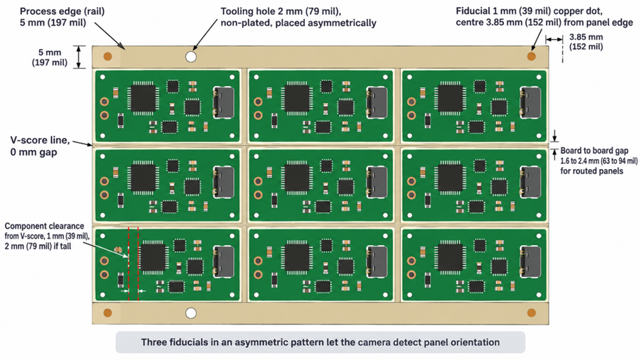
Figure 3: Panel furniture annotated on a delivery array
- Deleting the rails to gain a column removes the only surface the conveyor can grip. The assembler then either rejects the file or rebuilds your array with the rail added back. Keep the 5 mm (197 mil) edge and recover the area by shrinking your board outline instead.
- Placing tall connectors right beside a V-score line means the panel cannot be snapped without stressing the joint underneath. Components need at least 1 mm (39 mil) of clearance from a score line, and 2 mm (79 mil) if they are tall or stress sensitive.
- Rotating alternate boards to interlock two odd shapes looks efficient, but it forces mixed placement orientations on the assembly line. Keep every board in one orientation unless the utilization gain is genuinely large.
- Ignoring the fiducials because the boards look simple costs you placement accuracy on every fine-pitch part. The camera has nothing to reference, so it cannot correct for panel stretch. Three 1 mm (39 mil) fiducials in the rail take no usable area at all.
What Should You Consider When Choosing a PCB Panel Size?
Choose panel size in stages: start with the board dimensions, then check equipment limits, and finally, the depaneling method.
Board Dimensions, Layer Count, and Copper Requirements
Start with the finished board outline, including anything that extends beyond the main shape. Mounting ears, castellated edges, and connector overhangs all affect panel pitch because the router still needs enough clearance around them.
Layer count and copper weight also affect how large the panel can safely be:
- Higher layer counts need tighter registration. A 10-layer board accumulates more alignment error than a 4-layer board, so dense multilayers often use smaller arrays to keep registration within the annular-ring limit.
- Heavy copper needs longer etching. A 2 oz (70 µm) outer layer takes longer to etch than a 1-oz (35 µm) layer, and the etch rate can vary across a large panel.
- Smaller panels help reduce trace-width variation and registration error, especially on dense or heavy-copper designs.
Manufacturing Equipment and Process Limitations
Machine limits set hard boundaries that no amount of clever tiling can move. The V-scoring machine at JLCPCB accepts arrays from 70 x 70 mm (2.76 x 2.76 in) up to 475 x 475 mm (18.7 x 18.7 in). It will not score a board thinner than 0.6 mm (24 mil), because too little material would be left to hold the web together.
Scoring geometry carries its own rules, and they are worth reading before you draw an array. The published V-cut panelization standards specify a 25-degree groove, cut evenly from both faces, leaving a web of roughly one-third of the board thickness. That web is what your hands or the depaneling machine will finally break.
Routing, Depanelization, and Edge Clearance
Depaneling decides how much gap you need all along, so choose the method before you set the spacing. The three common options trade panel area against edge quality. Each one suits a different kind of board.
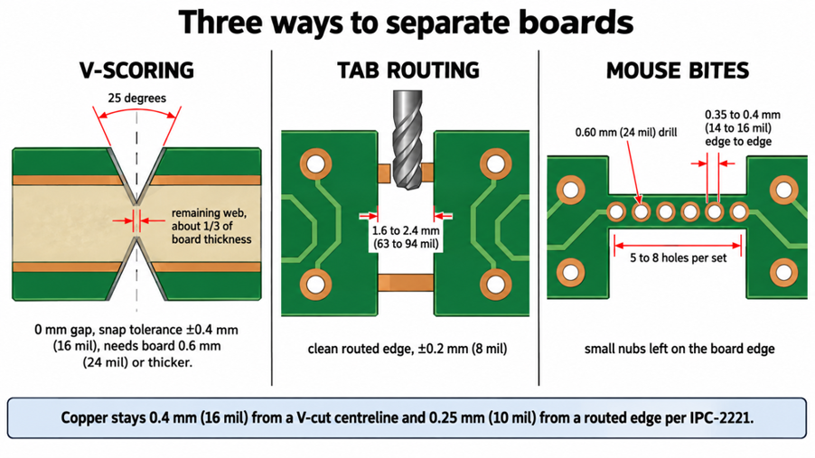
Figure 4: V-score, tab route, and mouse bite compared in cross-section
| Method | Gap Between Boards | Edge Quality and Tolerance | Best Suited To |
|---|---|---|---|
| V-scoring | 0 mm, boards butt together | Slight lip on the edge, ±0.4 mm (16 mil) after snapping | Rectangular boards in straight rows and columns |
| Tab routing | 1.6 to 2.4 mm (63 to 94 mil) | Clean routed edge, ±0.2 mm (8 mil) standard | Irregular outlines, cutouts, and boards with curved edges |
| Mouse bites | 1.6 to 2.4 mm (63 to 94 mil) | Small nubs left on the edge, needs filing if cosmetic | Small or light boards that must snap out by hand |
V-scoring wins on area every time, which is why it dominates when the boards are rectangles. Tab routing wins whenever the outline is not, and mouse bites are really tab routing with the tab perforated so a person can break it.
Mouse bite geometry controls the breaking force, so it is worth getting right. The JLCPCB mouse bite panelization guide calls for 0.60 mm (24 mil) drills in sets of five to eight holes. Edge-to-edge spacing runs 0.35 to 0.4 mm (14 to 16 mil), with 0.3 mm (12 mil) as the floor.
Using a PCB Panel Calculator for Faster Planning
A panel calculator answers one narrow question quickly. How many copies of this rectangle fit inside that rectangle? Understanding the arithmetic matters more than the tool, because the tool cannot see the constraints that actually govern your array.
Estimating How Many PCBs Fit on a Panel
The count takes under a minute by hand, and the sequence below is exactly what any calculator runs internally. Working it manually once is what teaches you which number to move when the answer disappoints you.
- Subtract the rails to get the usable area. A 200 x 150 mm (7.87 x 5.91 in) panel with 5 mm rails top and bottom gives you 200 x 140 mm.
- Add the depaneling gap to each board dimension to get the pitch. A 40 x 30 mm (1.57 x 1.18 in) V-scored board stays at 40 x 30 mm, because V-scoring adds nothing.
- Divide the usable length by the pitch in each direction and round down. That gives 200 / 40 = 5 columns and 140 / 30 = 4 rows, for a total of 20 boards.
- Repeat the division with the board rotated 90 degrees. Here,e that gives 200 / 30 = 6 columns and 140 / 40 = 3 rows, so 18 boards.
- Take the better orientation and check the utilization. Twenty boards at 1,200 mm² each, against a 30,000 mm² panel, work out to 80%.
Anything above roughly 75% utilization is healthy for a rectangular board. Falling much below 60% usually means the outline and the panel are fighting each other. The fix is normally a few millimeters off the board rather than a different panel.
Understanding the Limits of Automated Panel Calculations
An automated calculation treats your board as a plain rectangle, which is where it starts to mislead you. It has no idea that a connector overhangs the outline. It cannot see that one edge carries castellations, or that a tall electrolytic capacitor sits 1 mm from where you drew a V-score.
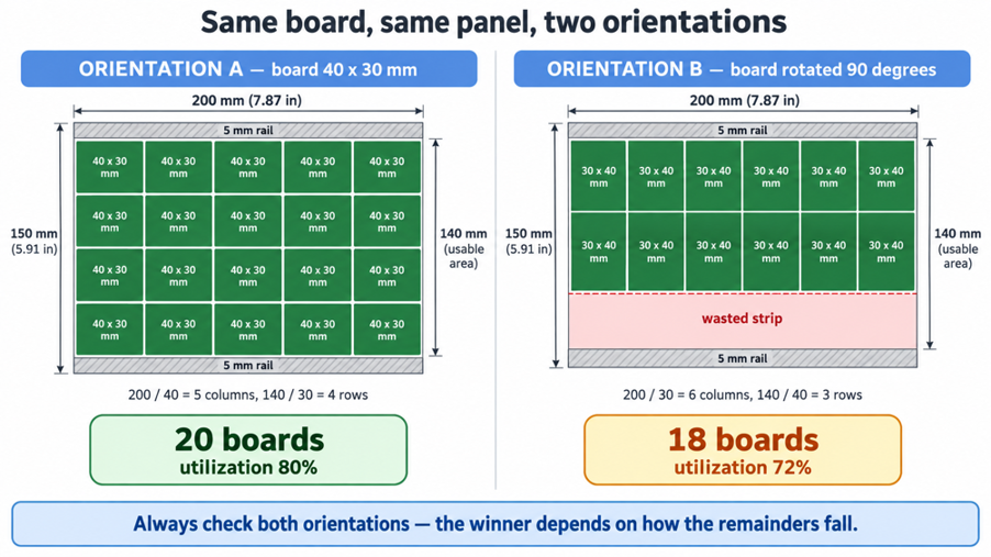
Figure 5: Boards per panel worked out in both orientations
A calculator will happily butt two boards together with a zero gap for V-scoring because, at the outline level, that is geometrically true. The parts on the top surface still need 1 mm of clearance from the score line, though, and 2 mm where they are tall or stress sensitive. Component keep-out is the constraint these tools miss most often. Orientation and assembly cost also sit outside its scope.
How Professional PCB Manufacturers Optimize Panel Production
A manufacturer sees a side of panel optimization you never do. It is arranging your array inside its own working panel, and balancing that against every other job running the same day.
Engineering Review and Panelization Optimization
Engineering review is where your Gerbers become a production panel. A CAM engineer takes your board outline and decides how many copies fit the working panel. The same engineer adds the rails, tooling holes, and fiducials the line needs, and flags spacing that a router bit cannot clear.
JLCPCB automates most of this, so you can upload your board and see the panel options before committing to anything. Choosing panel by customer or panel by JLCPCB decides who draws the array. Hand it over, and the edge rails arrive with fiducial marks and tooling holes already placed. Boards start from $2, and the panel arrangement is priced in front of you.
From Panel Design to Fabrication and Quality Inspection
Once the panel layout is fixed, everything downstream treats it as one object. Inner layers are imaged and etched as full panels, then stacked and pressed together. Lamination registration is therefore measured across the panel rather than per board, and drilling runs one program over the whole panel from the tooling holes.
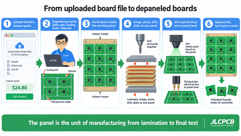
Figure 6: From uploaded board file to depaneled boards
- Inspection works at the panel level too, for the same reason. Automated optical inspection scans the panel and compares each board against the design data.
- Depaneling comes last, deliberately. Separating the boards earlier would mean handling dozens of small pieces through the finishing steps.
The panel is the unit of manufacturing from lamination to the final test. Your boards only become individual objects in the last few minutes of the process.
FAQ About PCB Panel Size
Q: What is the maximum PCB panel size I can order?
For V-cut arrays at JLCPCB, the limit is 475 x 475 mm (18.7 x 18.7 in), with a minimum of 70 x 70 mm (2.76 x 2.76 in). Routed and mouse-bite panels follow the single-board maximums instead, which reach 670 x 600 mm (26.4 x 23.6 in) on 2-layer FR-4 and 656 x 586 mm (25.8 x 23.1 in) from 6 layers up.
Q: Should I panelize my board myself or let the manufacturer do it?
Let the manufacturer do it unless you have a specific reason not to, because the fab knows its own working panel size and will arrange your board to suit it. Panelize yourself when you need a particular depaneling method, a fixed board orientation for assembly, or several different designs deliberately grouped on one array.
Q: Does a bigger panel always make my boards cheaper?
Not always, since yield falls as panels grow. Plating uniformity, etch rate, and layer registration all vary more across a large panel. A high layer count or heavy copper design can therefore lose more to scrap than it saves on fixed cost, which is why fabs cap panel size by layer count.
Q: How much panel area do the rails and spacing actually consume?
More than most people expect from small arrays. Two 5 mm (197 mil) rails on a 200 mm (7.87 in) panel take 5% of the length straight away. Routing gaps of 2 mm (79 mil) between 40 mm boards add another 5% in that direction, so combined overhead often runs 10 to 20% of the panel.
Q: Can I mix different board designs on one panel?
Yes, and it is a common way to prototype a product family on one order. JLCPCB allows up to five designs on a single panel without an extra design charge, and up to ten in total. Each design past the fifth is billed as a separate one, and all of them must share the same stackup, thickness, and surface finish.
Conclusion
PCB panel size stops being an abstract manufacturing detail once you see what a factory actually makes. It makes panels, not boards. Your price per board is the panel price divided by the good boards that came off it, so every millimeter of rail, gap, and unused corner is already inside your quote.
Boards keep shrinking while assembly lines keep demanding the same 5 mm of edge to hold onto. The fraction of a panel spent on handling, therefore, rises as products get smaller. Check both orientations, respect the keep-outs, and let engineering review tell you what the last 2 mm is worth. JLCPCB's instant quoting and automatic panelization make it a cheap check on every revision.

Keep Learning
Design for Manufacturing and Assembly: A Complete DFMA for PCB Design Guide
Key Takeaways DFMA covers both PCB fabrication and assembly: DFM addresses bare-board fabrication, while DFA addresses component assembly and related process constraints. The biggest decisions happen early: Package choice, layer count, and board outline are usually set well before Gerber export and become expensive to change later. Passing DRC does not guarantee a good footprint: Design rules can verify clearances and copper geometry, but they cannot confirm that a footprint matches the component data......
Get More From Every PCB Panel: Choosing the Right Panel Size
Key Takeaways Panel Drives Cost: Fabs price the whole panel, so maximizing utilization lowers per-board cost. 3 Panel Types: Distinguish raw sheets, fab working panels, and your delivery array. Keep Clearances: Reserve 5 mm process rails and 1–2 mm spacing around V-scores. Match Depaneling Method: Use V-cut (0 mm gap) for rectangles, tab routing for complex shapes. Test Both Orientations: Rotate boards 90° to find the best fit before ordering. PCB panel size is the one number on your order that you ne......
Free DFM Tool: Enhancing PCB Design Efficiency
Design for Manufacturability (DFM) guarantees that the design is best suited for manufacturing and assembly, it is a key process in printed circuit board (PCB) design. Using a Free DFM Tool will improve accuracy and efficiency, by greatly streamlining this process. The advantages of Free DFM Tools, their place in PCB design, and how they could affect your projects are discussed in this article. We will also discuss some typical problems and fixes related to using these tools, highlighting their applic......
Understanding the Importance of DFM Analysis in PCB Design
Design for Manufacturing (DFM) analysis helps you on whether a printed circuit board (PCB) is fit for manufacturing, assembly, and sales. Early in the planning process, it looks for and fixes any possible problems arising throughout production. This will increase manufacturing efficiency and help to save expenses. DFM analysis is quite vital in the complex world of electronics, where even little design errors can create delays costing a lot of money. This article discusses the different types of DFM i......
Thermal Vias in PCB Design for Heat Management
Thermal vias are specialized vias designed to transfer heat from one layer of a PCB to another. These vias are placed near heat-generating components to create a thermal pathway, helping to dissipate heat and reduce the risk of overheating. They are often used with heat sinks, thermal pads, or copper planes to enhance their effectiveness. They are simply plated through holes (PTHs) that are located under a surface-mounted heat source component in a printed circuit board (PCB) that allow heat transfer.......
The Ultimate Guide to PCB Panelization: Tools and Techniques
Printed circuit boards (PCBs) are the backbone of modern electronics. One critical aspect of PCB manufacturing is panelization — the process of arranging multiple PCBs onto a single larger panel for efficient manufacturing and assembly. This technique allows multiple boards to be processed simultaneously, significantly reducing costs and improving production efficiency. In this article, we will provide a comprehensive guide to PCB panelization, covering the tools and techniques required for successful......