Design for Manufacturing and Assembly: A Complete DFMA for PCB Design Guide
15 min
- What Is DFMA (Design for Manufacturing and Assembly)?
- Why DFMA Starts at Component Selection, Not Gerber Export
- DFM for PCBs: Designing the Bare Board for Reliable Fabrication
- DFA for PCBs: Designing the Board for Efficient Assembly
- PCB Panelization, Stencil Design, and Reflow
- DFMA for PCB Assembly Data: BOM and Pick-and-Place Files
- Conclusion
- FAQs about DFMA (Design for manufacturing and assembly)

Key Takeaways
- DFMA covers both PCB fabrication and assembly: DFM addresses bare-board fabrication, while DFA addresses component assembly and related process constraints.
- The biggest decisions happen early: Package choice, layer count, and board outline are usually set well before Gerber export and become expensive to change later.
- Passing DRC does not guarantee a good footprint: Design rules can verify clearances and copper geometry, but they cannot confirm that a footprint matches the component datasheet.
- Assembly files matter as much as the PCB layout: Incorrect BOM data, component rotation, or pick-and-place coordinates can prevent assembly even when the board itself passes all layout checks.
- PCB cost is driven by process complexity: A small board can still be expensive if it requires extra layers, special drilling, tight tolerances, or additional manufacturing steps.
DFMA (Design for Manufacturing and Assembly) is the bridge between a PCB that functions electrically and one that can be consistently manufactured and assembled.
A board can pass every electrical check and still cause problems in production. A footprint may not match the actual component, a connector may sit too close to the board edge, or the panel may leave no room for handling. Any of these issues can delay or stop assembly.
This guide looks at DFMA specifically for PCB design: which decisions create manufacturing constraints, when those decisions should be made, and when they become expensive to change.
In this guide, you will learn:
- How DFM, DFA, and DFMA divide the work of getting a board built
- Which layout decisions cost the most to reverse
- How package choice, spacing, and panelization drive assembly yield
- Why the BOM and the pick-and-place file are DFMA documents too
- Which design choices move the PCB cost the most
The table below shows what to check at each design stage and which decisions become difficult or costly to change once you move to the next stage.
| Design Stage | What to Check Here | What Is Impractical to Change After This |
|---|---|---|
| Schematic and BOM draft | Package availability, inspection method, and through-hole count | The package family and the inspection step commit you to |
| Stackup and outline | Layer count, via strategy, board dimensions, mounting | Layer count, because impedance and routing both depend on it |
| Placement | Spacing, orientation consistency, rework access, board face | Which face each part sits on, and the second reflow pass |
| Routing and copper | Process margin, copper balance, copper-to-edge clearance | Trace geometry on impedance-controlled nets |
| Pre-release | Footprints against datasheets, silkscreen, paste layer | Footprint errors, once parts are ordered against them |
| File preparation | Panel format, BOM, and pick-and-place columns, rotations | Panel format, once the order enters production |
What Is DFMA (Design for Manufacturing and Assembly)?
Design for Manufacturing and Assembly (DFMA) looks at two sides of the same problem: can the bare PCB be fabricated within the manufacturer's normal process limits, and can the finished board be assembled efficiently by machine?
DFM (Design for Manufacturability) covers the first question, while DFA (Design for Assembly) covers the second.
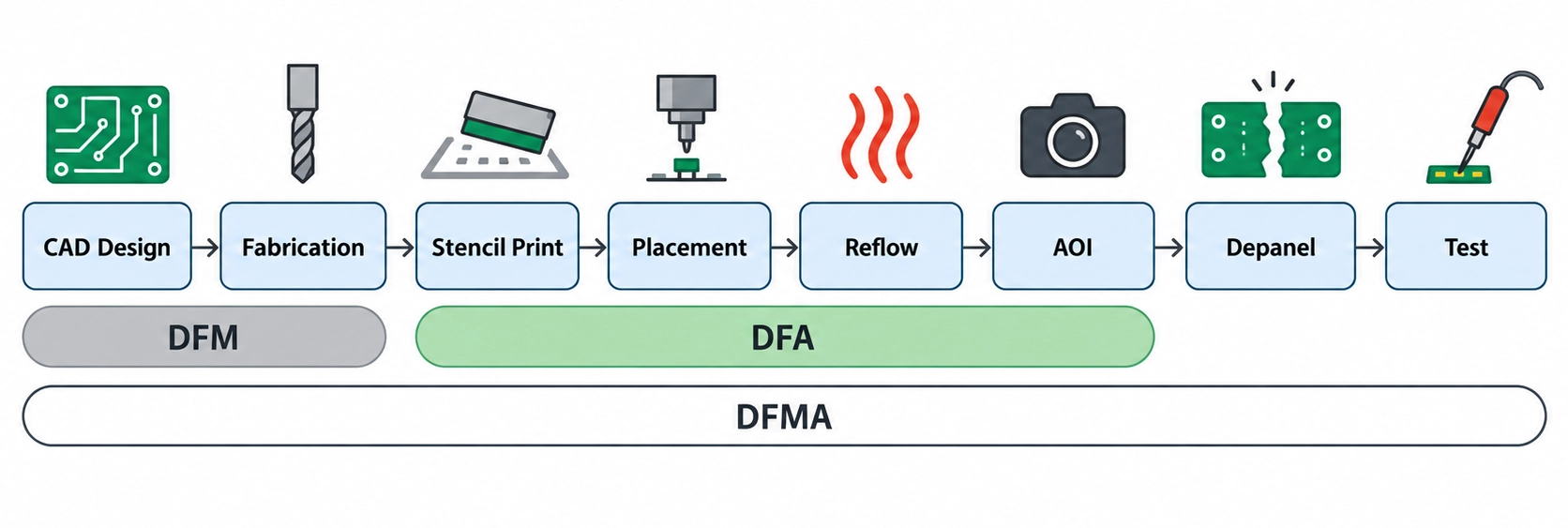
Figure: The PCB production chain from CAD to test
The method was formalized by Geoffrey Boothroyd and Peter Dewhurst in the 1980s for mechanical products, but the same principles apply naturally to PCB design.
Their original work used the term "Design for Manufacture and Assembly"; today, "design for manufacturing and assembly" is more commonly used to describe the same approach.
Problems usually appear when fabrication and assembly are treated as separate concerns. The PCB fabricator focuses on copper, holes, spacing, and stackup, while the assembly line focuses on footprints, component access, orientation, and placement.
| Discipline | The Question It Asks | What It Governs on a PCB | Typical Consequence If Ignored |
|---|---|---|---|
DFM (Design for Manufacturability) | Can this bare board be etched, drilled, plated, and routed? | Copper geometry, drill sizes, layer count, outline, and material | Yield loss at the fab, scrapped panels, a requote |
DFA (Design for Assembly) | Can a machine place, solder, and inspect every part? | Packages, spacing, footprints, polarity marks, panel format | Hand placement, rework, tombstoned, or bridged joints |
DFMA (Design for Manufacturing and Assembly) | Can this design be built end-to-end, at the intended volume? | The order of decisions and the trade-offs between the two halves | A board that clears each check separately and still stalls |
Table: Comparison table of DFM, DFA, and DFMA
Why DFMA Starts at Component Selection, Not Gerber Export
Before Gerber export, three key design choices are already fixed, and they shape most of what the manufacturer can do:
- The package family determines the soldering and inspection steps the board requires.
- Layer count decides the stackup, the impedance targets, and much of the panel cost.
- Board outline, decides panelization, mounting, and mechanical fit.
A DFM check at export can therefore only report what has already become expensive to change.
For example, selecting a BGA shows how much a single package commits. It sets the minimum layer count needed to escape-route out of the ball field, and it commits the board to X-ray inspection, because a top-down camera cannot see joints under the package body.
- Changing that package during schematic capture costs an afternoon of library work.
- Changing it after layout means rerouting, rechecking impedance, and reordering parts.
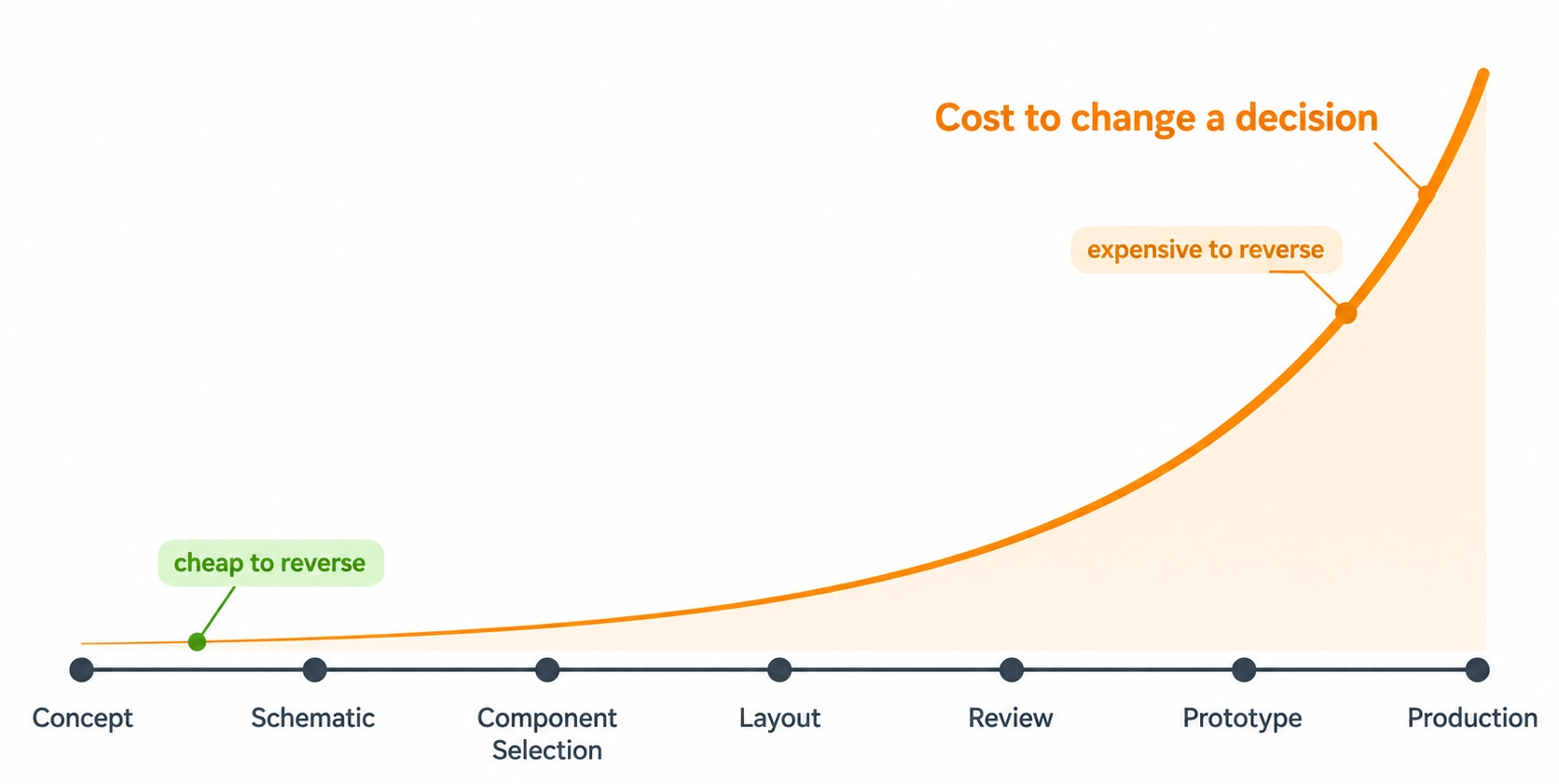
Figure: The PCB design timeline from concept to production with a cost-of-change curve
A useful DFMA review should happen while the BOM is still taking shape. Wait until Gerber export, and you are mostly checking decisions that are already difficult and expensive to change. Part selection is also easier when manufacturing data is available early.
DFM for PCBs: Designing the Bare Board for Reliable Fabrication
DFM (Design for Manufacturability) asks whether the bare board can be etched, drilled, plated, and routed inside the fab's normal process window. The question is not whether a single board is possible, but whether the result repeats across the entire panel.
Designing With Process Margin, Not at the Minimum
A published manufacturing minimum is a process limit, not an ideal design target. Designing right at that limit leaves little room for normal variation in etching, layer registration, drilling, and plating.
Moving one step away from the minimum usually costs very little board area, but it gives the fabrication process much more margin. The PCB manufacturer’s capability table tells you what is possible; the PCB design rules should tell you what is practical.
That margin usually disappears in the same few areas:
- Trace width and spacing set at the minimum leave almost no room for normal etching variation across the panel.
- Drill-to-copper spacing at the limit is risky because both drill position and layer registration can shift slightly during fabrication.
- The fab may clip Silkscreen placed over pads or vias, or, if left in place, interfere with soldering.
- Very thin solder mask slivers between fine-pitch pads may not reliably survive mask development.
- A board outline with no tolerance allowance gives the routing process no room for normal mechanical variation.
PCB Fabrication Cost Drivers: Vias, Copper, and Layer Count
Several layout choices directly affect how difficult and expensive a PCB is to manufacture:
1. Via and drill choices
Every drill diameter requires a separate tool, while very small drill bits run more slowly and wear or break more easily. The finished hole must also remain within its copper pad despite normal drilling and registration variations, which is why the annular ring matters.
Blind and buried vias add even more cost because they can require extra drilling, plating, and lamination cycles.
2. Copper near the board edge
Copper placed too close to the finished outline can be damaged during routing or depaneling. The router bit may expose copper, create burrs, or damage the laminate, so traces and copper pours are normally pulled back from the edge.
3. Copper balance
Uneven copper density across the stackup can affect resin flow during lamination and increase the risk of bow or twist. Non-functional copper fill is often added to keep copper distribution more balanced between layers.
4. Layer count
Each additional layer pair adds more imaging, etching, lamination, registration, and inspection work. Layer count is also difficult to change late in the design. Dropping from six layers to four can shift reference planes, alter impedance, reduce routing space, and necessitate a major reroute.
These choices may look like simple layout details, but they directly influence the fabrication process, yield, and final PCB cost.
DFA for PCBs: Designing the Board for Efficient Assembly
DFA (Design for Assembly) asks whether a machine can place, solder, and inspect every part without human intervention, since each intervention is slower than the step it replaces.
Choosing Assembly-Friendly Packages
Package choice sets how the board is built, not only how much room it occupies. Through-hole parts require a separate soldering step after reflow, so even a few connectors can add an extra assembly process.
For example, a 0201 resistor is only 0.6 × 0.3 mm, compared with 1.0 × 0.5 mm for a 0402—that smaller size demands finer solder paste and more precise placement. Unless board space is extremely tight, the larger 0402 package is generally easier and more forgiving to assemble.
Component Spacing for Placement, Inspection, and Rework
PCB spacing serves four different purposes, so a single clearance value rarely works for every situation:
- A placement nozzle needs room to descend without striking a neighboring part.
- A rework iron or hot-air tip requires a wider approach than the nozzle.
- An AOI camera needs an unshadowed view of the joint it is judging.
- Printed paste needs somewhere to go if the deposit slumps during reflow.
Tall parts cast the longest shadows, so a connector beside a fine-pitch device can hide joints the camera needs to see. Check the minimum spacing guidance for SMD components before placement is frozen.
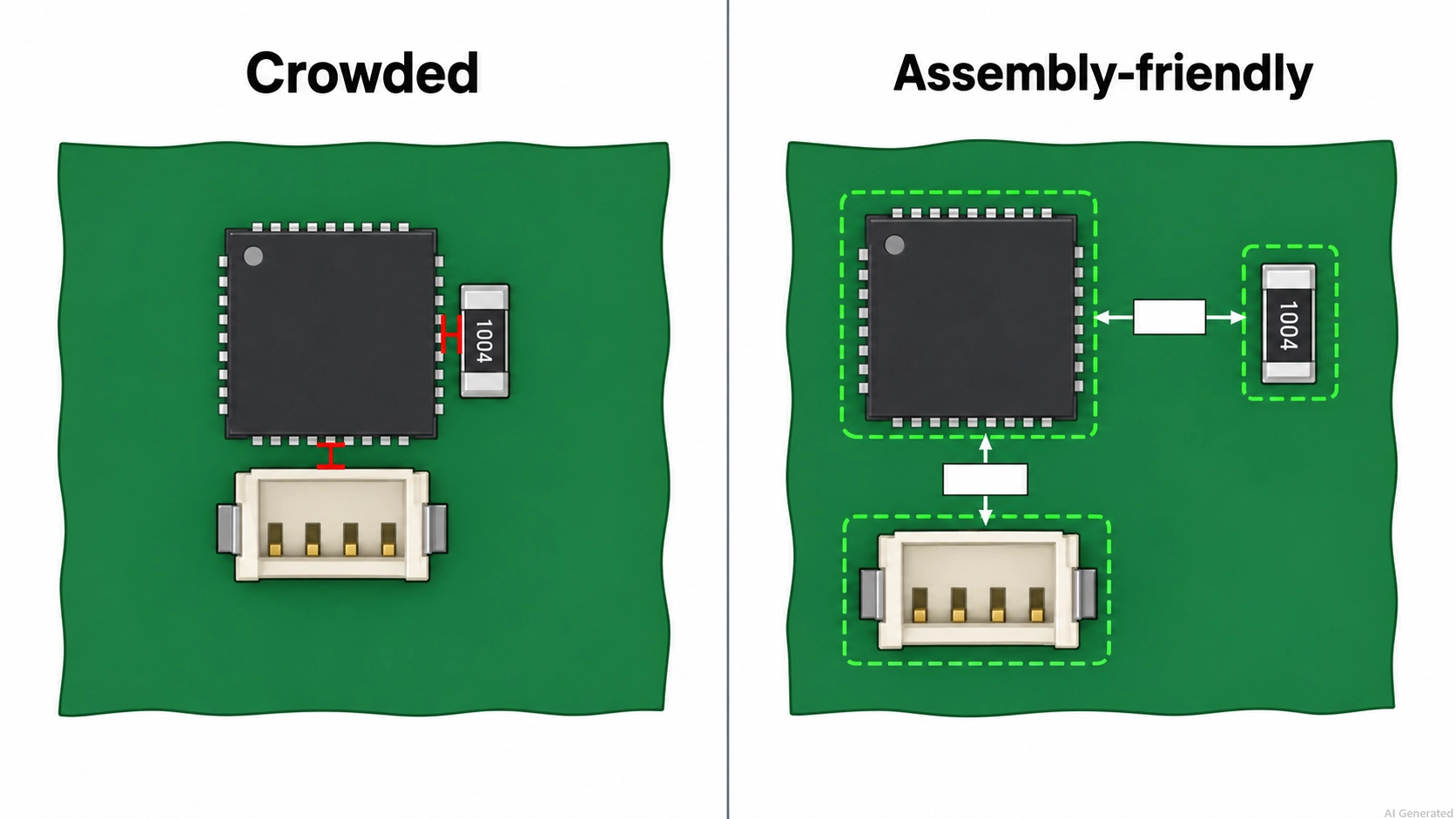
Figure: Crowded SMD placement compared with assembly-friendly component spacing
Verifying PCB Footprints Against Component Datasheets
A footprint can pass DRC and still be unbuildable, because a design rule check compares copper against copper and never opens the datasheet. It cannot report that a pad is too short for the lead.
IPC-7351B defines how land patterns are derived, though library footprints follow it to varying degrees. Comparing a new footprint against the manufacturer's recommended pattern takes minutes. Most of it comes down to three things:
- Pad length and width, which decide whether the lead has enough area to form a fillet.
- Thermal pad dimensions, which decide how the package sits and how heat leaves it.
- Pin 1 location and the silkscreen marker, which decide how the part is oriented.
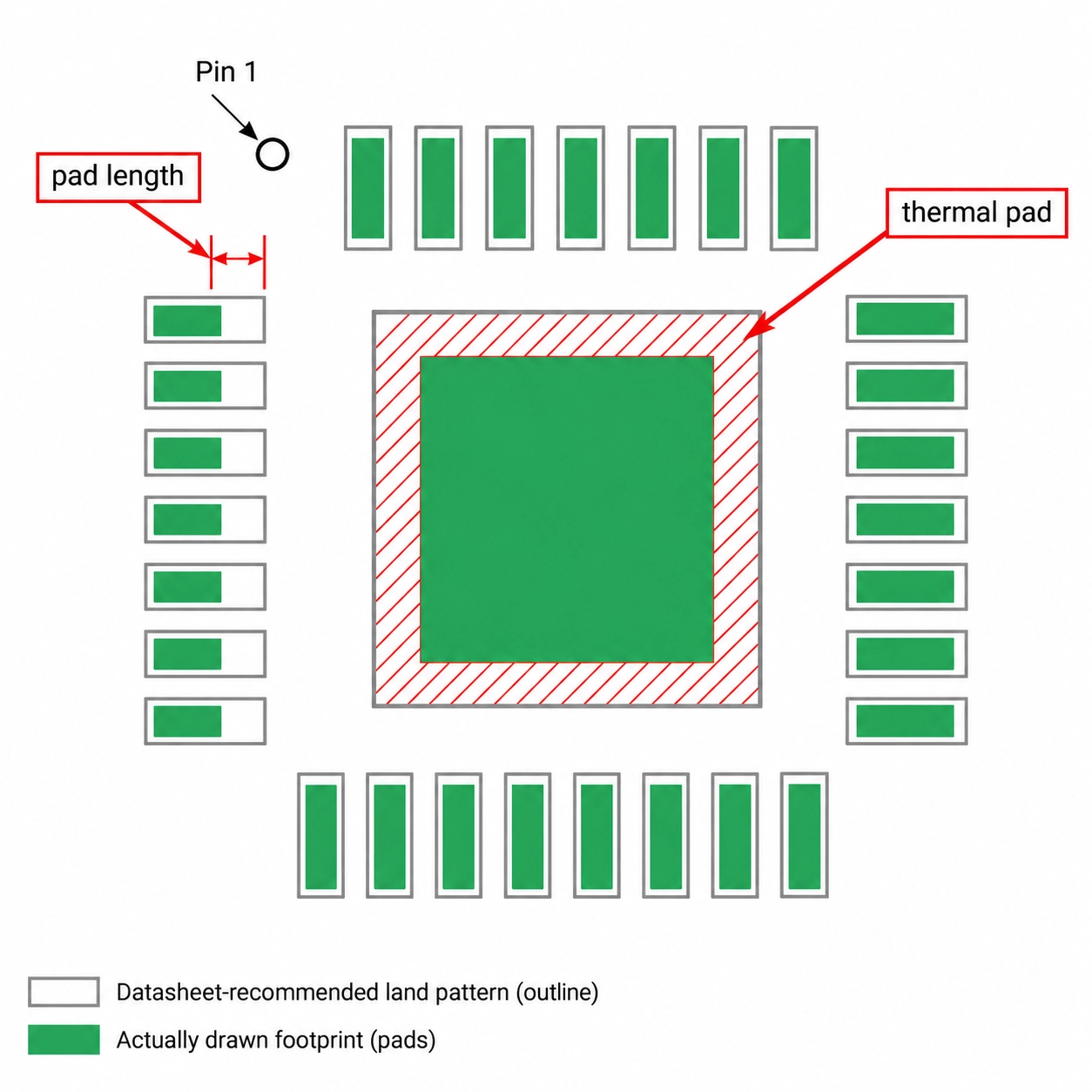
Figure: A QFN footprint overlaid on its datasheet land pattern
Design for Inspection, Test, and Rework
Inspection, testing, and rework all depend on physical access. A solder joint that cannot be seen is harder to inspect, while a component surrounded by tall parts is harder to replace. These constraints should be considered during placement, not after the layout is finished.
1. Inspection access
AOI uses reflected light to inspect only joints visible to the camera. Keep exposed joints clear of tall neighboring components that may block the view. Solder joints beneath BGA, QFN, and other leadless packages are hidden and typically require X-ray inspection.
2. Test and programming points
Dedicated test pads usually take less space than programming headers and avoid adding another connector to the BOM. Exposed pads can be contacted with pogo pins during production testing or programming.
3. Rework clearance
Components that may need replacement should have enough space around them for an iron, hot-air nozzle, or rework tool. A fine-pitch IC surrounded by tall capacitors or connectors can be difficult to remove without shielding or disturbing nearby parts.
4. Package choice
Where density allows, consider a leaded alternative to a leadless package. Visible leads simplify optical inspection and generally make probing and rework easier.
A layout is easier to manufacture when inspection points, test access, and rework space are designed in from the beginning rather than added after placement is complete.

When the design is ready, upload your files for an instant quote.
JLCPCB checks your fabrication and assembly requirements against the submitted design files, so you can review the manufacturing cost before placing your order.
PCB Panelization, Stencil Design, and Reflow
For panelized SMT production, the panel becomes the handling unit, so panel design affects how the boards are printed, placed, inspected, and separated.
Designing the Panel, Not Just the Board
Conveyors, stencil printers, and placement machines grip a panel along its edges, so a board carrying parts near its outline cannot be handled on its own. A production panel, therefore, needs four features that an individual PCB does not:
- Breakaway rails along the conveyor edges, giving the machines something to hold.
- Tooling holes in those rails, which locate the panel in the stencil printer.
- Global fiducials, which let the placement head correct for panel skew.
- A separation method, either V-cut scoring or tab routing with mouse bites.
V-cut suits have rectangular outlines, while tab routing handles irregular ones at the cost of a rougher edge. Panelization tools and techniques cover the trade-offs, and the panel guidance for assembly orders sets out what the line expects.
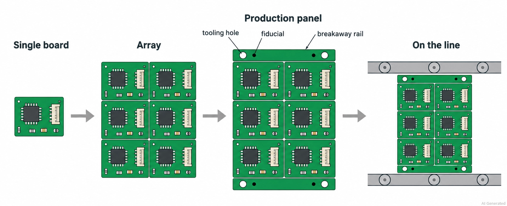
Figure: A board becoming a production panel with breakaway rails, tooling holes, and fiducials
Stencil Apertures, Thermal Pads, and Reflow Balance
Every reflowed solder joint starts with a printed paste deposit, and the stencil aperture controls how much paste is applied. Since solder paste is a mix of metal powder and flux, its volume drops during reflow as the flux evaporates.
That makes aperture design important: too little paste can starve the joint, while too much can cause bridging.
Large thermal pads under QFN and DFN packages are where this matters most. A single solid aperture floods the pad, floats the package on molten solder, and can trap flux as voids. A windowpane aperture pattern gives that flux an escape route.
A pad tied directly into a large copper pour also heats more slowly than the opposite pad, so one end of a chip component can wet before the other and pull the part upright. Thermal relief spokes even out that imbalance.
DFMA for PCB Assembly Data: BOM and Pick-and-Place Files
An assembly machine is driven by data files, not by a layout: the Gerbers build the board, while the BOM and the pick-and-place file decide what lands on it.
The BOM requirements for assembly cover designator, quantity, and part number. The pick-and-place file requirements cover position, layer, and rotation.
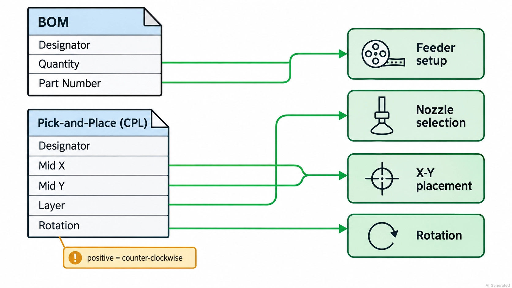
Figure: BOM and pick-and-place file columns mapped to the SMT machine actions
There may be some data errors that account for most assembly holds, and none are visible in a layout viewer:
- Wrong rotation: A pick-and-place file states rotation in degrees, measured counter-clockwise from the part's zero-degree orientation. EDA libraries do not all share that reference, and polarized parts suffer most.
- Wrong centroid: Mid X and Mid Y must sit at the true center of the part body. A centroid inherited from an odd-shaped pad places the part offset from its own footprint.
- Wrong side: The Layer column states top or bottom, so a part assigned to the wrong face will not reach the side the design intends.
- Designators that disagree: If the BOM calls a part C12 while the placement file calls it C102, the rows cannot be matched, and the job stops for clarification.
Conclusion
DFMA is less about completing a checklist than making manufacturing and assembly decisions while they are still easy to change.
Reviewing package choices, stackup, placement, footprints, and production data early in the design process makes changes easier and helps avoid costly rework later.
An online PCB DFM tool can help identify manufacturing and assembly issues before the board goes into production.
The goal is simple: design a PCB that is not only electrically correct, but also practical to fabricate, assemble, inspect, and test consistently.
FAQs about DFMA (Design for manufacturing and assembly)
Q: What Does DFMA Stand For?
DFMA stands for design for manufacturing and assembly. DFM asks whether the bare board can be fabricated reliably, while DFA asks whether the populated board can be built by machine. DFMA applies both questions to one design.
Q: What Is the Difference Between DFM and DFMA?
DFM is one-half of DFMA. It covers only the fabrication of the bare board: copper geometry, drilling, plating, and layer count. DFMA adds the assembly half, so both sets of constraints are weighed in a single decision.
Q: Why Does DFMA Matter in PCB Design?
A PCB can pass every electrical check and still be slow or impractical to build. DFMA surfaces those problems while they remain cheap to fix, because decisions about package and layer counts become costly to reverse once the layout is complete.
Q: When Should a DFMA Review Happen?
A DFMA review works best in stages rather than all at once. Check package and layer choices during schematic capture, spacing and orientation at placement, then footprints, panel format, and data files before release.
Q: Does DFMA Reduce PCB Manufacturing Cost?
It generally reduces cost by removing production steps rather than by shrinking the board. Through-hole vias instead of buried ones, or 0402 passives instead of 0201, each removes a process demand.
Q: Is DFMA Only for High-Volume Production?
No. Prototypes benefit too, because the errors that lower yield at volume also stall a five-board order. A footprint mismatch or a missing panel rail holds a small build as effectively as a large one.
Keep Learning
Design for Manufacturing and Assembly: A Complete DFMA for PCB Design Guide
Key Takeaways DFMA covers both PCB fabrication and assembly: DFM addresses bare-board fabrication, while DFA addresses component assembly and related process constraints. The biggest decisions happen early: Package choice, layer count, and board outline are usually set well before Gerber export and become expensive to change later. Passing DRC does not guarantee a good footprint: Design rules can verify clearances and copper geometry, but they cannot confirm that a footprint matches the component data......
Get More From Every PCB Panel: Choosing the Right Panel Size
Key Takeaways Panel Drives Cost: Fabs price the whole panel, so maximizing utilization lowers per-board cost. 3 Panel Types: Distinguish raw sheets, fab working panels, and your delivery array. Keep Clearances: Reserve 5 mm process rails and 1–2 mm spacing around V-scores. Match Depaneling Method: Use V-cut (0 mm gap) for rectangles, tab routing for complex shapes. Test Both Orientations: Rotate boards 90° to find the best fit before ordering. PCB panel size is the one number on your order that you ne......
Free DFM Tool: Enhancing PCB Design Efficiency
Design for Manufacturability (DFM) guarantees that the design is best suited for manufacturing and assembly, it is a key process in printed circuit board (PCB) design. Using a Free DFM Tool will improve accuracy and efficiency, by greatly streamlining this process. The advantages of Free DFM Tools, their place in PCB design, and how they could affect your projects are discussed in this article. We will also discuss some typical problems and fixes related to using these tools, highlighting their applic......
Understanding the Importance of DFM Analysis in PCB Design
Design for Manufacturing (DFM) analysis helps you on whether a printed circuit board (PCB) is fit for manufacturing, assembly, and sales. Early in the planning process, it looks for and fixes any possible problems arising throughout production. This will increase manufacturing efficiency and help to save expenses. DFM analysis is quite vital in the complex world of electronics, where even little design errors can create delays costing a lot of money. This article discusses the different types of DFM i......
Thermal Vias in PCB Design for Heat Management
Thermal vias are specialized vias designed to transfer heat from one layer of a PCB to another. These vias are placed near heat-generating components to create a thermal pathway, helping to dissipate heat and reduce the risk of overheating. They are often used with heat sinks, thermal pads, or copper planes to enhance their effectiveness. They are simply plated through holes (PTHs) that are located under a surface-mounted heat source component in a printed circuit board (PCB) that allow heat transfer.......
The Ultimate Guide to PCB Panelization: Tools and Techniques
Printed circuit boards (PCBs) are the backbone of modern electronics. One critical aspect of PCB manufacturing is panelization — the process of arranging multiple PCBs onto a single larger panel for efficient manufacturing and assembly. This technique allows multiple boards to be processed simultaneously, significantly reducing costs and improving production efficiency. In this article, we will provide a comprehensive guide to PCB panelization, covering the tools and techniques required for successful......